Transcription
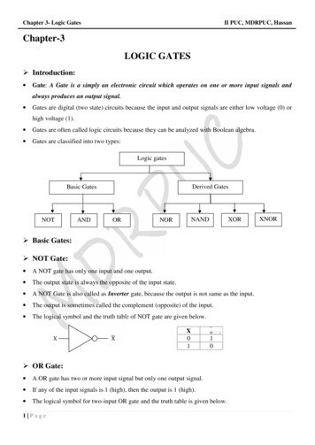
Chapter 3- Logic GatesII PUC, MDRPUC, HassanChapter-3LOGIC GATES Introduction: Gate: A Gate is a simply an electronic circuit which operates on one or more input signals andalways produces an output signal. Gates are digital (two state) circuits because the input and output signals are either low voltage (0) orhigh voltage (1). Gates are often called logic circuits because they can be analyzed with Boolean algebra. Gates are classified into two types:Logic gatesDerived GatesBasic GatesNOTANDORNANDNORXOR Basic Gates: NOT Gate: A NOT gate has only one input and one output. The output state is always the opposite of the input state. A NOT Gate is also called as Inverter gate, because the output is not same as the input. The output is sometimes called the complement (opposite) of the input. The logical symbol and the truth table of NOT gate are given below.XXX0110 OR Gate: A OR gate has two or more input signal but only one output signal. If any of the input signals is 1 (high), then the output is 1 (high). The logical symbol for two-input OR gate and the truth table is given below.1 PageXNOR
Chapter 3- Logic GatesII PUC, MDRPUC, HassanXF X YY AND Gate:X0011Y0101F X Y0111 A AND gate has two or more input signal but only one output signal. When all the input signals are 1 (high), the output is 1 (high), otherwise the output is 0. The logical symbol for two-input AND gate and the truth table is given below.XF X .YYX0011Y0101F X.Y0001 NOR Gate: A NOR gate has two or more input signal but only one output signal. The NOR gate is a complemented of OR gate. The output of NOR gate will be 1 only when all inputs are 0 and output will be 0 if any inputrepresents a 1. NOR is short form of NOT-OR. The symbol is used to represent a NOR operation. So X Y can be written as X NOR Y or X Y. The logical structure shows an OR gate and NOT gate. For input X and Y, the output of the OR gatewill be X Y which is fed as input to the NOT gate. So the output of NOR gate is given by X Ywhich is equal to X . YXF X YY F X YThe logical symbol for two-input NOR gate and the truth table is given below.XYX00112 PageY0101F 1000 F X YX00001111Y00110011Z01010101F 10000000
Chapter 3- Logic GatesII PUC, MDRPUC, Hassan NAND Gate: A NAND gate has two or more input signal but only one output signal. The NAND gate is a complemented of AND gate. The output of NAND gate will be 0 only when all inputs are 1 and output will be 0 if any inputrepresents a 0. NAND is short form of NOT-AND. The symbol is used to represent a NOR operation. So X . Y can be written as X NAND Y or X Y. The logical structure shows an AND gate and NOT gate. For input X and Y, the output of the ORgate will be X .Y which is fed as input to the NOT gate. So the output of NAND gate is given byX . Y which is equal to X YXF X .YF X.YY The logical symbol for two-input NAND gate and the truth table is given below.XYX0011Y0101F 1110. XOR (Exclusive-OR) Gate:F X .YX00001111Y00110011Z01010101F 11111110. . An exclusive-OR has two or more input signal but only one output signal. Exclusive-OR gate is different form of OR gate. Exclusive-OR gate produces output 1 for only those input combinations that have odd number of 1’s. The output is 0 if there are even number of 1’s in the input. The output is 1 if there are odd number of 1’s in the input. In Boolean algebra, ϴ sign stands for XOR operation. Thus X XOR Y can be written as XϴY If the output is given by:F XϴY3 Page
Chapter 3- Logic Gates II PUC, MDRPUC, HassanF XY XYThe XOR gate has a symbol similar to OR gate, except the additional curved line of the input side.XY F XϴY XY XYThe following truth table illustrates XOR operation for 2 and 3 inputs.NumberOf 1’sEVENODDODDEVENInputX0011Y0101OutputF XϴY0110Numberof 1’sXYZF 10101010101101001 XNOR (Exclusive-NOR) Gate: The XNOR gate is complement of XOR gate. The output of XNOR is 1 only when the logic values of both X and Y is same i.e. either both areequal to 1 or both are 0. Its output is 0 when its inputs are different. In Boolean algebra, ʘ sign stands for XNOR operation. Thus X XNOR Y can be written as X ʘ Y If the output is given by:F XʘY F XY XYThe XNOR gate has a symbol similar to NOR gate, except the additional curved line of the input side.XY F X ʘ Y XY X YThe following truth table illustrates XOR operation for 2 and 3 inputs.NumberOf 1’sEVENODDODDEVEN4 PageInputX0011Y0101OutputF X ʘY1001Numberof 1’sXYZF XʘY ʘ 10110010110
Chapter 3- Logic GatesII PUC, MDRPUC, Hassan Universal Gate (NAND & NOR): Universal gate is a gate using which all the basic gates can be designed. NAND and NOR gate re called as Universal Gates, because all the Boolean functions can also beimplemented using these two gates. NAND and NOR gates are more popular as these are less expensive and easier to design. Realization of all basic gates using NAND gate: NAND to NOT: In the figure we have two input NAND gate whose inputs are purposely connected together so thatthe same input is applied to both.F X .X XX From the diagram X NAND X NAND to AND: X .X X X// DeMorgan’s 2nd Theorem XX X X Inverted Input NOT gate In the figure we have two NAND gates connected so that the AND operations is performed. NAND gate 2 is used as a NOT gate.F1 X . YXY From the diagram X NAND YF2F2 F1 X .YF1 . F1F1 F1X. YX.YAND gateF2 X. Y X.Y// DeMorgan’s 2nd TheoremX X X NAND to OR: The OR operation can be implemented using NAND gates connected as shown in figure. NAND gate 1 and NAND gate 2 are used as NOT to invert the inputs.XY5 PageF1 XF2 YF3 X . Y X Y
Chapter 3- Logic Gates II PUC, MDRPUC, HassanFrom the diagram X NAND YF1F2F3F3 X .X X X XY .Y Y Y YF1 . F2F1 F2// DeMorgan’s 2nd TheoremX YX X and Y YX YOR gate Realization of all basic gates using NOR gate: NOR to NOT: Figure shows that NOR gate with its inputs connected together behaves as a NOT gate.F X X XX From the diagram X NOR X NOR to AND: X XX .X// DeMorgan’s 1st TheoremXX .X XInverted Input NOT gateThe AND operation can be implemented with NOR gate as shown in figure. Here NOR gate 1 andNOR gate 2 are used as NOT gate to invert inputs.F1 XXF2 YY From the diagram X NOR YF1 F2 F3 F3X X X . X XY Y Y . Y YF1 F2 F1 . F2 X .YX.Y AND gate 6 PageF3 X Y X.Y// DeMorgan’s 1st TheoremX X and Y Y
Chapter 3- Logic GatesII PUC, MDRPUC, Hassan NAND to OR: In the figure two NOR gates are arranged so that the OR operation is performed. NOR gate 2 is used as NOT gate.F1 X YXY From the diagram X NOR YF1 F2 F2 F2X YF1 F1F1 . F1 F1 X Y F2 X Y X YX Y// DeMorgan’s 1st TheoremX XOR gate Designing of Logic Circuit using all basic gates : Designing of Logic Circuit using NAND and NOR gates:\CHAPTER – LOGIC GATES BLUE PRINT7 PageVSA (1 marks)LA (3 Marks)-Total01 Question01 Question-02 QuestionsQuestion No 1Question No 20-04 Marks
Chapter 3-Logic Gates II PUC, MDRPUC, Hassan 1 P a g e Chapter-3 LOGIC GATES Introduction: Gate: A Gate is a simply an electronic circuit which operates on one or more input signals and always produces an output signal. Gates are digital (t wo state) circuits because th