Transcription
AN5526Application notePCB design guidelines for the BlueNRG-LP, BlueNRG-LPS devicesIntroductionThe device members of the BlueNRG family are very low power Bluetooth Low Energy (BLE) devices compliant with Bluetoothspecifications.The BlueNRG-LP, BlueNRG-LPS are ultra-low-power Bluetooth low energy (BLE) 2.4 GHz RF transceivers with a CortexM0 microcontroller compliant with Bluetooth specification v5.x. The BlueNRG-LP, BlueNRG-LPS are suitable to implementapplications compliant with Bluetooth Low Energy SIG specifications.Bluetooth Low Energy technology operates in the same spectrum range (2400 - 2483.5 MHz, ISM band) as classical Bluetoothtechnology, but uses a different set of channels. Bluetooth Low Energy technology has 40 channels (37 data channels 3advertising channels) of 2 MHz band. Two modulation schemes are defined. The mandatory modulation scheme (1 Msym/s)uses a shaped, binary FM to minimize the transceiver complexity. The symbol rate is 1 Msym/s. An optional modulation scheme(2 Msym/s) is similar but uses a symbol rate of 2 Msym/s. The maximum transmit power is 10 mW (10 dBm).Further details are given in volume 6 part A of the Bluetooth Core specification v5.1 or later.The BlueNRG-LP device is provided in three different packages:1.QFN482.WLCSP493.QFN32The BlueNRG-LPS is provided in:1.QFN32ST provides all necessary source files (reference designs) for users that want to speed up their development.This application note aims to accompany the reference designs of the application boards and provide detailed informationregarding the design decisions adopted within STMicroelectronics designs. In addition, it details the design guidelines todevelop a generic radio frequency application using the BlueNRG-LP, BlueNRG-LPS devices.The RF performance and the critical maximum peak voltage, spurious and harmonic emission, receiver matching stronglydepend on the PCB layout as well as the selection of the matching network components.For the optimal performance, STMicroelectronics recommends the use of the PCB layout design hints described in the followingsections. Furthermore, STMicroelectronics strongly suggests to use the BOM defined in the reference design, BOM thatguarantees, with a good PCB design, the correct RF performance.For further information, visit the STMicroelectronics web site www.st.com.AN5526 - Rev 3 - June 2022For further information contact your local STMicroelectronics sales office.www.st.com
AN5526Reference schematics1Reference schematicsDifferent application boards have been developed to show the BlueNRG-LP, BlueNRG-LPS device functionality.The schematics of the different application boards are reported in the following images and refer to the differentpackages available for the BlueNRG-LP and BlueNRG-LPS devices.1.QFN482.WLCSP493.QFN32All the layout guidelines described in the following sections have to be applied to all these application boards.Figure 1. BlueNRG-LP QFN48 application board schematicC15X1C16XTAL DDAPB11PB10PB9PB8PB7PB6PB5PB4XTAL OSCINC5AN5526 - Rev 3BlueNRG-LP QFN48page 2/18
AN5526Reference schematicsFigure 2. BlueNRG-LP WLCSP49 application board SDVSSIFADCVSSRFTRXVSSIOVSSSXXTAL HSF7A7B1F4G3A3G1XTAL NRG-LP CSP49Figure 3. BlueNRG-LPS QFN32 application board PB4VDD1AN5526 - Rev 3C3OSCOUTVDDRFRF1VDD2PA11PA10PA9PA8BlueNRG-L VDDXTAL T0/PB15OSCIN2526272829C7 PA2PA1PA0C8L1C16C6U1L2XTAL LSBlueNRG-LPS QFN32page 3/18
AN5526Reference schematicsTable 1. The BlueNRG-LP application board external component descriptionComponentAN5526 - Rev 3DescriptionC1Decoupling capacitorC2Decoupling capacitorC3Decoupling capacitorC4Decoupling capacitorC5Decoupling capacitorC6Decoupling capacitorC7Main LDO capacitorC8DC–DC converter output capacitorC9DC–DC converter filter capacitorC10DC block capacitorC11RF Matching capacitorC12RF Matching capacitorC13RF Matching capacitorC14RF Matching capacitorC1532 kHz crystal loading capacitorC1632 kHz crystal loading capacitorC17Decoupling capacitorC18Decoupling capacitorC19Decoupling capacitorC20Decoupling capacitorL1DC-DC converter noise filter inductorL2DC-DC converter power inductorL3RF matching inductorL4RF matching inductorX1Low-speed crystalX2High-speed crystalU1BlueNRG-LP/LPSpage 4/18
AN5526Two or more layer application board2Two or more layer application boardDifferent approaches can be taken when an application board is designed:1.Two layer solution2.More layer solution2.1Two layer solutionWhen it is possible to route all the tracks on two layers and a cheaper solution is requested, a two layerapplication board can be designed.Figure 4. Two layer application board stack-upThe suggested thickness of the board is 600 μm or lower. Design of a two layer board should not exceed 800 μmthickness.The two layer board has to be distributed as follows:1.TOP layer: used for RF signal and routing2.BOTTOM layer: used for grounding under the RF zones and for routing in the other partThe two layer solution is indicated for the QFN package.2.2More layer solutionWhen it is not possible to route all the tracks on two layers and/or a cheaper solution is not requested, a morelayer application board can be designed. This is the case, for example, for the WLCSP package where a four ormore layer solution is suggested. See Figure 5. Four layer application board stack-up.Figure 5. Four layer application board stack-upFor layers usually address thicker boards (1.6 mm). Anyway, depending on the technology selected, like inWLCSP package, thinner boards are required.AN5526 - Rev 3page 5/18
AN5526More layer solutionThe four/more layer board has to be distributed as follows:1.TOP layer: used mainly for RF signal and routing2.GROUND layer: used for grounding under the RF zones3.INNER and BOTTOM layers: used to route the low frequency tracksAN5526 - Rev 3page 6/18
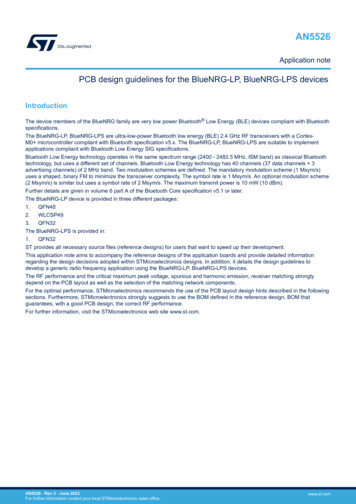
AN5526BlueNRG-LP/LPS matching network3BlueNRG-LP/LPS matching networkThe schematic below reports the suggested matching network. It presents the optimal impedance for Tx andRx performances and guarantees the harmonics filtering for Tx power up to the maximum level achievable byBlueNRG-LP, BlueNRG-LPS devices. It is composed of two cascaded pi networks with a notch filter for 2ndharmonic suppression that can be tuned adjusting the value of C2. The capacitor C5, placed at the end, ismandatory and cuts any DC current.The optimal impedance to be presented to the BlueNRG-LP, BlueNRG-LPS is 40 Ω and represents the righttrade-off for Tx and Rx performance. The matching network transforms this optimal impedance into 50 Ω.Two resistor footprints with overlapping pads can be used to realize a selector for either the antenna or a coaxialconnector placed on the board, avoiding stubs that could de-tune the network.A pi-network for antenna matching is usually foreseen and can be used to compensate de-tuning factors like thesurrounding materials.Figure 6. BlueNRG-LP/LPS matching network schematicThe reference matching network layout is shown below and some placement suggestions are also reported. Use a coplanar waveguide structureIt is highly recommended to place the first shunt capacitor as close as possible to the RF pin and isolate theGND pad from the top layer ground. Connect it to the inner layers to improve harmonic rejectionWhen necessary, taper the track from the RF pin to the first shunt capacitor to minimize discontinuities in thetrack width.Place at least one GND via close to each capacitor ground pad. Put vias along the RF pathUse 0201 or 0402 SMD componentsEnsure 50 Ω transmission line after the matching network.Figure 7. BlueNRG-LP/LPS matching network layoutAN5526 - Rev 3page 7/18
AN5526Layout recommendations4Layout recommendationsThe layout recommendations to follow during the development of a product based on the BlueNRG-LP, BlueNRGLPS are reported below. Put power supply decoupling capacitors as close as possible to VDD pins in order to reduce parasiticeffects. Always put the smallest capacitor first. Where possible, put more than one via close to the groundpad of the decoupling capacitorAlways ensure an uninterrupted ground area under the RF part and the decoupling capacitors in order toguarantee the shortest return path for high frequency currentsWhen the SMPS is used, care must be taken in the layout of the external components in order to minimizethe noise and unwanted couplings with the RF line (see Section 5.2 SMPS layout examples for layoutsuggestions)Minimize series parasitic inductance between ground pours of different layers putting as many stitching viasas possibleCreate a ring of stitching vias along the edges of the board to reduce radiation due to fringing fieldsEnsure optimum connection of the exposed pad of the QFN48 and QFN32 to the other ground layers. Use atleast a 4x4 matrix of ground vias (see Figure 8. BlueNRG-LP QFN48 exposed pad )The high-speed external crystal should be placed as close as possible to the OSCIN and OSCOUT pins tominimize wire parasitic capacitances and frequency shiftAvoid any routing under the high-speed crystal and close to OSCIN and OSCOUT pinsNo high-speed crystal external load capacitors are necessary. The frequency tuning is performed exploitingthe internal tuning network made by a fixed capacitor 6 binary weighted switchable ones. The effectiverange of loading capacitors are programmable through an internal register. The programmable register andthe capacitor range are reported in the BlueNRG-LP, BlueNRG-LPS datasheetsWhen possible, reserve the inner layers for most of the routing.Figure 8. BlueNRG-LP QFN48 exposed padAN5526 - Rev 3page 8/18
AN5526BlueNRG-LP/LPS layout examples5BlueNRG-LP/LPS layout examplesIn this section, the layout of different packages of the BlueNRG-LP, BlueNRG-LPS devices with the externalcomponents are presented. The proposed layouts cover two and four layer boards.Figure 9. BlueNRG-LP QFN48 - 2 layersFigure 10. BlueNRG-LPS QFN32 - 4 layersAN5526 - Rev 3page 9/18
AN5526BlueNRG-LP WLCSP routingFigure 11. BlueNRG-LPS QFN32 - 2 layers5.1BlueNRG-LP WLCSP routingThe layout of the BlueNRG-LP WLCSP is more complex than QFN. The BlueNRG-LP needs four layers to routeout all the signals. More layers, different technologies, and PCB classes can be used according to manufacturingcapabilities and the cost.A solution is presented below by using in pad stacked micro vias.Maximum micro via aspect ratio is 1:1. Considering a via hole size of 100 um, a board 400 um thick allowsbuilding stacked vias as represented below.A thicker board needs more advanced HDI technology.When the application does not route all signals, one level of micro via could be enough, reducing the cost of theboard.Figure 12. BlueNRG-LP WLCSP balls routing and stackupAN5526 - Rev 3page 10/18
AN5526SMPS layout examplesFigure 13. BlueNRG-LP WLCSP 4 layersIt is suggested that VSSRF and VSSIFADC are directly linked to the bottom layer and not to the top layer groundpour.Figure 14. BlueNRG-LP VSSRF and VSSIFADC connection5.2SMPS layout examplesThe DC-DC converter area is very sensitive and it is necessary to pay attention to the layout of this part. Thisis because the DC-DC converter generates noise that can get coupled on a surrounding ground, reducing thesensitivity and high frequency components that can be coupled onto the RF part.The general strategy is to make the switching current loop small and isolate the nodes carrying the noisy current.Most of the switching current is drained by the DC-DC converter output capacitor.To ensure a correct layout it is necessary:1.To provide efficient filtering by placing capacitors as close as possible to the BlueNRG-LP/LPSAN5526 - Rev 3page 11/18
AN5526SMPS layout examples2.3.To reduce parasitic inductance ensuring wide and short connections to the BlueNRG-LP/LPSTo use smaller inductor in series to the power inductor (see Figure 15. SMPS schematic ) to improve noisefiltering. If possible, put the two inductors orthogonal to each other to reduce the mutual coupling.Figure 15. SMPS schematicFigure 16. BlueNRG-LP QFN48 SMPS layoutAN5526 - Rev 3page 12/18
AN5526SMPS layout examplesFigure 17. BlueNRG-LP CSP49 SMPS layoutFigure 18. BlueNRG-LPS QFN32 SMPS layoutAN5526 - Rev 3page 13/18
AN5526Reference6Reference[1] BlueNRG-LP Datasheet (DS13282)[2] BlueNRG-LPS Datasheet (DS13819)AN5526 - Rev 3page 14/18
AN5526Revision historyTable 2. Document revision historyDateVersionChanges24-Jul-20201Initial release.15-Sep-20202Updated Section Introduction.Added references to the BlueNRG-LPS and related PCB design guidelines.13-Jun-20223Updated Figure 1. BlueNRG-LP QFN48 application board schematic,Figure 2. BlueNRG-LP WLCSP49 application board schematic, Figure 4. Twolayer application board stack-up, Figure 5. Four layer application board stackup.Added Section 3 BlueNRG-LP/LPS matching network, Section 4 Layoutrecommendations, Section 5 BlueNRG-LP/LPS layout examples,Section 5.1 BlueNRG-LP WLCSP routingSection 5.2 SMPS layoutexamples.AN5526 - Rev 3page 15/18
AN5526ContentsContents1Reference schematics . . . . . . . . . . . . . . . . . . . . . . . . . . . . . . . . . . . . . . . . . . . . . . . . . . . . . . . . . . . . . 22Two or more layer application board . . . . . . . . . . . . . . . . . . . . . . . . . . . . . . . . . . . . . . . . . . . . . . . 52.1Two layer solution . . . . . . . . . . . . . . . . . . . . . . . . . . . . . . . . . . . . . . . . . . . . . . . . . . . . . . . . . . . . . . 52.2More layer solution . . . . . . . . . . . . . . . . . . . . . . . . . . . . . . . . . . . . . . . . . . . . . . . . . . . . . . . . . . . . . 53BlueNRG-LP/LPS matching network . . . . . . . . . . . . . . . . . . . . . . . . . . . . . . . . . . . . . . . . . . . . . . . 74Layout recommendations . . . . . . . . . . . . . . . . . . . . . . . . . . . . . . . . . . . . . . . . . . . . . . . . . . . . . . . . . . 85BlueNRG-LP/LPS layout examples . . . . . . . . . . . . . . . . . . . . . . . . . . . . . . . . . . . . . . . . . . . . . . . . . 965.1BlueNRG-LP WLCSP routing . . . . . . . . . . . . . . . . . . . . . . . . . . . . . . . . . . . . . . . . . . . . . . . . . . . 105.2SMPS layout examples . . . . . . . . . . . . . . . . . . . . . . . . . . . . . . . . . . . . . . . . . . . . . . . . . . . . . . . . 11Reference . . . . . . . . . . . . . . . . . . . . . . . . . . . . . . . . . . . . . . . . . . . . . . . . . . . . . . . . . . . . . . . . . . . . . . . .14Revision history . . . . . . . . . . . . . . . . . . . . . . . . . . . . . . . . . . . . . . . . . . . . . . . . . . . . . . . . . . . . . . . . . . . . . . .15AN5526 - Rev 3page 16/18
AN5526List of figuresList of figuresFigure 1.Figure 2.Figure 3.Figure 4.Figure 5.Figure 6.Figure 7.Figure 8.Figure 9.Figure 10.Figure 11.Figure 12.Figure 13.Figure 14.Figure 15.Figure 16.Figure 17.Figure 18.AN5526 - Rev 3BlueNRG-LP QFN48 application board schematic. . .BlueNRG-LP WLCSP49 application board schematicBlueNRG-LPS QFN32 application board schematic. .Two layer application board stack-up . . . . . . . . . . . .Four layer application board stack-up . . . . . . . . . . .BlueNRG-LP/LPS matching network schematic . . . .BlueNRG-LP/LPS matching network layout . . . . . . .BlueNRG-LP QFN48 exposed pad . . . . . . . . . . . . .BlueNRG-LP QFN48 - 2 layers . . . . . . . . . . . . . . . .BlueNRG-LPS QFN32 - 4 layers . . . . . . . . . . . . . . .BlueNRG-LPS QFN32 - 2 layers . . . . . . . . . . . . . . .BlueNRG-LP WLCSP balls routing and stackup . . . .BlueNRG-LP WLCSP 4 layers . . . . . . . . . . . . . . . .BlueNRG-LP VSSRF and VSSIFADC connection . . .SMPS schematic . . . . . . . . . . . . . . . . . . . . . . . . .BlueNRG-LP QFN48 SMPS layout . . . . . . . . . . . . .BlueNRG-LP CSP49 SMPS layout . . . . . . . . . . . . .BlueNRG-LPS QFN32 SMPS layout . . . . . . . . . . . . 2. 3. 3. 5. 5. 7. 7. 8. 9. 91010111112121313page 17/18
AN5526IMPORTANT NOTICE – READ CAREFULLYSTMicroelectronics NV and its subsidiaries (“ST”) reserve the right to make changes, corrections, enhancements, modifications, and improvements to STproducts and/or to this document at any time without notice. Purchasers should obtain the latest relevant information on ST products before placing orders. STproducts are sold pursuant to ST’s terms and conditions of sale in place at the time of order acknowledgment.Purchasers are solely responsible for the choice, selection, and use of ST products and ST assumes no liability for application assistance or the design ofpurchasers’ products.No license, express or implied, to any intellectual property right is granted by ST herein.Resale of ST products with provisions different from the information set forth herein shall void any warranty granted by ST for such product.ST and the ST logo are trademarks of ST. For additional information about ST trademarks, refer to www.st.com/trademarks. All other product or service namesare the property of their respective owners.Information in this document supersedes and replaces information previously supplied in any prior versions of this document. 2022 STMicroelectronics – All rights reservedAN5526 - Rev 3page 18/18
In addition, it details the design guidelines to develop a generic radio frequency application using the BlueNRG-LP, BlueNRG-LPS devices. The RF performance and the critical maximum peak voltage, spurious and harmonic emission, receiver matching strongly depend on the PCB layout as well as the selection of the matching network components.