Transcription
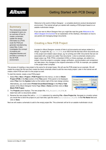
Getting Started with PCB DesignSummaryThis introductory tutorialis designed to give youan overview of how tocreate a schematic,update the designinformation to a PCB,route the PCB andgenerate manufacturingoutput files. It alsoinvestigates the conceptof projects andintegrated libraries andprovides a summary ofthe 3D PCBenvironment.Welcome to the world of Altium Designer – a complete electronic product developmentenvironment. This tutorial will get you started with creating a PCB project based on anastable multivibrator design.If you are new to Altium Designer then you might like read the guide Welcome to theAltium Designer Environment for an explanation of the interface, information on how touse panels and managing design documents.Creating a New PCB ProjectA project in Altium Designer consists of links to all documents and setups related to adesign. A project file, eg. xxx.PrjPCB, is an ASCII text file that lists which documents arein the project and related output setups, eg. for printing and CAM. Documents that are notassociated with a project are called ‘free documents’. Links to schematic sheets and atarget output, eg. PCB, FPGA, embedded (VHDL) or library package, are added to aproject. Once the project is compiled, design verification, synchronization and comparisoncan take place. Any changes to the original schematics or PCB, for example, are updatedin the project when compiled.The process of creating a new project is the same for all project types. We will use the PCB project as an example. We willcreate the project file first and then create the blank schematic sheet to add the new empty project. Later in this tutorial we willcreate a blank PCB and add it to the project as well.To start the tutorial, create a new PCB project:1. Select File » New » Project » PCB Project from the menus, or click on BlankProject (PCB) in the New section of the Files panel. If this panel is not displayed,select Files from the System button at the bottom right of the main design window.Alternatively, you could select Printed Circuit Board Design in the Pick a Tasksection of the Altium Designer Home Page (View » Home) and then click on NewBlank PCB Project.2. The Projects panel displays. The new project file, PCB Project1.PrjPCB, islisted here with no documents added.3. Rename the new project file (with a .PrjPCB extension) by selecting File » Save Project As. Navigate to a location whereyou would like to store the project on your hard disk, type the name Multivibrator.PrjPCB in the File Name field andclick on Save.Next we will create a schematic to add to the empty project file. This schematic will be for an astable multivibrator circuit.Version (v2.3) May 21, 20081
TU0117 Getting Started with PCB DesignCreating a New Schematic SheetCreate a new schematic sheet by completing the following steps:1. Select File » New » Schematic, or click on Schematic Sheet in the New section of the Files panel. A blank schematicsheet named Sheet1.SchDoc displays in the design window and the schematic document is automatically added (linked)to the project. The schematic sheet is now listed under Source Documents beneath the project name in the Projects tab.2. Rename the new schematic file (with a .SchDoc extension) by selecting File » Save As. Navigate to a location where youwould like to store the schematic on your hard disk, type the name Multivibrator.SchDoc in the File Name field andclick on Save.When the blank schematic sheet opens you will notice that the workspace changes. The main toolbar includes a range of newbuttons, new toolbars are visible, the menu bar includes new items and the Sheet panel is displayed. You are now in theSchematic Editor.You can customize many aspects of the workspace. For example, you can reposition the panels and toolbars or customize themenu and toolbar commands.Now we can add our blank schematic to the project before proceeding with the design capture.Adding Schematic Sheets to a ProjectIf the schematic sheets you want to add to a project file have been opened as Free Documents, right-click on the project namein the Projects panel and select Add Existing to Project. Select the free documents name(s) and click Open. Alternatively,you could drag-and-drop the free document into the project documents list in the Projects panel. The schematic sheet is nowlisted under Source Documents beneath the project name in the Projects tab and is linked to the project file.Version (v2.3) May 21, 20082
TU0117 Getting Started with PCB DesignSetting the Schematic OptionsThe first thing to do before you start drawing your circuit is to set up the appropriate document options.Complete the following steps.1. From the menus, choose Design » Document Options and the Document Options dialog will open.For this tutorial, the only change we need to make here is to set the sheet size to standard A4 format.In the Sheet Options tab, find the Standard Styles field. Click the arrow next to the entry to see alist of sheet styles.2. Select the A4 style and click OK to close the dialog and update the sheet size.3. To make the document fill the viewing area again, select View » Fit Document.Altium Designer has amultilevel Undo, allowingyou to undo any numberof previous actions. Themaximum number ofUndo steps is userconfigurable and limitedonly by the availablememory on yourcomputer.In Altium Designer, you can activate any menu by pressing the menu hotkey (the underlined letter in themenu name). Any subsequent menu items will also have hot keys that you can use to activate the item. For example, theshortcut for selecting the View » Fit Document menu item is to press the V key followed by the D key. Many submenus, suchas the Edit » DeSelect menu, can be called directly. To activate the Edit » DeSelect » All on Current Document menu item,you need only press the X key (to call up the DeSelect menu directly) followed by the S key.Next we will set the general schematic preferences.1. Select Tools » Schematic Preferences [shortcut: T, P] to open the schematic Preferences dialog.This dialog allows you to set global preferences that will apply to all schematic sheets you work on.2. Click on Schematic – Default Primitives in the selection tree (left side of the dialog) to make it theactive page and enable the Permanent option. Click OK to close the dialog.3. Before you start capturing your schematic, save this schematic sheet, so select File » Save[shortcut: F, S].You can save anyschematic sheet as adocument template(.schdot) allowing you toinclude specialinformation such as acustom company titleblock and logo.Drawing the SchematicYou are now ready to begin capturing (drawing) the schematic. For this tutorial, we will use the circuit shown in Figure 1. Thiscircuit uses two 2N3904 transistors configured as a self-running astable multivibrator.Figure 1. An astable multivibrator.Version (v2.3) May 21, 20083
TU0117 Getting Started with PCB DesignLocating the Component and Loading the LibrariesTo manage the thousands of schematic symbols included with Altium Designer, the Schematic Editor provides powerful librarysearch features. Although the components we require are in the default installed libraries, it is useful to know how to searchthrough the libraries to find components. Work through the following steps to locate and add the libraries you will need for thetutorial circuit.First we will search for the transistors, both of which are type2N3904.1. Click on the Libraries tab to display the Libraries panel.2. Press the Search button in the Libraries panel, or selectTools » Find Component, to open the Libraries Searchdialog.3. Ensure that Search in dropdown in the Options region isset to Components for this example. There are otheroptions for library searching using different criteria.4. Ensure that the Scope is set to Libraries on Path andthat the Path field contains the correct path to yourlibraries. If you accepted the default directories duringinstallation, the path should be the Library folder ofyour Altium Designer installation. Click on the folder iconto browse to the library folder. Ensure that the IncludeSubdirectories box is not selected (not ticked) for thisexample.5. We want to search for all references to 3904, so type 3904 in the Value field of the first Filters row at the top of theLibraries Search dialog, and set the Operator to contains.6. Click the Search button to begin the search. The Query Results are displayed in the Libraries panel as the search takesplace.7. Click on the component name 2N3904 found in the Miscellaneous Devices.IntLiblibrary to select it. This library has symbols for all the available simulation-ready BJTtransistors.8. If you choose a component that resided in a library that was not currently installed, you areasked to confirm the installation of that library before you could place the component onyour schematic. Since the Miscellaneous Devices library is already installed by default, thecomponent is ready to place.The added libraries will appear in the drop down list at the top of the Libraries panel. As youclick on a library name in the upper list, the components in that library are listed below. Thecomponent filter in the panel can then be used to quickly locate a component within a library.Placing the Components on Your SchematicThe first components we will place on the schematic are the two transistors, Q1 and Q2. Forthe general layout of the circuit, refer to the schematic drawing shown in Figure 1.1. Select View » Fit Document [shortcut: V, D] to ensure your schematic sheet takes up thefull window.2. Make sure the Libraries panel is displayed by clicking on the Libraries tab.3. Q1 and Q2 are BJT transistors, so select the Miscellaneous Devices.IntLib libraryfrom the Libraries drop-down list at the top of the Libraries panel to make it the activelibrary.4. Use the filter to quickly locate the component you need. The default wildcard (*) will list allcomponents found in the library. Set the filter by typing *3904 in the filter field below theLibrary name. A list of components which have the text “3904” as part of their Component Name field will be displayed.Version (v2.3) May 21, 20084
TU0117 Getting Started with PCB Design5. Click on the 2N3904 entry in the list to select it, then click the Place button. Alternatively, just double-click on the componentname. The cursor will change to a cross hair and you will have an outlined version of the transistor “floating” on your cursor.You are now in part placement mode. If you move the cursor around, the transistor outline will move with it.6. Before placing the part on the schematic, first edit its properties. While the transistor is floating on the cursor, press the TABkey. This opens the Component Properties dialog for the component. We will now set up the dialog options to appear asbelow.The link between theschematic componentand the PCBcomponent is thefootprint name. Thefootprint specified in theschematic is loadedfrom the PCB librarywhen you transfer thedesign to the PCBeditor. Double-click ona schematic componentto specify the footprint.7. In the Properties section of the dialog, set the value for the first component designator by typing Q1 in the Designator field.8. Next we will check the footprint that will be used to represent the component in the PCB. For this tutorial, we have usedintegrated libraries which mean that the recommended models for footprints and circuit simulation are already included.Make sure that footprint name TO-92A is included in the Models list. Leave all other fields at their default values and clickOK to close the dialog.You are now ready to place the part.1. Move the cursor (with the transistor symbol attached) to position the transistor a little tothe left of the middle of the sheet. Once you are happy with the transistor’s position,click or press ENTER to place the transistor onto the schematic.2. Move the cursor and you will find that a copy of the transistor has been placed on theschematic sheet, but you are still in part placement mode with the part outline floatingon the cursor. This feature of Altium Designer allows you to place multiple parts of thesame type. So let’s now place the second transistor. This transistor is the same as theprevious one, so there is no need to edit its attributes before we place it. AltiumDesigner will automatically increment a component’s designator when you place aseries of parts. In this case, the next transistor we place will automatically bedesignated Q2.When you are in any editing or placementmode (a cross hair cursor is active),moving the cursor to the edge of thedocument window will automatically panthe document.If you accidentally pan too far while youare wiring up your circuit, press V, F (View» Fit All Objects) to redraw the schematicwindow, showing all placed objects. Thiscan be done even when you are in themiddle of placing an object.3. If you refer to the schematic diagram (Figure 1) you will notice that Q2 is drawn as a mirror of Q1.To flip the orientation of the transistor that is floating on the cursor, press the X key. This flips thecomponent horizontally.4. Move the cursor to position the part to the right of Q1. To position the component moreaccurately, press the PAGE UP key twice to zoom in two steps. You should now be able to seethe grid lines.Version (v2.3) May 21, 2008Use the following keys tomanipulate the part floatingon the cursor:- Y flips the part vertically- X flips the part horizontally- Spacebar rotates the partby 90 anti-clockwise.5
TU0117 Getting Started with PCB Design5. Once you have positioned the part, click or press ENTER to place Q2. Once again a copy of the transistor you are “holding”will be placed on the schematic, and the next transistor will be floating on the cursor ready to be placed.6. Since we have now placed all the transistors, we will exit part placement mode by clicking the right mouse button or pressingthe ESC key. The cursor will revert back to a standard arrow.Next we will place the four resistors.1. In the Libraries panel, make sure the Miscellaneous Devices.IntLib library is active.2. Set the filter by typing res1 in the filter field below the Library name.3. Click on Res1 in the components list to select it, then click the Place button. You will now havea resistor symbol floating on the cursor.To edit the attributes of anobject placed on theschematic, double-click theobject to open its ComponentProperties dialog.4. Press the TAB key to edit the resistor’s attributes. In the Properties section of the dialog, setthe value for the first component designator by typing R1 in the Designator field.5. Make sure that footprint name AXIAL-0.3 is included in the Models list.6. The contents of Comment field of the schematic component maps to the Comment field of the PCB component, typicallyyou would enter the value or the resistor here. Enter a value of 100k into the Comment field for R1.Components being simulated may have a number of simulation properties that can be defined (eg, a resistor has 1, a BJT has 5, and a MOSFET has13), these properties are defined by using Parameters. If you wanted to simulate this circuit then the resistor value must be defined as a Parameter,whose name is Value and whose value is the resistance.If the circuit being captured is for both simulation and PCB layout, rather than enter the value twice (in the parameter called Value and then in theComment field), Altium Designer supports ‘indirection’, a feature that maps any parameter’s string into the Comment field. If you click to display theComment field dropdown list you will see that the software has automatically built a list of all current parameters, in case you want to map the value ofone of them into the Comment field.7. Since you will not be simulating ensure that the Visible option for the Value parameter is disabled.8. Click OK to close the dialog.9. Press the SPACEBAR to rotate the resistor by 90 so it is in the correct orientation.10. Position the resistor above the base of Q1 (refer to the schematic diagram in Figure 1) and click or press ENTER to placethe part. Don’t worry about making the resistor connect to the transistor just yet. We will wire up all the parts later.11. Next place the other 100k resistor R2 above the base of Q2. The designator will automatically increment when you place thesecond resistor.12. The remaining two resistors, R3 and R4, have a value of 1k, so press the TAB key to open the Component Propertiesdialog, enter 1k into the Comment, and confirm that the Visible option for the Value parameter is disabled. Click OK toclose the dialog.13. Position and place R3 and R4 as shown in the schematic diagram in Figure 1. Right-click or press ESC to exit partplacement mode.Now place the two capacitors.1. The capacitor part is also in the Miscellaneous Devices.IntLib library, which shouldalready be selected in the Libraries panel.2. Type cap in the component’s filter field in the Libraries panel.3. Click on CAP in the components list to select it, then click the Place button. You will now have acapacitor symbol floating on the cursor.4. Press the TAB key to edit the capacitor’s attributes. In the Component Properties dialog set theDesignator to C1, the Comment to 20n, disable the Visible option for the Value parameter,and check the PCB footprint model RAD-0.3 is selected in the Models list. Click OK.To reposition any object, placethe cursor directly over theobject, click-and-hold the leftmouse button, drag the objectto a new position and thenrelease the mouse button.As with the resistor, if you wanted to simulate this circuit you would need a Value parameter with the value of 20n, in thiscase you would define the capacitance in the Value parameter and then use the indirection feature to map the contents ofthe value parameter into the Comment field. Since you will not be simulating ensure that the Visible option for the Valueparameter is disabled.5. Position and place the two capacitors in the same way that you placed the previous parts.6. Right-click or press ESC to exit placement mode.The last component to be placed is the connector, located in Miscellaneous Connectors.IntLib.Version (v2.3) May 21, 20086
TU0117 Getting Started with PCB Design1. Select Miscellaneous Connectors.IntLib from the Libraries list in the Libraries panel. The connector we want is atwo-pin socket, so set the filter to *2*.2. Select Header 2 from the parts list and click the Place button. Press TAB to edit the attributes and set Designator to Y1 andcheck the PCB footprint model is HDR1X2. No Value parameter is required as you would replace this component with apower source when simulating the circuit. Click OK to close the dialog.3. Before placing the connector, press X to flip it horizontally so that it is in the correct orientation. Click to place the connectoron the schematic.4. Right-click or press ESC to exit part placement mode.5. Save your schematic by selecting File » Save from the menus [shortcut: F, S].You have now placed all the components. Note that the components in Figure 2 are spaced so that there is plenty of room towire to each component pin. This is important because you cannotplace a wire across the bottom of a pin to get to a pin beyond it. If youYou can re-position a group of selected schematic objects using thedo, both pins will connect to the wire.If you need to move a component, click-and-hold on the body of thecomponent, then drag the mouse to reposition it.arrow keys. The movement of selected objects are set according tothe current Snap Grid setting in the Document Options dialog(Document » Options [shortcut: D,O]). You can use this dialog tochange the Snap Grid Value. This Grid value also appears on theStatus bar of Altium Designer.The Schematic – Grids page of the Preferences dialog (Tools »Schematic Preferences [shortcut: T, P]) can also be used to setimperial and metric grid presets. Use the G shortcut to cycle throughdifferent snap grid setting values. You can also use the View » Gridssubmenu or the Grids right-click menu.Selected objects can be 'nudged' by small amounts (by the currentsnap grid value) by pressing the arrow keys while holding down theCTRL key.Selected objects can also be 'nudged' by large amounts (the snapgrid value by a factor of 10) by pressing the arrow keys whileholding down the CTRL and SHIFT keys together.Figure 2. Schematic with all parts placed.Wiring up the CircuitWiring is the process of creating connectivity between the various components of your circuit. To wire up your schematic, referto the diagram in Figure 1 and complete the following steps.1. To make sure you have a good view of the schematic sheet, use the PAGE UP key tozoom in or PAGE DOWN to zoom out. Also try holding down the CTRL key and usingthe mouse wheel to zoom or holding the mouse wheel down and dragging the mouse upto zoom in or down to zoom out.2. Firstly wire the resistor R1 to the base of transistor Q1 in the following manner. SelectPlace » Wire [shortcut: P, W] from the menus or click on the Wire tool on the Wiringtoolbar to enter the wire placement mode. The cursor will change to a crosshair.3. Position the cursor over the bottom end of R1. When you are in the right position, a redconnection marker (large asterisk) will appear at the cursor location. This indicates thatthe cursor is over an electrical connection point on the component.4. Click or press ENTER to anchor the first wire point. Move the cursor and you will see awire extend from the cursor position back to the anchor point.5. Position the cursor so that it is below R1 and level with the base of Q1. Click or pressENTER to anchor the wire at this point. The wire between the first and second anchorpoints will be placed.To graphically edit the shape of a wire,or any other graphical object once it hasbeen placed, position the arrow cursorover it and click once.Whenever a wire runs across theconnection point of a component, or isterminated on another wire, AltiumDesigner will automatically create ajunction.When placing wires, keep in mind thefollowing points:- click or press ENTER to anchor thewire at the cursor position;- press BACKSPACE to remove the lastanchor point;6. Position the cursor over the base of Q1 until you see the cursor change to a redconnection marker. Click or press ENTER to connect the wire to the base of Q1.- after placing the last segment of awire, right-click or press ESC to endthe wire placement. The cursor willremain as a cross hair and you canbegin placing another wire.7. Note that the cursor remains a cross hair, indicating that you are ready to place anotherwire. To exit placement mode completely and go back to the arrow cursor, you would- Right-click again or press ESC to exitwire placement mode.Version (v2.3) May 21, 20087
TU0117 Getting Started with PCB Designright-click or press ESC again – but don’t do this just now.8. We will now wire C1 to Q1 and R1. Position the cursor over the left connection point of C1 and click or press ENTER to starta new wire. Move the cursor horizontally till it is directly over the wire connecting the base of Q1 to R1. A connection markerwill appear. Click or press ENTER to place the wire segment, then right-click or press ESC to indicate that you have finishedplacing the wire. Note how the two wires are automatically connected.9. Wire up the rest of your circuit, as shown in Figure 3.A wire that crosses the end of apin will connect to that pin, evenif you delete the junction. Checkthat your circuit looks like Figure3 before proceeding.Figure 3. The fully wired schematic.10. When you have finished placing all the wires, right-click or press ESC to exit placement mode. The cursor will revert to anarrow.11. If you wish to move any placed components and drag any connected wires with it, hold down the CTRL key while movingthe component, or select Move » Drag.Nets and Net LabelsEach set of component pins that you have connected to each other now form what is referred to as a net. For example, one netincludes the base of Q1, one pin of R1 and one pin of C1.To make it easy to identify important nets in the design, you can add net labels. To place net labels on the two power nets:1. Select Place » Net Label [shortcut: P, N]. A dotted box will appear floating on the cursor.2. To edit the net label before it is placed, press the TAB key to display the Net Label dialog.3. Type 12V in the Net field, then click OK to close the dialog.4. Place the net label so that the bottom left of the net label touches the upper most wire on the schematic. Thecursor will change to a red cross when the net label touches the wire. If the cross is light gray, it means youare trying to label a pin instead.5. After placing the first net label you will still be in net label placement mode, so press the TAB key again to edit the secondnet label before placing it.6. Type GND in the Net field, click OK to close the dialog and place the net label.7. Place the net label so that the bottom left of the net label touches the lower most wire on the schematic. Right-click or pressESC to exit net label placement mode.8. Select File » Save [shortcut: F, S] to save your circuit. Save the project as well.Congratulations! You have just completed your first schematic capture using Altium Designer.Before we turn the schematic into a circuit board, let’s set up the project options.Version (v2.3) May 21, 20088
TU0117 Getting Started with PCB DesignSetting Up Project OptionsThe project options include the error checking parameters, a connectivity matrix, Class Generator, the Comparator setup, ECOgeneration, output paths and netlist options, Multi-Channel naming formats, Default Print setups, Search Paths and any projectparameters you wish to specify. Altium Designer will use these setups when you compile the project.When a project is compiled, comprehensive design and electrical rules are applied to verify the design. When all errors areresolved, the re-compiled schematic designs are loaded into the target document, eg. a PCB document, by generated ECOs.The project Comparator allows you to finddifferences between source and target filesand update (synchronize) in both directions.All project-related operations, such as errorchecking, comparing documents and ECOgeneration, are set up in the Options forProject dialog (Project » Project Options).Project outputs, such as assembly andfabrication outputs and reports can be set upfrom the File menu options. You can also setup job options in an Output Job file (File »New » Output Job File). See Setting Up theProject Outputs for more information.1. Select Project » Project Options. TheOptions for Project dialog opens.2. Set up any project-related options in thisdialog. We will now make some changes tothe Error Reporting, Connection Matrixand Comparator tabs.Checking the Electrical Properties of Your SchematicSchematic diagrams in Altium Designer are more than just simple drawings – they contain electrical connectivity informationabout the circuit. You can use this connectivity awareness to verify your design. When you compile a project, Altium Designerchecks for errors according to the rules set up in the Error Reporting and Connection Matrix tabs and any violationsgenerated will display in the Messages panel.Setting Up Error ReportingThe Error Reporting tab in the Options for Project dialog is used to set up design draftingchecks. The Report Mode settings show the levelof severity of a violation. If you wish to change asetting, click on a Report Mode next to the violationyou wish to change and choose the level of severityfrom the drop-down list. For this tutorial we will usethe default settings.Setting Up the Connection MatrixThe Connection Matrix tab (Options for Projectdialog) displays the severity of an error type that isproduced when error reporting is run to checkelectrical connections within the design, i.e.connections between pins, ports and sheet entries.The matrix gives a graphical representation ofdifferent types of connection points on a schematicand whether they are allowable or not.Version (v2.3) May 21, 20089
TU0117 Getting Started with PCB DesignFor example, look down the entries on the right side of the matrix diagram and find Output Pin. Read across this row of thematrix till you get to the Open Collector Pin column. The square where they intersect is orange indicating that an Output Pinconnected to an Open Collector Pin on your schematic will generate an error condition when the project is compiled.You can set each error type with a separate error level, eg. from no report at all through to a fatal error. Right-click to see themenu options to control the entire matrix.To make changes to the Connection Matrix:1. Click on the Connection Matrix tab in the Options for Project dialog.2. Click on the box that is at the intersection of two types of connection, eg. Output Sheet Entry and Open Collector Pin.3. Click until the box changes to the color of the errors as listed in the legend, eg. an orange box indicates that an error will begenerated if such a connection is found.Our circuit contains only Passive Pins (on resistors, capacitors and the connector) and Input Pins (on the transistors. Let’s checkto see if the connection matrix will detect unconnected passive pins.1. Look down the row labels to find Passive Pin. Look across the column labels to find Unconnected. The square where theseentries intersect indicates the error condition when a passive pin is found to be unconnected in the schematic. The default isa green square, which indicates that no report will be generated.2. Click on this intersection box until it turns yellow, so that a warning will be generated for unconnected passive pins when wecompile the project. We will purposely create an instance of this error to check it later in this tutorial.Setting Up the ComparatorThe Comparator tab in the Options for Project dialog se
A project in Altium Designer consists of links to all documents and setups related to a design. A project file, eg. xxx.PrjPCB, is an ASCII text file that lists which documents are in the project and related output setups, eg. for printing and CAM. Documents that are not associated with a project are called 'free documents'.

