Transcription
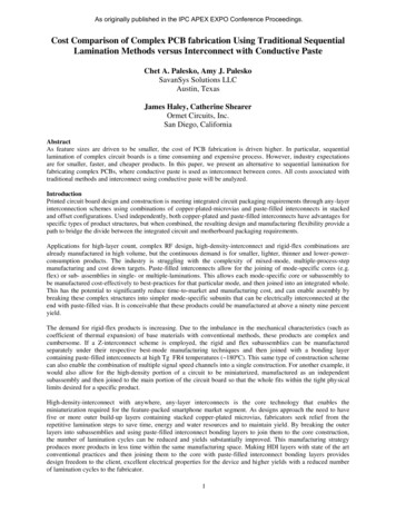
As originally published in the IPC APEX EXPO Conference Proceedings.Cost Comparison of Complex PCB fabrication Using Traditional SequentialLamination Methods versus Interconnect with Conductive PasteChet A. Palesko, Amy J. PaleskoSavanSys Solutions LLCAustin, TexasJames Haley, Catherine ShearerOrmet Circuits, Inc.San Diego, CaliforniaAbstractAs feature sizes are driven to be smaller, the cost of PCB fabrication is driven higher. In particular, sequentiallamination of complex circuit boards is a time consuming and expensive process. However, industry expectationsare for smaller, faster, and cheaper products. In this paper, we present an alternative to sequential lamination forfabricating complex PCBs, where conductive paste is used as interconnect between cores. All costs associated withtraditional methods and interconnect using conductive paste will be analyzed.IntroductionPrinted circuit board design and construction is meeting integrated circuit packaging requirements through any-layerinterconnection schemes using combinations of copper-plated-microvias and paste-filled interconnects in stackedand offset configurations. Used independently, both copper-plated and paste-filled interconnects have advantages forspecific types of product structures, but when combined, the resulting design and manufacturing flexibility provide apath to bridge the divide between the integrated circuit and motherboard packaging requirements.Applications for high-layer count, complex RF design, high-density-interconnect and rigid-flex combinations arealready manufactured in high volume, but the continuous demand is for smaller, lighter, thinner and lower-powerconsumption products. The industry is struggling with the complexity of mixed-mode, multiple-process-stepmanufacturing and cost down targets. Paste-filled interconnects allow for the joining of mode-specific cores (e.g.flex) or sub- assemblies in single- or multiple-laminations. This allows each mode-specific core or subassembly tobe manufactured cost-effectively to best-practices for that particular mode, and then joined into an integrated whole.This has the potential to significantly reduce time-to-market and manufacturing cost, and can enable assembly bybreaking these complex structures into simpler mode-specific subunits that can be electrically interconnected at theend with paste-filled vias. It is conceivable that these products could be manufactured at above a ninety nine percentyield.The demand for rigid-flex products is increasing. Due to the imbalance in the mechanical characteristics (such ascoefficient of thermal expansion) of base materials with conventional methods, these products are complex andcumbersome. If a Z-interconnect scheme is employed, the rigid and flex subassemblies can be manufacturedseparately under their respective best-mode manufacturing techniques and then joined with a bonding layercontaining paste-filled interconnects at high Tg FR4 temperatures ( 180ºC). This same type of construction schemecan also enable the combination of multiple signal speed channels into a single construction. For another example, itwould also allow for the high-density portion of a circuit to be miniaturized, manufactured as an independentsubassembly and then joined to the main portion of the circuit board so that the whole fits within the tight physicallimits desired for a specific product.High-density-interconnect with anywhere, any-layer interconnects is the core technology that enables theminiaturization required for the feature-packed smartphone market segment. As designs approach the need to havefive or more outer build-up layers containing stacked copper-plated microvias, fabricators seek relief from therepetitive lamination steps to save time, energy and water resources and to maintain yield. By breaking the outerlayers into subassemblies and using paste-filled interconnect bonding layers to join them to the core construction,the number of lamination cycles can be reduced and yields substantially improved. This manufacturing strategyproduces more products in less time within the same manufacturing space. Making HDI layers with state of the artconventional practices and then joining them to the core with paste-filled interconnect bonding layers providesdesign freedom to the client, excellent electrical properties for the device and higher yields with a reduced numberof lamination cycles to the fabricator.1
Every layer interconnection (ELIC) and subassembly core to core interconnects are delivering: Tighter wring densities Improved performance through shorter traces Separation of low and high speed signal channels Ability to join different materials in optimum press cycles A framework for embedded componentsThese assembly advantages, coupled with proper design, offer cost advantages when products are built in large-scaleproduction or in low volume, high mix assembly lines. It is the intent of this paper to outline the costs associatedwith manufacturing ELIC structures employing a Z-interconnect paste technology. Two example designs werechosen to analyze the cost of using this technology versus conventional interconnect. The first case is a small 10layer board similar to most smart phone motherboards. The second case is a large 28 layer circuit board similar tothose found in servers.Activity Based Cost ModelingActivity based cost modeling and parametric cost modeling are the two dominant cost modeling methods.Parametric cost modeling is done by statistically analyzing a large number of actual results and creating a model thatmatches as closely as possible. This “black box” approach, as an extrapolation based on historical data, is onlyappropriate for modeling processes that change slowly over time or cannot be decomposed into individual activities.For reliable and dynamic trade-offs, activity based cost modeling is the most accurate cost modeling method becauseindividual activities are characterized and analyzed. The total cost of any manufacturing process is calculated bydividing the process into a series of activities and totaling the cost of each activity. The cost of each activity isdetermined by analyzing the following attributes: The time required to complete the activityThe amount of labor dedicated to the activityThe cost of material required to perform that activity—both consumable and permanent materialAny tooling costThe depreciation cost of the equipment required to perform the activityThe yield loss associated with the activityActivity based cost modeling is also well suited to comparing different technologies and manufacturing processes.The total cost of a product can be divided into the following three categories: Direct manufacturing costAllocated factory overheadProfit marginThe direct manufacturing cost is easy to quantify and reasonably consistent across the industry. However, factoryoverhead and profit margin vary significantly between different manufacturing sites and companies. By usingactivity based cost modeling, the specific differences in manufacturing cost can be determined by comparing thedirect manufacturing costs. This “relative” cost modeling makes it much easier to understand the cost impacts—good or bad—of design decisions and technology tradeoffs.The graph in Figure 1 shows a partial example of an activity based cost graph for a high density interconnect (HDI)PCB substrate. Each activity contributes cost in at least one of the six categories shown. These categories arerepresented by the colored bars, and the running total is the line on the graph. The example shows the first series ofactivities in the fabrication process.
Figure 1. Example of Activity Based Cost ModelingThe inner layer core and HDI buildup activities contribute significant material costs, as shown by the blue bars forthose two steps. Any type of via drilling—either laser or mechanical—will contribute capital costs since thethroughput per panel is usually low. Many of the other activities contribute labor and equipment depreciation costs,as shown by the orange and purple bars.Conductive Paste InterconnectConductive pastes are commonly used to make electronic interconnects and printed circuits. They come in severalvariations, ranging from Nano silver to epoxy-based metal fillers. They serve several markets and have been used incommercial and high reliability applications. Most are air-cured formulations and may display a wide discrepancy inelectrical resistance.Conductive paste can be used in printed circuit board fabrication as an alternative to copper plated vias. Theconductive paste vias are created by laser drilling holes in a prepreg layer. A screen printing process is used to fillthese holes with conductive paste and then the panel is heated and cured to sinter the paste. At this point, the corewith the conductive paste vias (Z-interconnect layer) can be included in the normal PCB layup and press laminationprocess.Sintering is a process in which adjacent surfaces of metal powder particles are bonded by heating. Liquid phasesintering is a special form of sintering during which solid powder particles coexist with a liquid phase. Densificationand homogenization of the mixture occur as the metals diffuse into one another and form new alloys and/orintermetallic species.In Transient Liquid Phase Sintering (TLPS), compositions comprising powder metallurgy, a relatively low meltingpoint (LMP) alloy and a relatively high melting point (HMP) metal are mixed in particulate form. At least oneelement within the alloy is either highly soluble in, or is reactive with, the receptive HMP metal. As the temperatureis raised to the melting point of the LMP alloy, the alloy particles become molten. This transition can be observed asan endothermic event in differential scanning calorimetry (DSC). The reactive elements within the relatively lowmelting point alloy then react with the receptive high melting point metal to form new alloy compositions and/orintermetallic compounds. The formation of intermetallic species may be observed as an exothermic event usingDSC. Thus, the typical TLPS DSC “signature” is an endotherm followed by an exothermic phase. The diffusion andreaction of the reactive elements from the LMP alloy and the receptive HMP metal continues until one of thereactants is fully depleted, there is no longer a molten phase at the process temperature, or the reaction is quenchedby cooling. After cooling, subsequent temperature excursions (even beyond the original LMP alloy melttemperature) do not reproduce the original melt signature of the mixture. This is the “signature” of a typical lowtemperature transient liquid phase sintered metal mixture.
Cost Modeling ResultsAs part of this project, the total costs of the following two scenarios were analyzed using proprietary activity basedcost modeling software described in the previous section.Case 1 – Mobile phone boardThis printed circuit board uses a 10 layer high density interconnect (HDI) structure. The board is 2 inches by 2.5inches, and is similar in size and complexity to a smart phone motherboard. Using traditional HDI fabrication, thisboard would be a 4-2-4 structure—a 2 layer core with four sequential buildup layers on the top and bottom. Usingthe proprietary Z-interconnect technology, this board could be constructed using 5 cores and 4 Z-interconnect layers.The cross section of each option is shown in Figure 2 below.PrePregCoreOrmetConductivePaste4-2-4 HDI Structure5 Core Z-interconnect StructureFigure 2. Cross section of a 4-2-4 board and a 5 core Z-interconnect boardThe traditional HDI board is built by starting with a copper clad laminate core. The copper on this core is patternedon both sides, and through holes are drilled for the core vias. These through holes are plated to complete the coreprocessing. Then, four HDI build up processes are done, including lamination, laser drilling of the vias, imaging,and electroplating. These processes are done sequentially, and the board is completed with a surface finish andsolder mask process.The 5 core Z-interconnect process uses five cores instead of one. Each core is fabricated using the same process asthe core in the traditional HDI structure. However, instead of insulating each core using a solid sheet of prepreg, thisprepreg is laminated and laser drilled to create core to core vias. These vias are filled with conductive paste tocomplete the core to core interconnect.4-2-4 Build Up CaseCostZ-Interconnect CaseCostCore 0.454Core 1 0.454Build Up layer 1 0.479Core 2 0.454Build Up layer 2 0.479Core 3 0.454Build Up layer 3 0.479Core 4 0.454Build Up layer 4 0.479Core 5 0.454Z-Interconnect 1 0.312Z-Interconnect 2 0.312Z-Interconnect 3 0.312Z-Interconnect 4 0.312Layup 0.095Final Processing 1.024Final Processing 1.024Scrap 1.674Scrap 0.406Total 4-2-4 Cost 5.060Total Z-Interconnect CostFigure 3. Cost Modeling Results 5.043
Figure 3 shows the total cost of both options. The Z-Interconnect option is slightly less expensive, primarily due tothe higher fabrication yields. For traditional HDI, each buildup layer introduces a cumulative yield loss that iscombined with any prior yield losses. Conversely, each core in the Z-Interconnect case is processed in parallelinstead of sequentially. Each core is thus tested in parallel instead of sequentially as well. Furthermore, the processto create the Z-Interconnect interconnect is a high yield process since it only involves laser drilling through aprepreg screen printing of conductive paste.Case 2 – Large 28 layer server boardIn this case, a 28 layer board is constructed using two cores made up of either 12 layers or 14 layers. The board is 15inches by 20 inches (one board per panel) and 140 mils thick. All vias are 12 mil holes, and each core has a 90%yield. Using traditional PCB technology, the cores would be connected to each other using plated through hole(PTH) vias that extend all the way through both cores. However, another option is to use a Z-interconnect layerbetween the two cores to provide core to core connections. The cross sections of these two scenarios are shown inFigure 4.Figure 4. Two cores connected with PTH Versus a Z-Interconnect layerThe following key cost and yield assumptions were used for this comparison. Each core can be 100% tested in the Z-interconnect case, but only 50% tested in the PTH case – The yieldof the cores is the same for both cases, but since all the core to core interconnect is done through the Zinterconnect layer in the second case, the nets are all accessible for testing prior to lamination. However,when the core to core interconnect is done using PTH vias, all the nets are not routed to the surface. Thesenets cannot be tested until after final lamination. Outer layer PTH drilling has a 10% yield loss – One of the major factors for PTH drilling yield loss is theaspect ratio of the vias. In this case, that aspect ratio is 11.67 (140 mil thick board and 12 mil PTH vias).That is a very high aspect ratio and could result in significant yield loss. In many cases, this yield loss canbe minimized by using larger vias for the outer layer interconnect. However, larger vias consume moreboard area, which may not be available in all cases.The table in Figure 5 shows the cost of the Z-interconnect case to be lower than the conventional case based on theassumptions presented above.28 Layer – PTH InterconnectCost28 Layer - Z-interconnect layerCost12 layer core 81.7814 layer core 95.7512 layer core scrap before lamination 4.4214 layer core scrap before lamination 9.4714 layer core 95.7514 layer core 95.7514 layer core scrap before lamination 5.7514 layer core scrap before lamination 9.47Outer layer and final processing 64.41Z-Interconnect between the coresFinal Processing 40.77 44.62Final scrap 81.85Final scrap 32.84Total Cost 333.96Total CostFigure 5. Cost Comparison of PTH Interconnect and Z-Interconnect Interconnect 328.67
In both cases above, the cost of fabricating the cores is the same. A 14 layer core is assumed to cost 95.75 beforeany test and scrap, and the cost of a 12 layer core is 81.78. For the PTH via interconnect case, the construction ofthe final board is done using two outer layers combined with a 12 layer core and a 14 layer core. One of the firstdifferences apparent in the cost comparison is the difference in scrap cost before lamination. As described in theassumptions, one advantage of using the Z-interconnect layer to interconnect the core is the fact that all nets in thecore are accessible for testing before final lamination. In the PTH case, many nets are not routed to the surface of thecore and are therefore not available for testing until final lamination. This means there is less scrap beforelamination, but there are undetected defects still in the cores that will cause additional scrap at the end of theprocess.The other major difference in cost is the final scrap, which is due to a lower final yield in the PTH case. The lowerfinal yield is due to residual defects in the core and high aspect ratio outer layer drilling yield loss.SummaryThe use of a Z-interconnect layer with conductive paste vias is a cost effective alternative to copper platedmicrovias. The two cases analyzed showed that the addition of Z-Interconnect layers can be used to reduce totalproduct cost. In both cases, this cost reduction was achieved through a variety of yield improvements as summarizedbelow. When using Z-interconnect layers with conductive paste instead of copper plated microvias (case 1), theneed for sequential buildup layers is eliminated. The example in this paper is a 4-2-4 structure requiringfour sequential lamination cycles compared to a single lamination cycle using Z-interconnect layersbetween 5 cores. Sequential lamination can cause significant yield loss; avoiding it improves the final yield.When using Z-interconnect layers with conductive paste instead PTH vias (case 2), the final yield isimproved by allowing more complete core testing before lamination and avoiding the need for high aspectratio, low yield outer layer through hole drilling.
This has the potential to significantly reduce time-to-market and manufacturing cost, and can enable assembly by . This printed circuit board uses a 10 layer high density interconnect (HDI) structure. The board is 2 inches by 2.5 inches, and is similar in size and complexity to a smart phone motherboard. Using traditional HDI fabrication, this