Transcription
Design Note DN 2013-10V1.0 January 2013CrCM PFC Boost Converter DesignMladen IvankovicInfineon Technologies North America (IFNA) Corp.
Design Note DN 2013-10V1.0 January 2013CrCM PFC Boost Converter DesignPublished by Infineon Technologies North America27703 Emperor Blvd, suite 310Durham, NC 27703All Rights Reserved.Attention please!THE INFORMATION GIVEN IN THIS APPLICATION NOTE IS GIVEN AS A HINT FOR THE IMPLEMENTATION OF THE INFINEON TECHNOLOGIES COMPONENT ONLY AND SHALL NOT BE REGARDEDAS ANY DESCRIPTION OR WARRANTY OF A CERTAIN FUNCTIONALITY, CONDITION OR QUALITYOF THE INFINEON TECHNOLOGIES COMPONENT. THE RECIPIENT OF THIS APPLICATION NOTEMUST VERIFY ANY FUNCTION DESCRIBED HEREIN IN THE REAL APPLICATION. INFINEONTECHNOLOGIES HEREBY DISCLAIMS ANY AND ALL WARRANTIES AND LIABILITIES OF ANY KIND(INCLUDING WITHOUT LIMITATION WARRANTIES OF NON-INFRINGEMENT OF INTELLECTUALPROPERTY RIGHTS OF ANY THIRD PARTY) WITH RESPECT TO ANY AND ALL INFORMATIONGIVEN IN THIS APPLICATION NOTE.InformationFor further information on technology, delivery terms and conditions and prices please contact yournearest Infineon Technologies Office (www.infineon.com).WarningsDue to technical requirements components may contain dangerous substances. For information on thetypes in question please contact your nearest Infineon Technologies Office. Infineon TechnologiesComponents may only be used in life-support devices or systems with the express written approval ofInfineon Technologies, if a failure of such components can reasonably be expected to cause the failure ofthat life-support device or system, or to affect the safety or effectiveness of that device or system. Lifesupport devices or systems are intended to be implanted in the human body, or to support and/or maintainand sustain and/or protect human life. If they fail, it is reasonable to assume that the health of the user orother persons may be endangered.DN 2013-10Subjects: CrCM PFC Boost Converter DesignAuthor: Mladen Ivankovic (IFNA PMM SMD AMR PMD 3)We Listen to Your CommentsAny information within this document that you feel is wrong, unclear or missing at all? Your feedback willhelp us to continuously improve the quality of this document. Please send your proposal (including areference to this document) to: [Mladen.Ivankovic@infineon.com]2
Design Note DN 2013-10V1.0 January 2013CrCM PFC Boost Converter DesignTable of contents1 Introduction . 42 Boost topology . 43 PFC Modes of Operation. 54 CrCM PFC Boost Design Equations . 74.1 Rectifier bridge . 74.2 Input Capacitor . 74.3 Input Inductor . 84.4 MOSFET .104.5 Boost diode.134.6 Output Capacitor .134.7 Heatsink .145 References .163
Design Note DN 2013-10V1.0 January 2013CrCM PFC Boost Converter Design1IntroductionPower Factor Correction (PFC) shapes the input current of the power supply to be in synchronization withthe mains voltage, in order to maximize the real power drawn from the mains. In a perfect PFC circuit, loadshould look like a pure resistance load. The input current is a clean sine wave and in phase with the voltage,with no input current harmonics. This document is intended to discuss the topology and operational mode forlow power ( 300W) PFC applications, and provide detailed design equations through an example.2Boost topologyActive PFC can be achieved by any basic topology, the boost converter (Figure 2.1) is the most populartopology used in PFC applications.The advantages of boost topology are: Voltage gain 1 works for AC input Only one MOSFET Control Voltage referred to ground capable of high efficiency simple choke, no problems with magnetic coupling CCM provides continuous input current CCM mode with favorable waveform factor for conduction lossThe disadvantages of boost topology are: MOSFET: VDS VO VI no galvanic isolation - short circuit protection a problem Medium ripple current loading of output capacitor CCM Mode requires hard switching of boost diode- SiC required for high efficiencyComments on other topologies: Buck:Lacks voltage gain; pulsating input current Buck/Boost:Complex, output voltage has opposite polarity, pulsating input current Flyback:Easily resistive, but pulsating input current (can be solved with interleaved),but 2x copper losses for given magnetic SEPIC:Step down/step up with continuous input current, but having two inductors,two capacitors, more complex control, only one inductor can be made sinusoidal, more distortion.4
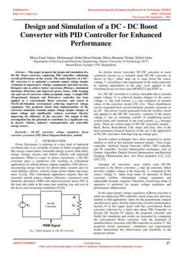
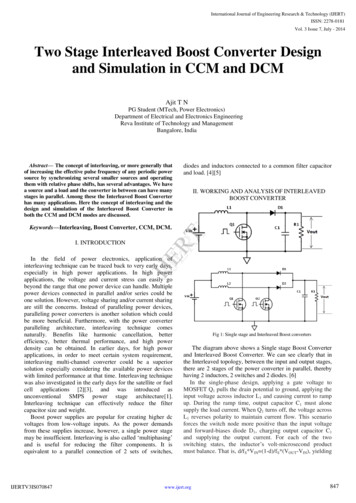
Design Note DN 2013-10V1.0 January 2013CrCM PFC Boost Converter DesignBoost Key WaveformsDC BusPFCConverterACVacDC/DCConverterLoadFigure 2.13PFC Modes of OperationThe boost converter can operate in three modes; continuous conduction mode (CCM), discontinuousconduction mode (DCM), and critical conduction mode (CrCM). Fig. 3.1 shows modeled waveforms toillustrate the inductor and input currents in the three operating modes, for the same exact voltage and powerconditions.15151010Iin ( t)15Iin( t)I in( t)IL ( t)I L ( t)50500-4-4-4-4Continuous Conduction Mode (CCM)1 102 3 10t104 1010IL ( t)50-41 10-4-42 103 10-44 10Critical Conduction Mode (CrM)tFigure 3.1Quick comparison between operting modes is given in the table below:500-41 10-42 10-43 10-44 10Discontinuous ConductionMode (DCM)t
Design Note DN 2013-10V1.0 January 2013CrCM PFC Boost Converter DesignPart /CharacteristicInput CurrentCrCM Variable FrequencyHigh Ripple current - largeEMI filter2High conduction loss: 9-12%I XR MOSFET loss penaltyVariable Frequency CCMLower Ripple Currentsmaller EMILower Ripple Current smaller EMITrapezoidal waveformlower lossTrapezoidal waveformlower lossMOSFET tONQuasi resonant Ton possibleHigh- dependent on BoostdiodeHigh- dependent onboost diodeMOSFET tOFFToff at 2x input current- highlossHigh fSW higher lossesLower - Toff dependent ondesignLower- Toff dependenton designBoost DiodeSlow, cheap type OK- selectfor QRBest performance with SiCor GaNBest performance withSiC or GaNDesign for high ripple- gappedsoft ferrite usually best choice;combine with Litz wire; lowertemp rangeDesign for high average LFcurrent and lower ripplecurrent; powdered core:Kool Mu, High FluxDesign for high averageLF current and lowerripple current; powderedcore: Kool Mu, High FluxSized for fAC input current,very HF RMS ripple currentSized for fAC input current,HF RMS ripple currentSized for fAC inputcurrent, HF RMS ripplecurrentPF/DistortionController and designdependent; can be quite goodController and designdependent; fixed CCMinherently higher distortiondue to current loopController and designdependent; very lowdistortion possible; fewoff the shelf controllersolutionsPower DensityDesign dependent on inductorand semiconductorsDesign dependent oninductor andsemiconductorsDesign dependent oninductor andsemiconductorsLow for lower power levels;EMI filter a limitBetter at higher powerlevelsBetter at higher powerlevelsInductorOutput CapacitorCost4Fixed Frequency CCMCrCM PFC Boost Design EquationsThe following are design equations for the CrCM operated boost, also a design example is integrated tofurther clarify the usage of all equations. The boost converter encounters the maximum current stress and6
Design Note DN 2013-10V1.0 January 2013CrCM PFC Boost Converter Designpower losses at the minimum line voltage condition (will be using the low line voltage condition.), hence, all design equations and power lossesTable 1 SpecificationsInput voltage90-270 Vac 60 HzOutput voltage420 VMaximum power150 WMinimum frequency25 kHzOutput voltage ripple10 Vp-pHold-up time16.6 ms @ Vo.min 350 VEstimated efficiency η0.94.1 Rectifier BridgeThe bridge total power loss is calculated using the average input current flowing through two of the bridgerectifying diodes.4.2 Input CapacitorThe input high frequency filter Cin has to attenuate the switching noise due to the high frequency inductorcurrent ripple (twice of average line current). The worst conditions will occur on the peak of the minimuminput voltage.The maximum high frequency voltage ripple is usually imposed between 1% and 10% of the minimum ratedinput voltage. This is expresses by a coefficient r (typically, r 0.01 to 0.1).High values of Cin helps EMI filter but causes lower power factor to decrease (higher displacemetcomponent), especially at high input voltage and low load. Low values of Cin improve power factor (lowerdisplacement component) but require larger EMI filter.4.3 Input InductorLets define following parameters:a - ratio between peak input voltage and output voltage (DC bus voltage)a max 1.41 VinmaxVo-1a max 9.064 10a min 1.41 VinminVo- 1 load (resistance)Ro- equivalentoutputa min 3.021 107
Design Note DN 2013-10V1.0 January 2013CrCM PFC Boost Converter Design2Ro VoPinRo 1.058 103Switching frequency is changing with input voltage amplitude and angle. Amplitude varies from minimum(90V*1.41 ) to maximum (270*1.41) value. Angle is changing from o to π during each half grid cycle.Switching frequency as function of these two variable is represented on graph below:f ( x y) 1 1 2 y ( 1 - y sin( x) )2 2normalized operating frequencyOne can notice that during each cycle (angle axis) switchingfrequency start with maximum value travels through minimumvalue at peak voltage (angle π/2) and goes back tomaximum. See details below:foperating frequency versus line voltage angle0.25f ( x a max )f x 0.5 0.20.15f ( x a min) 0.10.0500123xAlso, when amplitudechanges from minimum value (90*1.41) to the maximum value (270*1.41) frequency travel from oneminimum through maximum to another minimum value. One needs to choose smaller of these two and useto calculate inductance value. Details are given below:8
Design Note DN 2013-10V1.0 January 2013CrCM PFC Boost Converter Designoperating frequency versus peak input voltage0.04f 2 y 0.030.020.010.4 -2f a max 1.922 10 2 a min 1.593 10- 2 2 f 0.6y0.8Frequency multiplier atmax input voltage.Frequency multiplier at max input voltageOne needs to select condiotion at overall minimum frequency, so:boost inductor value is:Lin Ro min f a min f a max fswmin 2 2 -4Lin 6.743 109
Design Note DN 2013-10V1.0 January 2013CrCM PFC Boost Converter DesignDesign criteria comment:Calculated LP was to obtain operating frequencies higher than 25 kHz at peak input voltage (min or max)and twice of nominal output power (to cover start up and load transients).Let’s calculate other inductor parameters like peak current and RMS current. Peak current is responsible forinductor saturation and RMS current together with inductor resistance produces heat. These threeparameters (Lin, IPKin and IRMSin) determine inductor and a vendor can design and provide inductor basedon them.Peak Input currentPinIPKin 4 a minVo IPKin 5.253RMS Input currentIRMSin IPKin3 2IRMSin 2.1454.4 MOSFETIn order to select the the optimum MOSFET, one must understand the MOSFET requirements in a CrCMboost converter. High voltage MOSFETS have several families based on different technologies, which eachtarget a specific application, topology or operation. For a boost converter, the following are some majorMOSFET selection considerations: Low FOMs - Ron*Qg and Ron*Qoss Fast Turn-on/off switching, gate plateau near middle of gate drive range Low Output capacitance Coss for low switching energy, to increase light load efficiency. Switching and conduction losses must be balancedfor minimum total loss- this is typically optimized atthe low line condition, where worse case lossesand temperature rise occur. VDS rating to handle spikes/overshoots Low thermal resistance RthJC. Package selection must consider the resulting totalthermal resistance from junction to ambient. Body diode speed and reverse recovery charge arenot important, since body diode never conducts in aboost converter.Fig 4.1 Gate voltage versus chargeThe recommended CoolMOS MOSFET series for boostapplications are the CP series and the C6/E6 series.CP CoolMOS provides fastest switching (Error!Reference source not found.), hence, bestperformance, but requires careful design in terms ofgate driving circuit and PCB layout. While C6/E6 seriesprovides cost advantage, easier design, but less performance compare to CP series.MOSFET IPW60R199CP is selected, and its parameters will be used for the following calculations.The MOSFET rms current across the 60Hz line cycle can be calculated by the following equation, andconsequently the MOSFET conduction loss is obtained.10
Design Note DN 2013-10V1.0 January 2013CrCM PFC Boost Converter DesignMOSFET RMS current:RMSsw 1 4 a min69 RMSsw 0.352IRMSsw IPKinRMSsw MOSFET conduction losses are:IRMSsw 1.849The switching losses ,due to current – voltage cross,Conduction Mode operation.occur only at turn-off because of the CriticalAverage input peak current is:Whereis crossover time at turn off. Estimate value is around.Average switching frequency needs to be calculated at minimum input voltage as well.Let’s first calculate MOSFET on time.MOSFET on time at minimum input voltage:IPKin LinT on a minVo -5Ton 2.791 10Switching43.5 1043 1042.5 1042 104frequency fsw ( x)as function of input voltageangle is given on Fig 4.2:fsw ( x) 4 101 ( 1 - a minsin ( x) )T on0123xFig 4.2 Switching frequency as function of angleThe average switching frequency is: fswav 1 fsw ( x) dx 0fswav 2.893 104Now, one can calculate switching losses as:Turn-on the losses are due to the discharge of the total drain-source capacitance inside the MOSFET.Whereis energy contained in the MOSFET output capacitance.11
Design Note DN 2013-10V1.0 January 2013CrCM PFC Boost Converter DesignThis is the worst case scenario, if MOSFET turns on at max voltage. Because MOSFET operates in QRmodeThis value is much smaller, an estimate says that is usually half of this value. So,MOSFET total losses are:4.5 Boost DiodeThe boost freewheeling diode will be a fast recovery one. The value of its DC and RMS current, useful forlosses computation, are respectively:Diode RMS current:RMSd 1 4 a 3 RMSd 0.207IRMSd IPKinRMSd IRMSd 1.086The conduction losses can be estimated as follows:Where(threshold voltage) and Rd (differential resistance) are parameters of the diode.The breakdown voltage is fixed with the same criteria as the MOSFET.4.6 Output Capacitor:The output bulk capacitor (Co) selection depends on the DC output voltage, the output power and thedesired voltage ripple.The 100 to 120Hz (twice the mains frequency) voltage ripple is a function of thecapacitor impedance and the peak capacitor current :Output capacitor value based on ripple:Cor Po4 fl Vo VoCor 2.707 10-5is usually selected in the range of less than 5% of the outputvoltage.Although ESR usually does not affect the output ripple, it has to be taken into account for power lossescalculation. The total RMS capacitor ripple current, including mains frequency and switching frequencycomponents, is:Output capacitor RMS current:12
Design Note DN 2013-10V1.0 January 2013CrCM PFC Boost Converter Design Po Vo 2IRMSd - IRMSc 2IRMSc 1.026If the application has to guarantee a specified hold-up time, the selection criterion of the capacitance willchange: Co has to deliver the output power for a certain time (tHold) with a specified maximum dropoutvoltage:Output capacitor based on hold up time:Coh 2 Po thold22Vo - VominCoh 2.268 10-5where Vomin is the minimum output voltage value (which takes loadregulation and output ripple into (account) and Vopmin is the minimum output operating voltage before the’power fail’ detection from the downstream system supplied by the PFC.Final selection is larger out of these two:Co max(Cor Coh)Co 2.707 10-54.7 HeatsinkThe MOSFET and diode can have separate heatsinks or share the same one, however, the selection of theheatsink is based on its required thermal resistivity.In case of separate heatsinks for the diode andMOSFET, thermal resistors are modeled as in Figure4.1.PFETTJ.FET RthJC.FET TC.FETPdiodeTJ.diodeRthJC.diode TC.diode RthCS.deiode TS.diodeRthSA.diodeRthCS.FET TS.FET RthSA.FETFigure 4.1In case of a single heatsink for both the diode and theMOSFET, thermal resistors are modeled as in Figure4.2.The maximum heatsink temperatureoutcome of the two equations belowis the minimumPFETTJ.FET RthJC.FET TC.FETRthCS.FETTSPdiodeTJ.diodeRthJC.diodeTC.diode RthCS.diodeFigure 4.2Onceis specified, then the heatsink thermalresistance can be calculated.13RthSAPFET PdiodeTA
Design Note DN 2013-10V1.0 January 2013CrCM PFC Boost Converter Designis the thermal resistance from junction to case, this is specified in the MOSFET and Diode datasheets.is the thermal resistace from case to heatsink, typically low compared to the overall thermal resistance,its value depends on the the interface material, for example, thermal grease and thermal pad.is the thermal resistance from heatsink to ambient, this is specified in the heatsink datasheets, itdepends on the heatsink size and design, and is a function of the surroundings, for example, a heatsinkcould have difference values forfor different airflow conditions.is the heatsink temperature,is the case temperature ,is the ambient temperature.is FET’s total power loss ,is diode’s total power loss.14
Design Note DN 2013-10V1.0 January 2013CrCM PFC Boost Converter Design5References[1] CoolMOS Selection Guide.http://www.infineon.com/dgdl/infineon CoolMOS SelectionGuide.pdf?folderId db3a304314dca389011528372fbb12ac&fileId db3a30432f91014f012f95fc7c24399d[2] Infineon Technologies Application Note: “CoolMOS CP - How to make most beneficial use of thelatest generation of super junction technology devices”. February 2007.http://www.infineon.com/dgdl/Aplication Note CoolMOS CP ( AN CoolMOS CP 01 Rev. 1.2).pdf?folderId db3a304412b407950112b408e8c90004&fileId db3a304412b407950112b40ac9a40688[3] Infineon Technologies Application Note: “AN-PFC-TDA4862-1” Octobar l.html?channel ff80808112ab681d0112ab6a73f6050c&tab 2[4] ST Application Note: “AN-966 Enhanced transition mode power factor controller”[5] Infineon Technologies Application Note: “CCM Boost converter design” by Abdel-Rahman Sam,Infineon Technologies; January 2013[6] “PFC topologies and control fundamentals” by Jon Hancock and Mladen Ivankovic, Infineontechnologies Detroit PFC training; September 2011.15
Design Note DN 2013-10V1.0 January 2013CrCM PFC Boost Converter DesignSymbols used in formulasVinmin: Minimum input voltageVo: Output voltageVinmax: Maxmum input voltageVo: Output voltagePo: Output powerfsw: Switching frequencyTsw: Switching time periodfline: line frequencyLin: Input InductorIAVin: Inductor average current across the line cycleIPKin: Inductor peak currentVf.bridge: Bridge diode forward voltage dropPbridge: Bridge power lossoRon(100C): MOSFET on resistance at 100 CQgs: MOSFET gate-source chargeQgd: MOSFET gate-drain chargeQg: MOSFET total gate chargeRg: MOSFET gate resistanceVpl: MOSFET gate plateau voltageVth: MOSFET gate threshold voltageton: MOSFET switching on timetoff: MOSFET switching off timeEoss: MOSFET output capacitance switching energyIRMSsw: MOSFET rms current across the line cyclePcond: MOSFET conduction lossPcross: MOSFET switching off power lossPcap: MOSFET output capacitance switching lossIDo: Boost diode average currentIRMSd: Boost diode average currentVto: Boost diode threshold forward voltage dropPDon: Boost diode conduction lossCo: Output capacitorESR: Output capacitor resistancethold: Hold-up timeVomin: Hold up minimum output voltage Vo: Output voltage rippleIRMSC: Output capacitor rms current16
Critical Conduction Mode (CrM) 0 1u10 4 2u10 4 3u10 4 4u10 4 0 5 10 15 I in ( t) I L ( t) t . further clarify the usage of all equations. The boost converter encounters the maximum current stress and . CrCM PFC Boost Converter Design 7 Design Note DN 2013-10 V1.0 January 2013