Transcription
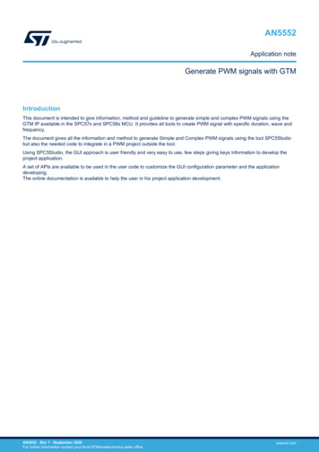
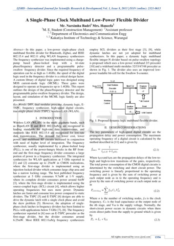
IJSRD - International Journal for Scientific Research & Development Vol. 1, Issue 8, 2013 ISSN (online): 2321-0613A Single-Phase Clock Multiband Low-Power Flexible DividerMr. Narsimha Badri1 Mrs. Haneefa2M. E. Student (Construction Management) 2Assistant professor1, 2Department of Electronics and Communication Engg1, 2Kakatiya Institute of Technology & Science, Warangal1Abstract—In this paper, a low-power single-phase clockmultiband flexible divider for Bluetooth, Zigbee, and IEEE802.15.4 and 802.11 a/b/g WLAN frequency synthesizersThe frequency synthesizer was implemented using a chargepump based phase-locked loop with a tri-statephase/frequency detector and a programmable pulseswallow frequency divider. Since the required frequency ofoperation can be as high as 1.4GHz, the speed of the digitallogic used in the frequency divider is a critical design factor.A custom library of digital logic gates was designed usingMOS current-mode logic (MCML). These gates weredesigned to operate at frequencies up to 1.4GHz. This reportoutlines the design of the phase/frequency detector and theprogrammable pulse-swallow frequency divider. The design,layout, and simulation of the MCML logic family are alsopresented.employ SCL dividers as their first stage [3], [9], whiledynamic latches are not yet adopted for multibandsynthesizers. In this paper, a dynamic logic multibandflexible integer-N divider based on pulse-swallow topologyis proposed which uses a low-power wideband 2/3 prescaler[10] and a wideband multi-modulus 32/33/47/48 prescaler asshown in Fig. 1. The divider also uses an improved lowpower loadable bit-cell for the Swallow S-counter.Key Words: DFF, dual modulus prescaler, dynamic logic, ETSPC, frequency synthesizer, high-speed digital circuits,true single-phase clock (TSPC), wireless LAN (WLAN).I. INTRODUCTIONWireless LAN (WLAN) in the multi gigahertz bands, suchas HiperLAN II and IEEE 802.11a/b/g, are recognized asleading standards for high-rate data transmissions, andstandards like IEEE 802.15.4 are recognized for low-ratedata transmissions. The demand for lower cost, lowerpower, and multiband RF circuits increased in conjunctionwith need of higher level of integration. The frequencysynthesizer, usually implemented by a phase-locked loop(PLL), is one of the power-hungry blocks in the RF frontend and the first-stage frequency divider consumes a largeportion of power in a frequency synthesizer. The integratedsynthesizers for WLAN applications at 5 GHz reported in[1] and [2] consume up to 25mW in CMOS realizations,where the first-stage divider is implemented using aninjection-locked divider which consumes large chip area andhas a narrow locking range. The best published frequencysynthesizer at 5 GHz consumes 9.7mW at 1-V supply,where its complete divider consumes power around 6mW[3], where the first-stage divider is implemented using thesource-coupled logic (SCL) circuit [4], which allows higheroperating frequencies but uses more power. Dynamiclatches are faster and consume less power compared to staticdividers. The TSPC [5] and E-TSPC [6] designs are able todrive the dynamic latch with a single clock phase and avoidthe skew problem [5]. However, the adoption of singlephase clock latches in frequency dividers has been limited toPLLs with applications below 5 GHz [7], [8]. The frequencysynthesizer reported in [6] uses an E-TSPC prescaler as thefirst-stage divider, but the divider consumes around6.25mW. Most IEEE 802.11a/b/g frequency synthesizersFig. 1: Proposed dynamic logic multiband flexible divider.II. DESIGN CONSIDERATIONSThe key parameters of high-speed digital circuits are thepropagation delay and power consumption. The maximumoperating frequency of a digital circuit is calculated by themethod described in [11] and is given by(2.1)Where tpLH and tpHL are the propagation delays of the low-tohigh and high-to-low transitions of the gates, respectively.The total power consumption of the CMOS digital circuits isdetermined by the switching and short circuit power. Theswitching power is linearly proportional to the operatingfrequency and is given by the sum of switching power ateach output node as in to the operating frequency and isgiven by the sum of switching power at each output node asin(2.2)Where n is the number of switching nodes, fclk is the clockfrequency, CLi is the load capacitance at the output node ofthe ith stage, and Vdd is the supply voltage. Normally, theshort-circuit power occurs in dynamic circuits when thereexists direct paths from the supply to ground which is givenby(2.3)All rights reserved by www.ijsrd.com1556
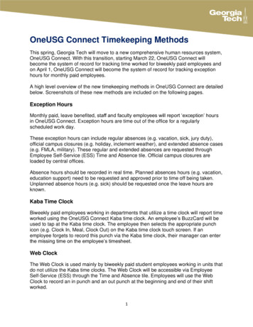
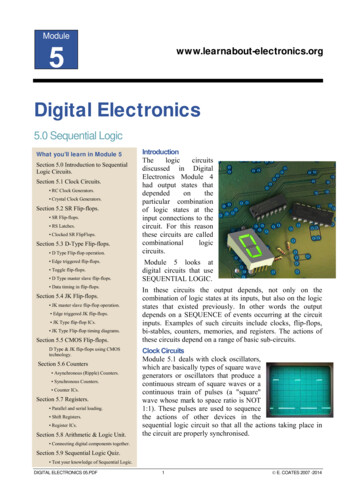
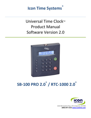
A Single-Phase Clock Multiband Low-Power Flexible Divider(IJSRD/Vol. 1/Issue 8/2013/0008)Where Isc is the short-circuit current. The analysis in [12]shows that the short-circuit power is much higher in ETSPC logic circuits than in TSPC logic circuits. However,TSPC logic circuits exhibit higher switching powercompared to that of E-TSPC logic circuits due to high loadcapacitance. For the E-TSPC logic circuit, the short-circuitpower is the major problem. The E-TSPC circuit has themerit of higher operating frequency than that of the TSPCcircuit due to the reduction in load capacitance, but itconsumes significantly more power than the TSPC circuitdoes for a given transistor size. The following analysis isbased on the latest design using the popular and low-cost0.18-m CMOS process.III. WIDEBAND E-TSPC 2/3 PRESCALERThe dual-modulus prescaler (DMP) divides the VCOfrequency by either N, or N 1, depending on the value ofmodulus control. In this project, N was chosen to be 15 andthe circuit was designed to divide by 16 when moduluscontrol is low and by 15 when modulus control is high. TheDMP was designed as a finite state machine with 16possible states. Four flip-flops were required to generate the16 states, and next-state generation logic was used to cyclethrough the states on each cycle of the input signal from theVCO. The implementation of the DMP is provided in fig. 2.When the modulus control signal is low, all 16 states arepossible; however, setting modulus control high causes thecircuit to skip the zero state. Since only 15 states are used,the DMP divides by15 when the modulus control signal ishigh. The use of the differential MCML logic gates isevident.IV. MULTI MODULUS32/33/47/48 PRESCALERThe proposed wideband multimodulus prescaler which candivide the input frequency by 32, 33, 47, and 48 is shown inFig. 4. It is similar to the 32/33 prescaler used in [7], butwith an additional inverter and a multiplexer. The proposedprescaler performs additional divisions (di-vide-by-47 anddivide-by-48) without any extra flip-flop, thus saving aconsiderable amount of power and also reducing thecomplexity of multiband divider which will be discussed inSection V. The multimodulus prescaler consists of thewideband 2/3(N1/N1 1) prescaler [10], four asynchronousTSPC divide-by-2 circuits ((AD) 16) and combinationallogic circuits to achieve multiple division ratios. Besides theusual Signal for controlling (N1/N1 1) divisions, theadditional control signal Sel is used to switch the prescalerbetween 32/33 and 47/48 modes.Fig. 4: Proposed multimodulus 32/33/47/48 Prescaler.A. Case 1: Sel ’0'When Sel ’0', the output from the NAND2 gate is directlytransferred to the input of 2/3 prescaler and themultimodulus prescaler operates as the normal 32/33prescaler, where the division ratio is controlled by the logicsignal. If MC 1, the 2/3 prescaler operates in the divide-by2 mode and when MC 0, the 2/3 prescaler operates in thedivide-by-3 mode. If MOD 1, the NAND2 gate outputswitches to logic “1” (MC 1) and the wideband prescaleroperates in the di-vide-by-2 mode for entire operation. Thedivision ratio N performed by the multimodulus prescaler is(Fig. 2: Implementation of a 15/16 Dual-Modulus PrescalerIn addition, the three-input OR gate indicated in Figure 2was implemented using 2 two-input OR gates. Figure 3provides the simulation results for the DMP with moduluscontrol set to logic ‘0’. As expected, the frequency of SlowCLK is equal to the input frequency divided by 16. Theseresults suggest that the dual-modulus prescaler operates asdesigned and intended.Fig. 3: Simulation Results for the Dual Modulus Prescaler(Modulus Control 0))(())(3.1)Where N1 2 and AD 16 is fixed for the entire design. If,for 30 input clock cycles MC remains at logic “1”, wherewideband prescaler operates in divide-by-2 mode and, forthree input clock cycles, MC remains at logic “0” where thewideband prescaler operates in the divide-by-3 mode. Thedivision ratio N 1 performed by the multimodulus prescaleris(())(())(3.2)B. Case 2: Sel 1When Sel 1, the inverted output of the NAND2 gate isdirectly transferred to the input of 2/3 prescaler and themultimodulus prescaler operates as a 47/48 prescaler, wherethe division ratio is controlled by the logic signal MOD. IfMC 1, the 2/3 prescaler operates in divide-by-3 mode andwhen MC 0, the 2/3 prescaler operates in divide-by-2 modewhich is quite opposite to the operation performed whenSel ’0' . If MOD 1, the division ratio N 1 performed by themultimodulus prescaler is same as (4) except that the wideband prescaler operates in the divide-by-3 mode for theentire operation given byAll rights reserved by www.ijsrd.com1557
A Single-Phase Clock Multiband Low-Power Flexible Divider(IJSRD/Vol. 1/Issue 8/2013/0008)((())(())(3.2)If MOD 1, the division ratio N performed by themultimodulus prescaler is(() ())()in the equation DIV NP S, the control signal must be setto P-1, since the zero-state is included in the count.(3.3)V. MULTIBANDFLEXIBLEDIVIDERThe single-phase clock multiband flexible divider which isshown in Fig. 1 consists of the multimodulus 32/33/47/48prescaler, a 7-bit programmable S-counter and a 6-bitswallow P-counter. The multi modulus 32/33/47/48prescaler is briefly discussed in Section IV. The controlsignal Sel decides whether the divider is operating in lowerfrequency band (2.4 GHz) or higher band (5–5.825 GHz).A. Program CounterThe program counter is responsible for counting P pulses ofSlow CLK before outputting a pulse to the phase/frequencydetector and reset-ting itself and the swallow counter. Theimplementation used in this project, using a 7-bit ripplecounter, a 7-bit comparator, and a zero-detector is shown inFigure 12. The ripple counter is clocked by Slow CLK, andincrements its count by one each clock cycle. At each stage,the 7-bit comparator compares each count bit to thecorresponding bit in the control signal, and outputs a 0 foreach equal bit. When the zero-detector detects equivalencein all of the 7 bits, indicating that the desired count has beenreached, F out is driven high. On the next clock cycle, theprogram counter is reset to zero and the count is re-started.In addition, the output pulse on F out is used to reset thecount of the swallow counter, indicating the end of onecomplete cycle of the frequency divider. The ripple counteris implemented using 7 cascaded D-type flip-flops, eacharranged in a toggle configuration. The output of each flipflop is used to clock the next flip-flop. Since the output ofeach flip-flop inverts on every clock cycle, each flip- flopessentially divides its clock by two, causing the next stage ofthe ripple counter to be clocked at half the rate of theprevious flip flop. Each flip-flop was designed to respond tothe falling edge of its clock, when the output of theFig. 6: Program Counter Simulation ResultsB. Swallow CounterThe swallow counter, as indicated in Figure 1, is used tocount S pulses of Slow CLK before asserting the moduluscontrol signal and changing the modulus of the DMP to N.A block diagram of the swallow counter is provided inFigure 7.Fig. 7: Block Diagram of a 6-Bit Swallow CounterFig. 5: Block Diagram of a 7-bit Program CounterPrevious stage changes from a 1 to a 0. In this way, anincrementing binary count is achieved with the outputs ofeach flip-flop forming the bits of the count. Since theprogram counter contains 7-bits, any count between 0 and127 can be set by the control signal. It is important to realizehowever that in order to achieve a division ratio as specifiedBy looking at Figure 7, the similarities between the swallowcounter and the program counter are apparent. Once again,the count (6-bits in this case) is maintained using a ripplecounter comprised of cascaded flip-flops clocked with SlowCLK. In addition, a comparator compares each count bitwith its corresponding bit in the control signal, and a zerodetector asserts modulus control when all bits are equal.However, the swallow counter does not reset when the countis reached, but masks the input clock using an AND gateconnected to the inverse of modulus control. As a result, theripple counter stops counting when the count is reached, andthe state of the circuit is maintained until a reset signal(Swallow RST) is received from the program counter. Sincethe swallow counter contains 6 bits, it is capable of anycount from 0 to 64. Once again, the control signal must beset to S-1, since the zero-state is included in the count.All rights reserved by www.ijsrd.com1558
A Single-Phase Clock Multiband Low-Power Flexible Divider(IJSRD/Vol. 1/Issue 8/2013/0008)(2.4–2.484 GHz) and for the higher frequency band (5–5.825 GHz), where K is integer from 1 to 5 for 2.4-GHzband and 5, 10, and 20 for WLAN applications. Table 1shows the performance of different dividers.Fig. 8: Swallow Counter Simulation Results (S 20)VI. SIMULATIONSThe simulations of the designs are performed usingMOIDELSIM 6.4b. The simulation results show that thewide band 2/3 prescaler has the maximum operatingfrequency of 8 GHz with a power consumption of 0.92 and1.73mW during the divide-by-2 and divide-by-3 modes,respectively. The pro-posed wide band multimodulusprescaler has the maximum operating frequency of 7.2 GHz(simulation) with power consumption of 1.52, 1.60, 2.10,and 2.13mW during the divide-by-32, divide-by-33, divideby-47 and divide-by-48, respectively. For siliconverification, the multiband divider is fabricated using theGlobal Foundries 1P6M 0.18-µm CMOS process On-wafermeasurements are carried out using an 8 inch RF probestation. The input signal for the measurement is provided bythe 83650B 10 MHz-50 GHz HP signal generator and theoutput signals are captured by the Lecroy Wave master8600A 6G oscilloscope. The measurement results showsthat the wideband 2/3 prescaler has a maximum operatingfrequency of 6.5 GHz [10] and the multimodulus32/33/47/48 prescaler designed using wideband 2/3prescaler has a maximum operating frequency of 6.2 GHz.However, the maximum operating frequency that can beachieved by the multimodulus 32/33/47/48 prescaler islimited by the wideband 2/3 prescaler. Table I shows theperformance of proposed 2/3 prescaler and prescalersreported in [6] and [12] (re simulated). The performance ofthe multiband flexible divider is measured in both the lowerfrequency and higher frequency bands by programming theP - and S -counters. Fig. 9 shows the measured outputwaveform of the multiband divider at an input frequency of2.47 GHz where P, S -counters are programmed to havevalues 77 and 6 respectively (FD 2470) Fig. 10 shows themeasured output waveform of the multiband divider at aninput frequency of 5.818 GHz where P, S -counters areprogrammed to have values 122 and 38, respectively(FD 5818) The proposed multiband flexible dividerconsumes an average power of 0.96mW during lowerfrequency band (2.4–2.484GHz),While it consumes 2.2mW during the high-frequency band(5–5.825 GHz) of operation compared to the dual-banddivider re-ported in [9], which consumes 2.7mW at 1-Vpower supply. The proposed multiband divider has avariable resolution of K MHz for lower frequency bandTable. 1: Performance of different 2/3 Prescalers at 2.5 GHzVII. CONCLUSIONIn this paper, a wideband 2/3 prescaler is verified in thedesign of proposed wide band multimodulus 32/33/47/48prescaler. A dynamic logic multiband flexible integerdivider is designed which uses the wideband 2/3 prescaler[17], multimodulus 32/33/47/48 prescaler, and is siliconverified using the0.18µm CMOS technology. Since themultimodulus 32/33/47/48 prescaler has maximumoperating frequency of 6.2 GHz, the values of P- and Scounters can actually be programmed to divide over thewhole range of frequencies from 1 to 6.2 GHz with finestresolution of 1 MHz and variable channel spacing.However, since interest lies in the 2.4- and 5–5.825-GHzbands of operation, the P- and S-counters are programmedaccordingly. The proposed multiband flexible divider alsouses an improved loadable bit-cell for Swallow S-counterand consumes a power of 0.96 and 2.2mW in 2.4- and 5GHz bands, respectively, and provides a solution to the lowpower PLL synthesizers for Bluetooth, Zigbee, IEEE802.15.4, and IEEE 802.11a/b/g WLAN applications withvariable channel spacing.REFERENCES[1] H. R. Rateghet al., “A CMOS frequency synthesizerwith an injected-locked frequency divider for 5-GHzwireless LAN receiver,” IEEE J. Solid-State Circuits,vol. 35, no. 5, pp. 780–787, May 2000.[2] P. Y. Denget al., “A 5 GHz frequency synthesizer withan injection-locked frequency divider and differentialswitched capacitors,” IEEE Trans. Circuits Syst. I, Reg.Papers, vol. 56, no. 2, pp. 320–326, Feb. 2009.[3] L. Lai Kan Leunget al., “A 1-V 9.7-mW CMOSfrequency synthesizer for IEEE 802.11a transceivers,”IEEE Trans. Microw. Theory Tech., vol. 56, no. 1, pp.39–48, Jan. 2008.[4] M. Alioto and G. Palumbo, Model and Design ofBipolar and MOS Current-Mode Logic Digital Circuits.New York: Springer, 2005.[5] Y. Ji-renet al., “A true single-phase-clock dynamicCMOS circuit tech-nique,”IEEE J. Solid-State Circuits,vol. 24, no. 2, pp. 62–70, Feb. 1989.[6] S. Pellerano et al., “A 13.5-mW 5 GHz der,”IEEE J. Solid-State Circuits, vol. 39, no. 2, pp.378–383, Feb. 2004.All rights reserved by www.ijsrd.com1559
A Single-Phase Clock Multiband Low-Power Flexible Divider(IJSRD/Vol. 1/Issue 8/2013/0008)[7] V. K. Manthenaet al., “A low power fullyprogrammable 1 MHz resolution 2.4 GHz CMOS PLLfrequency synthesizer,” in Proc. IEEE Biomed. CircuitsSyst. Conf., Nov. 2007, pp. 187–190.[8] S. Shinet al., “4.2 mW frequency synthesizer for 2.4GHz ZigBee application with fast settling timeperformance,” in IEEE MTT-S Int. Mi-crow. Symp.Dig., Jun. 2006, pp. 411–414.[9] S. Vikaset al., “1 V 7-mW dual-band fast-lockedfrequency synthesizer,” in Proc. 15th ACM Symp.VLSI, 2005, pp. 431–435.[10] V. K. Manthenaet al., “A 1.8-V 6.5-GHz low powerwide band single-phase clock CMOS 2/3 prescaler,” inIEEE 53rd Midwest Symp. Circuits Syst., Aug. 2010,pp. 149–152.[11] J. M. Rabaey al., “Digital integrated circuits, a designperspective,” in Ser. Electron and VLSI, 2nd ed. UpperSaddle River, NJ: Prentice-Hall, 2003.[12] X. P. Yet al., “Design and optimization of the extendedtrue single-phase clock-based prescaler,” IEEE Trans.Microw. Theory Tech., vol. 56, no. 11, pp. 3828–3835,Nov. 2006.[13] X. P. Yuet al., “Design of a low power wideband highresolution programmable frequency divider,”IEEETrans. Very Large Scale Integration. (VLSI) Syst., vol.13, no. 9, pp. 1098–1103, Sep. 2005All rights reserved by www.ijsrd.com1560
flexible integer-N divider based on pulse-swallow topology is proposed which uses a low-power wideband 2/3 prescaler [10] and a wideband multi-modulus 32/33/47/48 prescaler as shown in Fig. 1. The divider also uses an improved low-power loadable bit-cell for the Swallow S-counter. Fig. 1: Proposed dynamic logic multiband flexible divider. II.