Transcription
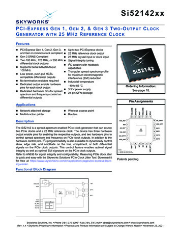
Si52142PCI-E XPRESS G EN 1, G EN 2, & G EN 3 TW O O UTPUTC L O C K G ENERATOR WITH 2 5 M H Z R E F E R E N C E C L O C KFeatures PCI-Express Gen 1, Gen 2, Gen 3, and Gen 4 common clock compliant Gen 3 SRNS Compliant Two 100 MHz, 125 MHz, or 200 MHz differential clock outputs Supports Serial ATA (SATA) at100 MHz Low power, push-pull HCSLcompatible differential outputsNo termination resistors required Dedicated output enable hardwarepins for each clock output Dedicated hardware pins for spread spectrum and frequency control ondifferential outputsUp to two PCI-Express clocks25 MHz reference clock output25 MHz crystal input or clock inputSignal integrity tuningI2C support with readbackcapabilitiesTriangular spread spectrum profilefor maximum electromagneticinterference (EMI) reductionIndustrial temperature–40 to 85 oC3.3 V power supply24-pin QFN packageOrdering Information:See page 18.VDD CORESCLK22SDATA232120191118 OE DIFF1REF217 VDD DIFFOE REF3VSS REF4OE DIFF015VDD DIFF616 DIFF125GND15 DIFF114 DIFF013 DIFF0789101112VDD DIFF1The Si52142 is a spread-spectrum enabled PCIe clock generator that can sourcetwo PCIe clocks and a 25 MHz reference clock. The device has three hardwareoutput enable pins for enabling the respective outputs, and two hardware pins tocontrol spread spectrum and frequency on PCIe clock outputs. In addition to thehardware control pins, I2C programmability is also available to dynamically controlskew, edge rate, and amplitude on the true, compliment, or both differentialsignals on the PCIe clock outputs. This control feature enables optimal signalintegrity as well as optimal EMI signature on the PCIe clock outputs.Refer to AN636 for signal integrity and configurability. Measuring PCIe clock jitteris quick and easy with the Silicon Labs PCIe Clock Jitter Tool. Download it for freeat www.silabs.com/pcie-learningcenter.24VDD REFNCDescriptionXOUTWireless access pointRoutersNC NC Network attached storageMulti-function printerSS12 SS02 XIN/CLKINApplicationsVSS COREPin AssignmentsNotes:1. Internal 100 kohm pull-up.2. Internal 100 kohm pull-down.Patents pendingFunctional Block CLKSDATAControl & MemoryOE REFOE [1:0]ControlRAMSS [1:0]Rev 1.3 12/15Copyright 2015 by Silicon LaboratoriesSi52142
Si521422Rev 1.3
Si52142TABLE O F C ONTENTSSectionPage1. Electrical Specifications . . . . . . . . . . . . . . . . . . . . . . . . . . . . . . . . . . . . . . . . . . . . . . . . . . . . . . . . . 42. Functional Description . . . . . . . . . . . . . . . . . . . . . . . . . . . . . . . . . . . . . . . . . . . . . . . . . . . . . . . . . . . 72.1. Crystal Recommendations . . . . . . . . . . . . . . . . . . . . . . . . . . . . . . . . . . . . . . . . . . . . . . . . . . . 72.2. OE Pin Definition . . . . . . . . . . . . . . . . . . . . . . . . . . . . . . . . . . . . . . . . . . . . . . . . . . . . . . . . . . . 82.3. OE Assertion . . . . . . . . . . . . . . . . . . . . . . . . . . . . . . . . . . . . . . . . . . . . . . . . . . . . . . . . . . . . . . 82.4. OE Deassertion . . . . . . . . . . . . . . . . . . . . . . . . . . . . . . . . . . . . . . . . . . . . . . . . . . . . . . . . . . . . 82.5. SS[1:0] Pin Definition . . . . . . . . . . . . . . . . . . . . . . . . . . . . . . . . . . . . . . . . . . . . . . . . . . . . . . . 83. Test and Measurement Setup . . . . . . . . . . . . . . . . . . . . . . . . . . . . . . . . . . . . . . . . . . . . . . . . . . . . . 94. Control Registers . . . . . . . . . . . . . . . . . . . . . . . . . . . . . . . . . . . . . . . . . . . . . . . . . . . . . . . . . . . . . . 114.1. I2C Interface . . . . . . . . . . . . . . . . . . . . . . . . . . . . . . . . . . . . . . . . . . . . . . . . . . . . . . . . . . . . . 114.2. Data Protocol . . . . . . . . . . . . . . . . . . . . . . . . . . . . . . . . . . . . . . . . . . . . . . . . . . . . . . . . . . . . 115. Pin Descriptions: 24-Pin QFN . . . . . . . . . . . . . . . . . . . . . . . . . . . . . . . . . . . . . . . . . . . . . . . . . . . . 166. Ordering Guide . . . . . . . . . . . . . . . . . . . . . . . . . . . . . . . . . . . . . . . . . . . . . . . . . . . . . . . . . . . . . . . . 187. Package Outline . . . . . . . . . . . . . . . . . . . . . . . . . . . . . . . . . . . . . . . . . . . . . . . . . . . . . . . . . . . . . . . 19Document Change List . . . . . . . . . . . . . . . . . . . . . . . . . . . . . . . . . . . . . . . . . . . . . . . . . . . . . . . . . . . . 20Rev 1.33
Si521421. Electrical SpecificationsTable 1. DC Electrical SpecificationsParameterSymbolTest ConditionMinTypMaxUnit3.3 V Operating VoltageVDD core3.3 5%3.1353.33.465V3.3 V Input High VoltageVIHControl input pins2.0—VDD 0.3V3.3 V Input Low VoltageVILControl input pinsVSS –0.3—0.8VInput High VoltageVIHI2CSDATA, SCLK2.2——VInput Low VoltageVILI2CSDATA, SCLK——1.0VInput High Leakage CurrentIIHExcept internal pull-downresistors, 0 VIN VDD——5 AInput Low Leakage CurrentIILExcept internal pull-up resistors, 0 VIN VDD–5—— A3.3 V Output High Voltage(Single-Ended Outputs)VOHIOH –1 mA2.4——V3.3 V Output High Voltage(Single-Ended Outputs)VOLIOL 1 mA——0.4VHigh-impedance Output CurrentIOZ–10—10µAInput Pin �—40mAOutput Pin CapacitancePin InductanceDynamic Supply CurrentIDD 3.3VAll outputs enabled. Differential clocks with 5” tracesand 2 pF load.Table 2. AC Electrical SpecificationsParameterSymbolTest ConditionMinTypMaxUnitLACCMeasured at VDD/2 differential——250ppmTDCMeasured at VDD/245—55%CLKIN Rising and Falling SlewRateTR/TFMeasured between 0.2 VDD and0.8 VDD0.5—4.0V/nsCycle to Cycle JitterTCCJMeasured at VDD/2——250psLong Term JitterTLTJMeasured at VDD/2——350psCrystalLong-term AccuracyClock InputDuty CycleNotes:1. Visit www.pcisig.com for complete PCIe specifications.2. Gen 4 specifications based on the PCI-Express Base Specification 4.0 rev. 0.5.3. Download the Silicon Labs PCIe Clock Jitter Tool at www.silabs.com/pcie-learningcenter.4Rev 1.3
Si52142Table 2. AC Electrical Specifications (Continued)ParameterSymbolTest ConditionMinTypMaxUnitInput High VoltageVIHXIN/CLKIN pin2—VDD 0.3VInput Low VoltageVILXIN/CLKIN pin——0.8VInput High CurrentIIHXIN/CLKIN pin, VIN VDD——35µAInput Low CurrentIILXIN/CLKIN pin, 0 VIN 0.8–35——µATDCMeasured at 0 V differential45—55%Output-Output SkewTSKEWMeasured at 0 V differential——50psCycle to Cycle JitterTCCJMeasured at 0 V differential—3550psPCIe Gen 1 Pk-Pk Jitter,Common ClockPk-PkPCIe Gen 104045psPCIe Gen 2 Phase Jitter,Common ClockRMSGEN210 kHz F 1.5 MHz01.82.0ps1.5 MHz F Nyquist Rate01.82.0psPCIe Gen 3 Phase Jitter,Common ClockRMSGEN3PLL BW 2–4 MHzCDR 10 MHz00.50.6psPCIe Gen 3 Phase Jitter,Separate Reference NoSpread, SRNSRMSGEN3 SRNSPLL BW of 2–4 or 2–5 MHz,CDR 10 MHz—0.350.42psPCIe Gen 4 Phase Jitter,Common ClockRMSGEN4PLL BW of 2–4 or 2–5 MHz,CDR 10 MHz—0.50.6psLACCMeasured at 0 V differential——100ppmRising/Falling Slew RateT R / TFMeasured differentially from 150 mV1—8V/nsVoltage HighVHIGH——1.15VVoltage LowVLOW–0.3——VCrossing Point Voltage at0.7 V SwingVOX300—550mVSpread RangeSPR—–0.5—%Modulation FrequencyFMOD3031.533kHzDIFF at 0.7 VDuty CycleLong Term AccuracyDown spreadNotes:1. Visit www.pcisig.com for complete PCIe specifications.2. Gen 4 specifications based on the PCI-Express Base Specification 4.0 rev. 0.5.3. Download the Silicon Labs PCIe Clock Jitter Tool at www.silabs.com/pcie-learningcenter.Rev 1.35
Si52142Table 2. AC Electrical Specifications (Continued)ParameterSymbolTest ConditionMinTypMaxUnitTDCMeasurement at 1.5 V45—55%TR / TFMeasured between 0.8 and 2.0 V1.0—4.0V/nsCycle to Cycle JitterTCCJMeasurement at 1.5 V——300psLong Term AccuracyLACCMeasured at 1.5 V——100ppmREF(25 MHz) at 3.3 VDuty CycleRising and Falling Edge RateEnable/Disable and Set-UpClock Stabilization fromPower-upTSTABLE——1.8msStopclock Set-up TimeTSS10.0——nsNotes:1. Visit www.pcisig.com for complete PCIe specifications.2. Gen 4 specifications based on the PCI-Express Base Specification 4.0 rev. 0.5.3. Download the Silicon Labs PCIe Clock Jitter Tool at www.silabs.com/pcie-learningcenter.Table 3. Absolute Maximum ConditionsParameterSymbolTest ConditionMinTypMaxUnitVDD 3.3VFunctional——4.6VInput VoltageVINRelative to VSS–0.5—4.6VDCTemperature, StorageTSNon-functional–65—150 CTemperature, Operating AmbientTAFunctional–40—85 CTemperature, JunctionTJFunctional——150 CDissipation, Junction to CaseØJCJEDEC (JESD 51)——35 C/WDissipation, Junction to AmbientØJAJEDEC (JESD 51)——37 C/WESDHBMJEDEC (JESD 22-A114)2000——VUL-94UL (Class)Main Supply VoltageESD Protection (Human Body Model)Flammability RatingV–0Note: While using multiple power supplies, the voltage on any input or I/O pin cannot exceed the power pin during power-up. Powersupply sequencing is not required.6Rev 1.3
Si521422. Functional Description2.1. Crystal RecommendationsIf using crystal input, the device requires a parallel resonance 25 MHz crystal.Table 4. Crystal RecommendationsFrequency(Fund)CutLoading Load Cap25 MHzATParallel12–15 pFShuntCap g(max)5 pF0.016 pF35 ppm30 ppm5 ppm2.1.1. Crystal LoadingCrystal loading is critical for ppm accuracy. In order to achieve low/zero ppm error, use the calculations below insection 2.1.2 to estimate the appropriate capacitive loading (CL).Figure 1 shows a typical crystal configuration using two trim capacitors. It is important that the trim capacitors are inseries with the crystal.Figure 1. Crystal Capacitive Clarification2.1.2. Calculating Load CapacitorsIn addition to the standard external trim capacitors, consider the trace capacitance and pin capacitance to calculatethe crystal loading correctly. The capacitance on each side is in series with the crystal. The total capacitance onboth sides is twice the specified crystal load capacitance (CL). Trim capacitors are calculated to provide equalcapacitive loading on both sides.Figure 2. Crystal Loading ExampleUse the following formulas to calculate the trim capacitor values for Ce1 and Ce2.Rev 1.37
Si52142Load Capacitance (each side)Ce 2 x CL – (Cs Ci)Total Capacitance (as seen by the crystal)CLe 11( Ce1 Cs1 Ci1 1Ce2 Cs2 Ci2) CL:Crystal load capacitance CLe: Actual loading seen by crystal using standard value trim capacitors Ce: External trim capacitors Cs: Stray capacitance (terraced) Ci : Internal capacitance (lead frame, bond wires, etc.)2.2. OE Pin DefinitionThe OE pins are active high inputs used to enable and disable the output clocks. To enable the output clock, the OEpin needs to be logic high and the I2C output enable bit needs to be logic high. There are two methods to disablethe output clocks: the OE is pulled to a logic low, or the I2C enable bit is set to a logic low. The OE pins is requiredto be driven at all time and even though it has an internally 100 k resistor.2.3. OE AssertionThe OE signals are active high input used for synchronous stopping and starting the output clocks respectively whilethe rest of the clock generator continues to function. The assertion of the OE signal by making it logic high causesstopped respective output clocks to resume normal operation. No short or stretched clock pulses are produced whenthe clock resumes. The maximum latency from the assertion to active outputs is no more than two to six output clockcycles.2.4. OE DeassertionWhen the OE pin is deasserted by making its logic low, the corresponding output clocks are stopped cleanly, andthe final output state is driven low.2.5. SS[1:0] Pin DefinitionSS[1:0] are active inputs used to select differential output frequency and enable spread of –0.5% on all DIFFoutputs as per Table 5.Table 5. SS0 and SS1 Frequency/Spread preadConfiguration00100 MHzSpread OffDefault01100 MHz–0.50%10125 MHzSpread Off11200 MHzSpread OffRev 1.3
Si521423. Test and Measurement SetupFigure 3 shows the test load configuration for the HCSL compatible clock outputs.M e a s u re m e n tP o in tL1O UT 50 2 pFL1 5"M e a s u re m e n tP o in tL1O UT-50 2 pFFigure 3. 0.7 V Differential Load ConfigurationPlease reference application note AN781 for recommendations on how to terminate the differential outputs forLVDS, LVPECL, or CML signaling levels.Figure 4. Differential Measurement for Differential Output Signals(for AC Parameters Measurement)Rev 1.39
Si52142VMIN –0.30VVMIN –0.30VFigure 5. Single-ended Measurement for Differential Output Signals(for AC Parameters Measurement)L1 0.5", L2 5"Measurement50 SE ClocksPointL133 L24 pFFigure 6. Single-ended Clocks with Single Load ConfigurationFigure 7. Single-ended Output Signal (for AC Parameter Measurement)10Rev 1.3
Si521424. Control Registers4.1. I2C InterfaceTo enhance the flexibility and function of the clock synthesizer, an I2C interface is provided. Through the I2CInterface, various device functions are available, such as individual clock enablement. The registers associatedwith the I2C Interface initialize to their default setting at power-up. The use of this interface is optional. Clock deviceregister changes are normally made at system initialization, if any are required. Power management functions canonly be programed in program mode and not in normal operation modes.4.2. Data ProtocolThe clock driver I2C protocol accepts byte write, byte read, block write, and block read operations from thecontroller. For block write/read operation, access the bytes in sequential order from lowest to highest (mostsignificant bit first) with the ability to stop after any complete byte is transferred. For byte write and byte readoperations, the system controller can access individually indexed bytes.The block write and block read protocol is outlined in Table 6 while Table 7 outlines byte write and byte readprotocol. The slave receiver address is 11010110 (D6h).Table 6. Block Read and Block Write ProtocolBlock Write ProtocolBit18:2Block Read ProtocolDescriptionBit1Start8:2Slave address—7 bitsDescriptionStartSlave address—7 bits9Write9Write10Acknowledge from slave10Acknowledge from slave18:11Command Code—8 bits18:11Command Code—8 bits19Acknowledge from slave19Acknowledge from slaveByte Count—8 bits20Repeat start27:202836:293745:38Acknowledge from slave27:21Slave address—7 bitsData byte 1—8 bits28Read 1Acknowledge from slave29Acknowledge from slaveData byte 2—8 bits46Acknowledge from slave.Data Byte /Slave Acknowledges.Data Byte N—8 bits.Acknowledge from slave.Stop37:303846:394755:48Rev 1.3Byte Count from slave—8 bitsAcknowledgeData byte 1 from slave—8 bitsAcknowledgeData byte 2 from slave—8 bits56Acknowledge.Data bytes from slave/Acknowledge.Data Byte N from slave–8 bits.NOT Acknowledge.Stop11
Si52142Table 7. Byte Read and Byte Write ProtocolByte Write ProtocolBit18:2Byte Read ProtocolDescriptionBitStart1Slave address–7 bits8:2StartSlave address–7 bits9Write9Write10Acknowledge from slave10Acknowledge from slave18:111927:20Command Code–8 bits18:11Command Code–8 bitsAcknowledge from slave19Acknowledge from slaveData byte–8 bits20Repeated start28Acknowledge from slave29Stop27:21Rev 1.3Slave address–7 bits28Read29Acknowledge from slave37:3012DescriptionData from slave–8 bits38NOT Acknowledge39Stop
Si52142Control Register 0. Byte 0BitD7D6D5D4D3D1D0R/WR/WR/WREF OENameTypeD2R/WR/WR/WR/WR/WReset settings 00000100BitNameFunction7:3Reserved2REF OEOutput Enable for REF.0: Output disabled.1: Output enabled.1:0ReservedControl Register 1. Byte peReset settings 00000000BitName7:0ReservedFunctionRev 1.313
Si52142Control Register 2. Byte 2BitD7D6NameDIFF0 OEDIFF1 set settings 11000000BitName7DIFF0 OEFunctionOutput Enable for DIFF0.0: Output disabled.1: Output enabled.6DIFF1 OEOutput Enable for DIFF1.0: Output disabled.1: Output enabled.5:0ReservedControl Register 3. Byte 3BitD7D6NameTypeD5D4D3Rev Code[3:0]R/WR/WR/WVendor ID[3:0]R/WR/WR/WR/WR/WD3D2D1D0R/WR/WR/WR/WReset settings 00001000BitNameFunction7:4Rev Code[3:0]Program Revision Code.3:0Vendor ID[3:0]Vendor Identification Code.Control Register 4. Byte 4BitD7D6D5D4NameTypeBC[7:0]R/WR/WR/WR/WReset settings 0000011014BitName7:0BC[7:0]FunctionByte Count Register.Rev 1.3
Si52142Control Register 5. Byte 5BitD7D6D5D4D3D2D1D0R/WR/WR/WR/WName DIFF Amp Sel DIFF Amp Cntl[2] DIFF Amp Cntl[1] DIFF Amp Cntl[0]TypeR/WR/WR/WR/WReset settings 11011000BitName7DIFF Amp SelFunctionAmplitude Control for DIFF Differential Outputs.0: Differential outputs with Default amplitude.1: Differential outputs amplitude is set by Byte 5[6:4].6DIFF Amp Cntl[2]5DIFF Amp Cntl[1]4DIFF Amp Cntl[0]3:0ReservedDIFF Differential Outputs Amplitude Adjustment.000: 300 mV 001: 400 mV 010: 500 mV100: 700 mV 101: 800 mV 110: 900 mVRev 1.3011: 600 mV111: 1000 mV15
Si52142VSS COREXIN/CLKINXOUTVDD CORESDATASCLK5. Pin Descriptions: 24-Pin QFN242322212019VDD REF1118 OE DIFF1REF217 VDD DIFFOE REF13VSS REF4OE DIFF015VDD DIFF616 DIFF125GND15 DIFF114 DIFF0789101112SS02SS12NCNCNCVDD DIFF13 DIFF0Notes:1. Internal 100 kohm pull-up.2. Internal 100 kohm pull-down.Table 8. Si52142 24-Pin QFN DescriptionsPin #Name1VDD REF2REF3OE REFI,PUActive high input pin to enable or disable REF clock (internal 100 k pull-up).4VSS REFGNDGround.5OE DIFF0I,PUActive high input pin to enable or disable DIFF0 clock (internal 100 k pull-up).6VDD DIFFPWR 3.3 V power supply.7SS0I, PD8SS1I, PD9NCNCNo Connect.10NCNCNo connect.16TypeDescriptionPWR 3.3 V power supply.O, SE 3.3 V, 25 MHz crystal reference clock output.3.3 V tolerant latch-input for enabling Frequency/ Spread selection onDIFF0 and DIFF1 outputs. Refer to Table 1 on page 4 for SS[1:0] specifications (internal 100 k pull-down).Rev 1.3
Si52142Table 8. Si52142 24-Pin QFN Descriptions (Continued)Pin #NameTypeDescription11NCNC12VDD DIFF13DIFF0O, DIF 0.7 V, 100 MHz differential clock output.14DIFF0O, DIF 0.7 V, 100 MHz differential clock output.15DIFF1O, DIF 0.7 V, 100 MHz differential clock output.16DIFF1O, DIF 0.7 V, 100 MHz differential clock output.17VDD DIFFPWR 3.3 V power supply.18OE DIFF1I,PU19SCLKI20SDATAI/O21VDD CORE22XOUTO25.00 MHz Crystal output, Float XOUT if using only CLKIN (Clock input).23XIN/CLKINI25.00 MHz Crystal input or 3.3 V, 25 MHz Clock Input.24VSS COREGNDGround.25GNDGNDGround for bottom pad of the IC.No connect.PWR 3.3 V power supply.Active high input pin to enable or disable DIFF1 clock (internal 100 k pull-up).I2C SCLOCK.I2C SDATA.PWR 3.3 V power supply.Rev 1.317
Si521426. Ordering GuidePart NumberPackage TypeTemperatureSi52142-A01AGM24-pin QFNIndustrial, –40 to 85 CSi52142-A01AGMR24-pin QFN—Tape and ReelIndustrial, –40 to 85 CLead-free18Rev 1.3
Si521427. Package OutlineFigure 8 illustrates the package details for the Si52142. Table 9 lists the values for the dimensions shown in theillustration.Figure 8. 24-Pin Quad Flat No Lead (QFN) PackageTable 9. Package Diagram 0.000.0250.05b0.200.250.30ADD24.00 BSC2.602.70e0.50 BSCE4.00 c0.08ddd0.07Notes:1. All dimensions shown are in millimeters (mm) unless otherwisenoted.2. Dimensioning and Tolerancing per ANSI Y14.5M-1994.3. This drawing conforms to JEDEC outline MO-220, variation VGGD-8.4. Recommended card reflow profile is per the JEDEC/IPC J-STD-020specification for Small Body Components.Rev 1.319
Si52142DOCUMENT CHANGE LISTRevision 0.1 to Revision 1.0 Updated Features on page 1.Updated Description on page 1.Updated Table 1 on page 4.Updated Table 2 on page 5.Updated Section 2.1 on page 7.Updated Section 2.1.1 on page 7.Updated Section 4.1 on page 11.Updated Section 4.2 on page 11.Updated Pin Descriptions on page 16.Revision 1.0 to Revision 1.1 Removed Moisture Sensitivity Level specificationfrom Table 3.Revision 1.1 to Revision 1.2 Updated Table 2.Updated Section 3.Revision 1.2 to Revision 1.3 Updated Features on page 1. Updated Description on page 1. Updated Table 2, “AC Electrical Specifications,” onpage 4.20Rev 1.3
ClockBuilder ProOne-click access to Timing tools,documentation, software, sourcecode libraries & more. Available forWindows and iOS (CBGo only).www.silabs.com/CBProTiming Portfoliowww.silabs.com/timingSW/HWQualitySupport and ycommunity.silabs.comDisclaimerSilicon Laboratories intends to provide customers with the latest, accurate, and in-depth documentation of all peripherals and modules available for system and software implementersusing or intending to use the Silicon Laboratories products. Characterization data, available modules and peripherals, memory sizes and memory addresses refer to each specificdevice, and "Typical" parameters provided can and do vary in different applications. Application examples described herein are for illustrative purposes only. Silicon Laboratoriesreserves the right to make changes without further notice and limitation to product information, specifications, and descriptions herein, and does not give warranties as to the accuracyor completeness of the included information. Silicon Laboratories shall have no liability for the consequences of use of the information supplied herein. This document does not implyor express copyright licenses granted hereunder to design or fabricate any integrated circuits. The products must not be used within any Life Support System without the specificwritten consent of Silicon Laboratories. A "Life Support System" is any product or system intended to support or sustain life and/or health, which, if it fails, can be reasonably expectedto result in significant personal injury or death. Silicon Laboratories products are generally not intended for military applications. Silicon Laboratories products shall under nocircumstances be used in weapons of mass destruction including (but not limited to) nuclear, biological or chemical weapons, or missiles capable of delivering such weapons.Trademark InformationSilicon Laboratories Inc., Silicon Laboratories, Silicon Labs, SiLabs and the Silicon Labs logo, CMEMS , EFM, EFM32, EFR, Energy Micro, Energy Micro logo and combinationsthereof, "the world’s most energy friendly microcontrollers", Ember , EZLink , EZMac , EZRadio , EZRadioPRO , DSPLL , ISOmodem , Precision32 , ProSLIC , SiPHY ,USBXpress and others are trademarks or registered trademarks of Silicon Laboratories Inc. ARM, CORTEX, Cortex-M3 and THUMB are trademarks or registered trademarks ofARM Holdings. Keil is a registered trademark of ARM Limited. All other products or brand names mentioned herein are trademarks of their respective holders.Silicon Laboratories Inc.400 West Cesar ChavezAustin, TX 78701USAhttp://www.silabs.com
PCI-EXPRESS GEN 1, GEN 2, & GEN 3 TWO OUTPUT CLOCK GENERATOR WITH 25 MHZ REFERENCE CLOCK Features Applications Description The Si52142 is a spread-spectrum enabled PCIe clock generator that can source two PCIe clocks and a 25 MHz reference clock. The device has three hardware output enable pins for enabling the respective outputs, and two .


![PCI Compliant - but are we secure -- FOR PRINTING IN GRAYSCALE [Read-Only]](/img/14/303-pci-3.jpg)