Transcription
AN4758Application noteProprietary code read-out protection onSTM32L4, STM32L4 , STM32G4 and STM32WB Series MCUsIntroductionSoftware providers are developing complex middleware solutions known as IP (intellectualpropriety) code, whose protection is a high importance issue for microcontrollers.To respond to this important requirement, STM32L4, STM32L4 , STM32G4 and STM32WBSeries MCUs are provided with the following protection features: Read-out protection (RDP): protection against read operations Write protection: protection against undesired write or erase operations Proprietary code read-out protection (PCROP): protection against read and writeoperations on Flash and SRAM memories. Firewall: access protection to sensitive code and data against external processes.This application note provides a description of the Flash memory protection features,focusing on the PCROP technique, and providing a basic example of it. Firewall protection(available on STM32L4 and STM32L4 Series) is described in AN4729 “STM32L0/L4FIREWALL overview”, available on www.st.com).The X-CUBE-PCROP firmware package is delivered with this document. It contains thesource code of the PCROP example with all firmware modules required to run the examplebased on STM32L4 Series microcontrollers, and easily portable to STM32L4 , STM32G4and STM32WB Series microcontrollers.This application note must be read in conjunction with product datasheets and the followingreference manuals, available on www.st.com:July 2021 RM0351 (STM32L4x5xx, STM32L4x6xx) RM0392 (STM32L4x1xx) RM0394 (STM32L43xxx, STM32L44xxx, STM32L45xxx, STM32L46xxx) RM0432 (STM32L4Rxxx and STM32L4Sxxx) RM0440 (STM32G4xx) RM0434 (STM32WB55xx and STM32WB35xx) RM0471 (STM32WB50CG and STM32WB30CE) RM0473 (STM32WB15CC) RM0478 (STM32WB10CC)AN4758 Rev 61/43www.st.com1
ContentsAN4758Contents1Memory protection description . . . . . . . . . . . . . . . . . . . . . . . . . . . . . . . . 61.11.21.31.421.1.1Read protection Level 0 . . . . . . . . . . . . . . . . . . . . . . . . . . . . . . . . . . . . . . 61.1.2Read protection Level 1 . . . . . . . . . . . . . . . . . . . . . . . . . . . . . . . . . . . . . . 61.1.3Read protection Level 2 . . . . . . . . . . . . . . . . . . . . . . . . . . . . . . . . . . . . . . 71.1.4Internal Flash memory content updating on an RDP protected STM32 . 7Write protection . . . . . . . . . . . . . . . . . . . . . . . . . . . . . . . . . . . . . . . . . . . . . 81.2.1Flash memory write protection . . . . . . . . . . . . . . . . . . . . . . . . . . . . . . . . . 81.2.2SRAM2 CCM-SRAM write protection . . . . . . . . . . . . . . . . . . . . . . . . . . . 9Proprietary code readout protection (PCROP) . . . . . . . . . . . . . . . . . . . . . 101.3.1PCROP protection overview . . . . . . . . . . . . . . . . . . . . . . . . . . . . . . . . . 101.3.2How to enable PCROP protection? . . . . . . . . . . . . . . . . . . . . . . . . . . . . 101.3.3How to disable PCROP protection? . . . . . . . . . . . . . . . . . . . . . . . . . . . . 111.3.4PCROP-ed IP code compilation . . . . . . . . . . . . . . . . . . . . . . . . . . . . . . 121.3.5PCROP-ed IP code dependency . . . . . . . . . . . . . . . . . . . . . . . . . . . . . . 13Other protections . . . . . . . . . . . . . . . . . . . . . . . . . . . . . . . . . . . . . . . . . . . 141.4.1Firewall . . . . . . . . . . . . . . . . . . . . . . . . . . . . . . . . . . . . . . . . . . . . . . . . . 141.4.2Securable memory area for the STM32G4 Series . . . . . . . . . . . . . . . . . 14PCROP example . . . . . . . . . . . . . . . . . . . . . . . . . . . . . . . . . . . . . . . . . . . 152.12.22.32/43Read-out protection (RDP) . . . . . . . . . . . . . . . . . . . . . . . . . . . . . . . . . . . . . 6Requirements . . . . . . . . . . . . . . . . . . . . . . . . . . . . . . . . . . . . . . . . . . . . . . 152.1.1Hardware requirements . . . . . . . . . . . . . . . . . . . . . . . . . . . . . . . . . . . . . 152.1.2Software requirements . . . . . . . . . . . . . . . . . . . . . . . . . . . . . . . . . . . . . . 15Description . . . . . . . . . . . . . . . . . . . . . . . . . . . . . . . . . . . . . . . . . . . . . . . . 152.2.1Scenario overview . . . . . . . . . . . . . . . . . . . . . . . . . . . . . . . . . . . . . . . . . 152.2.2PCROP-ed IP code: FIR low-pass filter . . . . . . . . . . . . . . . . . . . . . . . . . 172.2.3Software settings . . . . . . . . . . . . . . . . . . . . . . . . . . . . . . . . . . . . . . . . . . 18Development step 1: ST customer - Level n . . . . . . . . . . . . . . . . . . . . . . 182.3.1Project flow . . . . . . . . . . . . . . . . . . . . . . . . . . . . . . . . . . . . . . . . . . . . . . 192.3.2Generating an execute-only IP code . . . . . . . . . . . . . . . . . . . . . . . . . . . 202.3.3Placing IP code and data segments in Flash memory . . . . . . . . . . . . . . 252.3.4Write protection of constants . . . . . . . . . . . . . . . . . . . . . . . . . . . . . . . . . 292.3.5Protecting IP code . . . . . . . . . . . . . . . . . . . . . . . . . . . . . . . . . . . . . . . . . 292.3.6Executing PCROPed IP code . . . . . . . . . . . . . . . . . . . . . . . . . . . . . . . . 30AN4758 Rev 6
AN4758Contents2.3.72.4Creating header file and generating symbol definition file . . . . . . . . . . . 32Development step 2: ST customer - Level n 1 . . . . . . . . . . . . . . . . . . . . 342.4.1Project flow . . . . . . . . . . . . . . . . . . . . . . . . . . . . . . . . . . . . . . . . . . . . . . 352.4.2Creating end user project . . . . . . . . . . . . . . . . . . . . . . . . . . . . . . . . . . . 352.4.3Including header file and adding symbol definition file . . . . . . . . . . . . . 352.4.4Running the end user application . . . . . . . . . . . . . . . . . . . . . . . . . . . . . 372.4.5PCROP protection in debug mode . . . . . . . . . . . . . . . . . . . . . . . . . . . . 373Conclusion . . . . . . . . . . . . . . . . . . . . . . . . . . . . . . . . . . . . . . . . . . . . . . . . 414Revision history . . . . . . . . . . . . . . . . . . . . . . . . . . . . . . . . . . . . . . . . . . . 42AN4758 Rev 63/433
List of tablesAN4758List of tablesTable 1.Table 2.Table 3.4/43Access status versus protection level and execution modes . . . . . . . . . . . . . . . . . . . . . . . . 7Protection area vs. register values . . . . . . . . . . . . . . . . . . . . . . . . . . . . . . . . . . . . . . . . . . 11Document revision history . . . . . . . . . . . . . . . . . . . . . . . . . . . . . . . . . . . . . . . . . . . . . . . . . 42AN4758 Rev 6
AN4758List of figuresList of figuresFigure 1.Figure 2.Figure 3.Figure 4.Figure 5.Figure 6.Figure 7.Figure 8.Figure 9.Figure 10.Figure 11.Figure 12.Figure 13.Figure 14.Figure 15.Figure 16.Figure 17.Figure 18.Figure 19.Figure 20.Figure 21.Figure 22.Figure 23.Figure 24.Figure 25.Figure 26.Figure 27.Figure 28.Figure 29.Figure 30.Figure 31.Figure 32.Two write protected regions per Flash bank . . . . . . . . . . . . . . . . . . . . . . . . . . . . . . . . . . . . . 9Flash memory map with PCROP-ed area. . . . . . . . . . . . . . . . . . . . . . . . . . . . . . . . . . . . . . 10User interface to modify the RDP level . . . . . . . . . . . . . . . . . . . . . . . . . . . . . . . . . . . . . . . . 12User interface to activate PCROP RDP and activate a PCROP area . . . . . . . . . . . . . . . . 12User interface to program a Write protection area . . . . . . . . . . . . . . . . . . . . . . . . . . . . . . . 12PCROP-ed code calling a function located outside the PCROP-ed region . . . . . . . . . . . . 13STM32L4 PCROP flow example . . . . . . . . . . . . . . . . . . . . . . . . . . . . . . . . . . . . . . . . . . . . 16Example of an ST customer - Level n and level n 1 . . . . . . . . . . . . . . . . . . . . . . . . . . . . . 16FIR low-pass filter function block diagram . . . . . . . . . . . . . . . . . . . . . . . . . . . . . . . . . . . . . 17PCROP example software settings . . . . . . . . . . . . . . . . . . . . . . . . . . . . . . . . . . . . . . . . . . 18Step1-ST Customer level n project flow . . . . . . . . . . . . . . . . . . . . . . . . . . . . . . . . . . . . . 19Example of assembler code containing literal pools . . . . . . . . . . . . . . . . . . . . . . . . . . . . . . 20Accessing the FIR filter options . . . . . . . . . . . . . . . . . . . . . . . . . . . . . . . . . . . . . . . . . . . . . 21Setting the Execute-Only code option . . . . . . . . . . . . . . . . . . . . . . . . . . . . . . . . . . . . . . . . 21Accessing FIR-Filter options . . . . . . . . . . . . . . . . . . . . . . . . . . . . . . . . . . . . . . . . . . . . . . . . 22Setting option “No data reads in code memory” . . . . . . . . . . . . . . . . . . . . . . . . . . . . . . . . . 23“Assume loading data from flash is slower than fetching” instruction . . . . . . . . . . . . . . . . . 24STM32L476VG internal Flash memory map . . . . . . . . . . . . . . . . . . . . . . . . . . . . . . . . . . . 25Scatter file modification. . . . . . . . . . . . . . . . . . . . . . . . . . . . . . . . . . . . . . . . . . . . . . . . . . . . 26Enabling PCROP with STM32CubeProgrammer . . . . . . . . . . . . . . . . . . . . . . . . . . . . . . . . 29Activating PCROP with STM32 STM32CubeProgrammer . . . . . . . . . . . . . . . . . . . . . . . . . 30Generating symbol definition file with Keil . . . . . . . . . . . . . . . . . . . . . . . . . . . . . . . . . . . . . 32Generating symbol definition file with IAR . . . . . . . . . . . . . . . . . . . . . . . . . . . . . . . . . . . . . 33Generating symbol definition file with STM32CubeIDE . . . . . . . . . . . . . . . . . . . . . . . . . . . 34ST Customer level n 1 project flow . . . . . . . . . . . . . . . . . . . . . . . . . . . . . . . . . . . . . . . . . 35Adding symbol definition file to Keil project . . . . . . . . . . . . . . . . . . . . . . . . . . . . . . . . . . . . 36Setting symbol definition file type to “Object file” . . . . . . . . . . . . . . . . . . . . . . . . . . . . . . . . 36Adding symbol definition file to Keil project . . . . . . . . . . . . . . . . . . . . . . . . . . . . . . . . . . . . 37PCROP-ed IP code Assembly reading . . . . . . . . . . . . . . . . . . . . . . . . . . . . . . . . . . . . . . . . 39Filling PCROP-ed area starting address. . . . . . . . . . . . . . . . . . . . . . . . . . . . . . . . . . . . . . . 39PCROP-ed IP code Assembly reading . . . . . . . . . . . . . . . . . . . . . . . . . . . . . . . . . . . . . . . . 40Reading PCROP-ed area sets RDERR flags in FLASH SR register (bit[14]). . . . . . . . . . 40AN4758 Rev 65/435
Memory protection description1AN4758Memory protection descriptionMicrocontrollers of the STM32L4, STM32L4 , STM32G4 and STM32WB Series, based onArm (a) cores, feature several mechanisms for read and write protection of the full memoryor of specific segments.Read protection is used to protect code from dumping by external access (SW IP protection)while Write protection is needed to protect code or data from unwanted erasing. In additionto Flash memory, these protections are extended to SRAM2 for the STM32L4 andSTM32L4 Series, and to CCM (core-coupled memory) SRAM for the STM32G4 Series.The STM32L4xx MCUs also feature a firewall mechanism to establish trusted executionareas in memory.1.1Read-out protection (RDP)RDP is a global Flash memory read protection allowing the embedded firmware code to beprotected against copy, reverse engineering, dumping using debug tools or other intrusiveattacks. This protection must be set by the user after the binary code is loaded into theembedded Flash memory.The read-out protection applies to: main Flash memory backup registers in the RTC (real-time clock) SRAM2 (STM32L4/L4 ) or CCM-SRAM (STM32G4) option bytes (Level 2 only).Three RDP levels (0, 1 and 2) are defined, they are described in the following sections.1.1.1Read protection Level 0Level 0 is the default one, Flash memory is fully open and all memory operations arepossible in all boot configurations (Debug features, Boot from RAM, from System memorybootloader or from Flash memory). In this mode there is no protection, this suitsdevelopment and debug needs.1.1.2Read protection Level 1When the read protection Level 1 is activated, no access (read, erase, and program) toFlash memory or to SRAM2 and CCM-SRAM, respectively, for STM32L4/L4 andSTM32G4 Series can be performed via debug features such as Serial Wire or JTAG evenwhile booting from SRAM or system memory bootloader. In these cases, any read requestto the protected region generates a bus error.a. Arm is a registered trademark of Arm Limited (or its subsidiaries) in the US and/or elsewhere.6/43AN4758 Rev 6
AN4758Memory protection descriptionWhen booting from Flash memory, however, accesses to both the Flash memory and to theSRAM2 (STM32L4/L4 and STM32WB) or CCM-SRAM (STM32G4) from user code areallowed.Disabling RDP Level 1 protection by re-programming RDP option byte to Level 0 leads to aFlash memory mass erase; SRAM2 (STM32L4/L4 and STM32WB) or CCM-SRAM(STM32G4) and backup registers are reset as well.1.1.3Read protection Level 2When RDP Level 2 is activated, all protections provided in Level 1 are active and the MCUis fully protected. The RDP option byte and all other option bytes are frozen and can nolonger be modified. The JTAG, SWV (single-wire viewer), ETM, and boundary scan are alldisabled.When booting from Flash, the memory content is accessible to user code. However, bootingfrom SRAM or from system memory bootloader is no longer possible.This protection is irreversible (JTAG fuse), so it is impossible to go back to protection Level1 or 0.Table 1 summarizes read access permission depending upon protection level and executionmodes.Table 1. Access status versus protection level and execution modesMemory areaUser execution(Boot from Flash)ProtectionlevelReadWriteDebug / Boot from RAM/ Boot from loaderEraseReadWriteMainFlash memoryLevel 1YesNoLevel 2YesNA(1)SystemmemoryLevel 1Option bytesBackupregistersSRAM2 orCCM-SRAMLevel 2YesNoYesNAYesYesNo(1)NoLevel 1Level 2YesYesNA(1)NoYesNA(1)NoLevel 2YesNA(1)NA(1)Level 1YesNA(1)NoYes(1)Level 1Level 2EraseNANA(1)1. NA: Not available1.1.4Internal Flash memory content updating on an RDP protected STM32When Flash RDP protection is activated (Level 1 or Level 2), the internal memory contentcannot be updated any longer through Debug or when booting from SRAM or from Systemmemory bootloader. So an important requirement for the end product is the ability toupgrade embedded firmware in the internal Flash memory with new firmware versions,adding new features and correcting potential issues. This requirement can be resolved byimplementing user-specific firmware to perform IAP (in-application programming) of theAN4758 Rev 67/4342
Memory protection descriptionAN4758internal Flash memory by using a communication protocol such as USART for thereprogramming process.For more details about IAP refer to application note AN3965, available on www.st.com.1.2Write protectionThe write protection is used to protect the content of specified memory area against codesegment or non-volatile data update or erase.1.2.1Flash memory write protectionThe number of write protected areas depends upon the Flash memory architecture.For STM32L4 and STM32L4 Series, up to two areas can be defined in each Flash memorybank with 2-Kbyte granularity.STM32G4 Cat3 devices can work in single or dual bank. In single bank mode (DBANK 0), up to four write-protected areas can be defined with4-Kbyte granularity. In dual bank mode (DBANK 1), up to two write-protected areas can be defined with 2-Kbyte granularity in each bank.STM32G4 Cat2 devices can only work in single Flash memory bank. Two write-protectedareas can be defined with 2-Kbyte granularity.For STM32WB Series, up to two write-protected areas can be defined, with 4-Kbytegranularity.8/43AN4758 Rev 6
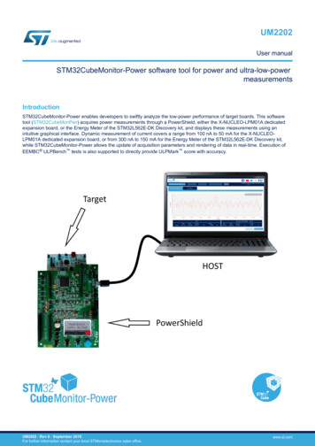
AN4758Memory protection descriptionThe gray areas in Figure 1 are an example of a dual bank organization with two writeprotected (WRP) regions with 2-Kbyte granularity.Figure 1. Two write protected regions per Flash bank0x080000000x08080000WPR1 0WPR0 0WPR1 1WPR0 10x0807FFFF0x080FFFFFBank 2Bank 1MS39956V1The protected area cannot be neither erased nor programmed, any write request generatesa Write protection error. The WRPERR flag is set by hardware when an address to beerased/programmed belongs to a write-protected part of the Flash memory. As an example,the mass erase of a Flash memory where at least one page is write protected is not possibleand the WRPERR flag is set.Enabling or disabling write protection can be managed either by embedded user code or byusing STM32CubeProgrammer software and debug interfaces.1.2.2SRAM2 CCM-SRAM write protectionThe 32 Kbytes of SRAM2 in STM32L4/L4 can be write-protected independently by 1-Kbytepages. The setting of this protection is controlled by a 32-bit system configuration registerand, once enabled, only a system reset can disable it.In STM32G4 the CCM-SRAM can be write-protected by 1-Kbyte segments (32 Kbytes forCat3 device, 10 Kbytes for Cat2 device).For STM32WB the 32 Kbytes of SRAM2a and 32 Kbytes of SRAM2b can be independentlywrite-protected by 1-Kbyte pages, controlled by two 32-bit system configuration registers.AN4758 Rev 69/4342
Memory protection descriptionAN47581.3Proprietary code readout protection (PCROP)1.3.1PCROP protection overviewThe PCROP is a read and write protection of an IP code in Flash memory. It preventsproprietary code from possible modification or readout by the end-user code, debugger toolsor RAM trojan code.Any read or write request generates a Read or Write protection error: The WRPERR flag is set by hardware when an address to be erased/programmedbelongs the PCROP-ed part of the Flash memory. The RDERR flag is set when a read access through the D-bus is performed to aPCROP-ed area. Along with these flags, an interrupt can be raised if enabled by ERRIE bit in theFLASH CR register.The protected IP code can be easily called by the end-user application and still be protectedagainst direct access to the IP code itself. Then PCROP does not prevent protected codesfrom being executed.The PCROP area is set with a fine granularity of 8 bytes, so that no Flash memory iswasted.Figure 2. Flash memory map with PCROP-ed areaUser-code start@User codeUser-code end@PCROP start@PCROP-edIP-Code areaCan be one ormore sectorsPCROP end@MS38228V11.3.2How to enable PCROP protection?On STM32L4/L4 Series, one area per bank can be selected with 64-bit granularity.In STM32G4 Series, depending of the DBANK mode, one PCROP zone per bank (in dualbank mode) or two PCROP zones (for all memory) can be defined.10/43AN4758 Rev 6
AN4758Memory protection descriptionIn STM32WB Series, up to two PCROP areas can be selected with a 2-Kbyte granularity.Each PCROP area is defined by a start page offset and an end page offset related to thephysical Flash memory bank base address.To activate the PCROP, start and end address of the protected area shall be programmed inthe Flash memory option bytes registers: PCROP1SR: PCROP area start address bank 1 PCROP1ER: PCROP area end address bank 1 PCROP2SR: PCROP area start address bank 2 PCROP2ER: PCROP area end address bank 2Table 2 specifies how registers values determine the read-out protection area:Table 2. Protection area vs. register valuesPCROP register valuesPCROP protection areaPCROPxSR PCROPxERMemory bank fully protectedPCROPxSR PCROPxERNo PCROP area (no protection)PCROPxSR PCROPxERArea between PCROPxSR and PCROPxER is protectedAn additional option bit (PCROP RDP PCROP1ER [31]) allows to select if the PCROParea is erased or not when the RDP protection is changed from Level 1 to Level 0. Thisoption is set for both memory banks.For more details on PCROP enabling refer to the example PCROP ENABLE() functiondescribed in the provided FW package (Step1-ST Customer level n project main.c file).1.3.3How to disable PCROP protection?PCROP can only be disabled if RDP level is 1 or 0. If RDP is set to Level 2, PCROP can nomore be disabled; all the option bytes are frozen and can no longer be modified. As a result,PCROPed regions can never be erased or modified, so the protection becomes permanent.The only way to disable PCROP on a protected region, is by decreasing RDP from Level 1to Level 0 and deactivate the programmed area at the same time (in embedded SW, setPCROPxSR PCROPxER).If PCROP RDP is set, a mass erase of the Flash main memory is performed. The backupregisters in the RTC and the SRAM2 / CCM-SRAM are also erased.If the bit PCROP RDP is cleared, the full mass erase is replaced by a partial mass erasethat does successive page erases in the bank where PCROP is active, except for the pagesprotected by PCROP. This is done in order to keep the PCROP code.Use STM32CubeProgrammerDuring application development user may need to disable PCROP or global RDP protectionusing alternatives to embedded Flash memory code. STM32CubeProgrammer tool is asimple method for disabling or enabling protection using debug interfaces as JTAG or SWDwithout the need for developing dedicated functions. Figures 3 to 5 show how to modifyoption bytes.AN4758 Rev 611/4342
Memory protection descriptionAN4758Figure 3. User interface to modify the RDP levelFigure 4. User interface to activate PCROP RDP and activate a PCROP areaFigure 5. User interface to program a Write protection areaFor more details on how to use STM32CubeProgrammer software refer to user manualUM2237 available on the Help section of the tool or at www.st.com.1.3.4PCROP-ed IP code compilationPCROP-ed regions are protected against data bus (D-Code) read accesses, so only codeexecution is allowed (instruction fetch through I-Code bus) while data reading is notpossible. The protected IP code is then unable to access the associated data values storedin the same area such as literal pools or constants fetched from Flash memory through theD-Code bus during the execution.12/43AN4758 Rev 6
AN4758Memory protection descriptionLiteral poolsCompilation option must be used to avoid the use of literal pools that would be placed in thecode section otherwise. Compilation option is further detailed in Section 2.Constant dataNon-volatile data used by the IP code, must be placed in a specific memory region outsidethe PCROP-ed area. The IP code developer must provide the memory map with theseconstant data regions. It is advised to write-protect these sections.1.3.5PCROP-ed IP code dependencyProtected IP code can call functions from libraries located in user code region and outside ofPCROP-ed area. In this case the IP code contains the related functions addresses allowingPC (program counter) to jump to these functions when executing IP code. These addressesare unchangeable once the IP code is PCROP-ed. Consequently, each called function mustbe located (outside of PCROP-ed region) at its corresponding fix address written in thePCROP-ed IP code else, PC jumps to an invalid address and IP code will not work correctly.To be fully independent, protected IP code has to be placed together with all its relatedfunctions.Figure 6 shows an example where PCROP-ed Function A() is calling a Function B() (lightblue) located at a fixed address (in green) outside the PCROP-ed region.Figure 6. PCROP-ed code calling a function located outside the PCROP-ed regionUser-code start@Function B fixed@Function B(){ ; ; ;}User code regionFunction A(){Function B();}PCROP regionUser-code end@PCROP start@PCROP end@MS38280V1AN4758 Rev 613/4342
Memory protection description1.4Other protections1.4.1FirewallAN4758The Firewall is a protection feature available on the STM32L4/L4 Series. Associated to theother Flash memory protections, it provides an increased level of protection for part of codeand data coming from a third party.The user may want to protect some sensitive algorithms using confidential associated data(e.g. cryptographic keys, secured algorithms and associated variables) somewhere in thememory mapping, and/or to manage exactly when the user code is going to access thistrusted area and when this secure area is going to jump back to the non-protected user-code execution. The firewall fills up exactly this role of accesses monitoring (instructionfetches, read, write operations) and generates reset if some non-expected accesses aredetected during the code execution to kill immediately any intrusive action inside theprotected areas.Refer to AN4729 for mode detailed description of the feature.1.4.2Securable memory area for the STM32G4 SeriesThe securable memory area defines an area of code that can be executed only once atboot, and never again unless a new reset occurs.The main purpose of this memory area is to protect a specific part of Flash memory againstundesired access. It is dedicated to executing trusted code such as secure key storage orsafe boot.14/43AN4758 Rev 6
AN47582PCROP examplePCROP exampleThe firmware example provided with this application note illustrates a use case of PCROPprotection feature. All required steps for developing this firmware are detailed in this section.This example has been developed for the STM32L4 Series but it is easily portable to theSTM32L4 , STM32G4 and STM32WB Series.2.1Requirements2.1.1Hardware requirementsThe hardware required to run this example is the following:2.1.2 an STM32L4-discovery board (RevB or RevC) with embedded STM32L476VG MCU a mini-USB cable to power the board and to connect the discovery embedded STLINKfor debugging and programming.Software requirementsThe following software tools are required: IAR Embedded Workbench (v7.40.3) or Keil µvision IDE(v5.14.0) STM32CubeProgrammer (v2.5.0), to enable or disable PCROP protection.2.2Description2.2.1Scenario overviewThis example describes a use case where an ST customer - Level n providespreprogrammed STM32L476VG MCUs with a critical IP code to an ST customer - Leveln 1. The IP code has to be protected by activating PCROP, allowing ST customer - Leveln 1 to use its functions (without the ability to read or modify it) to program the end userapplication.ST customer - Level n must provide with preloaded STM32 MCUs the following inputs: Flash memory map defining the exact protected IP code location, as well as constantdata location. Header file that has to be included in ST customer - Level n 1 project containing IPcode functions definition to be called in End User code. Symbol definition file containing IP code function symbols.AN4758 Rev 615/4342
PCROP exampleAN4758The described use case is schematized in Figure 7.Figure 7. STM32L4 PCROP flow exampleST Customer – Level nPrograms protected IP-CodeCustomer – Level n 1Programs End user Codeusing IP-Code functionsEnd user applicationMS38231V1An OEM (original equipment manufacturer) can be the ST customer - Level n usingSTM32L4 microcontrollers. The OEM provides preprogrammed MCUs to the ST customer - Level n 1, which can be the one making the end user product, as in Figure 8.Figure 8. Example of an ST customer - Level n and level n 1OEMST Customer level nProvidespreprogrammedSTM32L4 MCUsProvidesSTM32L4MCUsEND CUSTOMERST Customer level n 1MS39958V116/43AN4758 Rev 6
AN47582.2.2PCROP examplePCROP-ed IP code: FIR low-pass filterAs an example FIR let us consider a low-pass filter algorithm from CMSIS-DSP library asthe IP code to be protected, focusing on detailing how to protect and call this IP codeexample, without providing any details on the functions.The FIR low-pass filter removes high frequency signal components from the input.The input signal is a sum of two sine waves: 1 kHz and 15 kHz. The low-pass filter (with apreconfigured cutoff frequency of 6 kHz) eliminates the 15 kHz signal leaving the 1 kHz sinewave at the output.Figure 9 shows the FIR low-pass filter block diagram.Figure 9. FIR low-pass filter function block diagramtestOutputtestInput f32 1kHz 15kHzFIR lowpass filter ()MS38230V1Used CMSIS DSP software library functions: arm fir init f32(): initialization function to configure the filter, described inarm fir init f32.c file; arm fir f32(): the elementary function representing the FIR filter, described inarm fir f32.c file.The following function has been created using the CMSIS DSP functions described above: FIR lowpass filter(): the global function representing the FIR filter, described infir filter.c file.The FPU and DSP embedded in STM32L4 microcontrollers are used for signal processingand floating point calculation to output the correct signal.For more details on FIR functions refer to CMSIS documentation in“Drivers/CMSIS/Documentation/DSP” directory included in the associated softwarepackage.AN4758 Rev 617/4342
PCROP example2.2.3AN4758Software settingsThis application note describes two projects (Figure 10).Figure 10. PCROP example software settingsProjectST Customer level nProjectST Customer level n 1Conf 1Conf 2Conf 959V1Project 1: STEP1-ST Customer level nThis project shows an example of how an ST customer - Level n can place, protect andexecute its IP code and how to generate IP code related files as header and symboldefinition files to be provided to ST customer - Level n 1.This project includes two different project configurations: PCROP-IP-Code-XO: in this configuration the compiler is configured to generate anexecute-only IP code avoiding any data read from it. PCROP-IP-Code: in this configuration the IP code is compiled without avoiding data(literal pools) generation. This configuration is dedicated to testing purposes in order toshow that PCROP-ed IP code must be an execute-only code.Project 2: STEP2-ST Customer level n 1This project shows an example of how an ST customer - Level n 1 with a preprogrammedSTM32L476VG with a PCROP-ed IP code can create its own end user application using theprotected IP code functions.2.3Development step 1: ST customer - Level nAt this stage the ST customer - Level n:18/43 generates an ex
Firewall: access protection to sensitive code and data against external processes. This application note provides a description of the Flash memory protection features, focusing on the PCROP technique, and providing a basic example of it. Firewall protection (available on STM32L4 and STM32L4 Series) is described in AN4729 " STM32L0/L4