Transcription
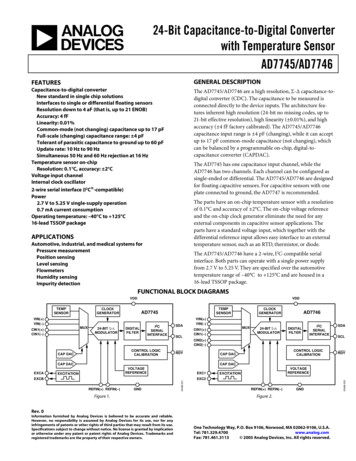
24-Bit Capacitance-to-Digital Converterwith Temperature SensorAD7745/AD7746FEATURESGENERAL DESCRIPTIONCapacitance-to-digital converterNew standard in single chip solutionsInterfaces to single or differential floating sensorsResolution down to 4 aF (that is, up to 21 ENOB)Accuracy: 4 fFLinearity: 0.01%Common-mode (not changing) capacitance up to 17 pFFull-scale (changing) capacitance range: 4 pFTolerant of parasitic capacitance to ground up to 60 pFUpdate rate: 10 Hz to 90 HzSimultaneous 50 Hz and 60 Hz rejection at 16 HzTemperature sensor on-chipResolution: 0.1 C, accuracy: 2 CVoltage input channelInternal clock oscillator2-wire serial interface (I2C -compatible)Power2.7 V to 5.25 V single-supply operation0.7 mA current consumptionOperating temperature: –40 C to 125 C16-lead TSSOP packageThe AD7745/AD7746 are a high resolution, Σ-Δ capacitance-todigital converter (CDC). The capacitance to be measured isconnected directly to the device inputs. The architecture features inherent high resolution (24-bit no missing codes, up to21-bit effective resolution), high linearity ( 0.01%), and highaccuracy ( 4 fF factory calibrated). The AD7745/AD7746capacitance input range is 4 pF (changing), while it can acceptup to 17 pF common-mode capacitance (not changing), whichcan be balanced by a programmable on-chip, digital-tocapacitance converter (CAPDAC).The AD7745 has one capacitance input channel, while theAD7746 has two channels. Each channel can be configured assingle-ended or differential. The AD7745/AD7746 are designedfor floating capacitive sensors. For capacitive sensors with oneplate connected to ground, the AD7747 is recommended.The parts have an on-chip temperature sensor with a resolutionof 0.1 C and accuracy of 2 C. The on-chip voltage referenceand the on-chip clock generator eliminate the need for anyexternal components in capacitive sensor applications. Theparts have a standard voltage input, which together with thedifferential reference input allows easy interface to an externaltemperature sensor, such as an RTD, thermistor, or diode.APPLICATIONSAutomotive, industrial, and medical systems forPressure measurementPosition sensingLevel sensingFlowmetersHumidity sensingImpurity detectionThe AD7745/AD7746 have a 2-wire, I2C-compatible serialinterface. Both parts can operate with a single power supplyfrom 2.7 V to 5.25 V. They are specified over the automotivetemperature range of –40 C to 125 C and are housed in a16-lead TSSOP package.FUNCTIONAL BLOCK DIAGRAMSVDDTEMPSENSORCLOCKGENERATORVDDVIN( )VIN(–)MUXCIN1( )CIN1(–)24-BIT Σ- ERFACESDASCLCLOCKGENERATORAD7746VIN( )VIN(–)MUXCIN1( )CIN1(–)24-BIT Σ- ( )CIN2(–)CONTROL LOGICCALIBRATIONCAP DACRDYRDYCAP DACVOLTAGEREFERENCEEXCBREFIN( ) REFIN(–)GNDFigure NEXC2REFIN( ) REFIN(–)GNDFigure 2.Rev. 0Information furnished by Analog Devices is believed to be accurate and reliable.However, no responsibility is assumed by Analog Devices for its use, nor for anyinfringements of patents or other rights of third parties that may result from its use.Specifications subject to change without notice. No license is granted by implicationor otherwise under any patent or patent rights of Analog Devices. Trademarks andregistered trademarks are the property of their respective owners.One Technology Way, P.O. Box 9106, Norwood, MA 02062-9106, U.S.A.Tel: 781.329.4700www.analog.comFax: 781.461.3113 2005 Analog Devices, Inc. All rights reserved.05468-002CAP DACEXCACONTROL LOGICCALIBRATIONCAP DAC
AD7745/AD7746TABLE OF CONTENTSSpecifications. 3Cap Gain Calibration Register. 19Timing Specifications. 5Volt Gain Calibration Register . 19Absolute Maximum Ratings. 6Circuit Description. 20Pin Configurations and Function Descriptions . 7Overview . 20Typical Performance Characteristics . 8Capacitance-to-Digital Converter . 20Output Noise and Resolution Specifications . 11Excitation Source. 20Serial Interface . 12CAPDAC . 21Read Operation. 12Single-Ended Capacitive Input. 21Write Operation. 12Differential Capacitive Input . 21AD7745/AD7746 Reset . 13Parasitic Capacitance to Ground. 22General Call. 13Parasitic Resistance to Ground. 22Register Descriptions . 14Parasitic Parallel Resistance . 22Status Register . 15Parasitic Serial Resistance . 23Cap Data Register. 15Capacitive Gain Calibration . 23VT Data Register . 15Capacitive System Offset Calibration . 23Cap Set-Up Register . 16Internal Temperature Sensor . 23VT Set-Up Register . 16External Temperature Sensor . 24EXC Set-Up Register . 17Voltage Input. 24Configuration Register . 18VDD Monitor . 24Cap DAC A Register. 19Typical Application Diagram. 24Cap DAC B Register. 19Outline Dimensions . 25Cap Offset Calibration Register. 19Ordering Guide . 25REVISION HISTORY4/05—Revision 0: Initial VersionRev. 0 Page 2 of 28
AD7745/AD7746SPECIFICATIONSVDD 2.7 V to 3.6 V or 4.75 V to 5.25 V; GND 0 V; EXC 32 kHz; EXC VDD/2; –40 C to 125 C, unless otherwise noted.Table 1.ParameterCAPACITIVE INPUTConversion Input RangeIntegral Nonlinearity (INL)2No Missing Codes2Resolution, p-pResolution EffectiveOutput Noise, rmsAbsolute Error3Offset Error2, 4System Offset Calibration Range2Offset Drift vs. TemperatureGain Error5Gain Drift vs. Temperature2Allowed Capacitance to GND2Power Supply RejectionNormal Mode RejectionChannel-to-Channel IsolationCAPDACFull RangeResolution6Drift vs. Temperature2EXCITATIONFrequencyVoltage Across CapacitanceMinMax 4.096 0.012416.5192 432 60.1 0.5 2UnitTest Conditions/CommentspF1% of FSRBitBitBitaF/ HzfF1aF1Factory calibratedpFaF/ C% of FSppm of FS/ CpFfF/VdBdBdB28pFfFppm of FS/ C 40kHzVVVVmV100pF 2 C C C32 VDD/8 VDD/4 VDD 3/8 VDD/2Average DC Voltage AcrossCapacitanceAllowed Capacitance to GND2TEMPERATURE SENSOR7ResolutionError2VOLTAGE INPUT7Differential VIN Voltage RangeAbsolute VIN Voltage2Integral Nonlinearity (INL)No Missing Codes2Resolution, p-pTyp VREF16VVppm of FSBitBitsOutput Noise3µV rmsOffset ErrorOffset Drift vs. TemperatureFull-Scale Error2, 9 3150.025µVnV/ C% of FSGND 0.03VDD 0.03 15 3240.1Rev. 0 Page 3 of 28Conversion time 62 msConversion time 62 ms, see Table 5Conversion time 62 ms, see Table 5See Table 525 C, VDD 5 V, after offset calibrationAfter system offset calibration,Excluding effect of noise425 C, VDD 5 VSee Figure 9 and Figure 1050 Hz 1%, conversion time 62 ms60 Hz 1%, conversion time 62 msAD7746 only7-bit CAPDACConfigurable via digital interfaceSee Figure 11VREF internalInternal temperature sensorExternal sensing diode8VREF internal or VREF 2.5 VConversion time 122.1 msConversion time 62 msSee Table 6 and Table 7Conversion time 62 msSee Table 6 and Table 7
AD7745/AD7746ParameterFull-Scale Drift vs. TemperatureMinTyp50.5300 508090755095Max1.1691.1750.1GND 0.032.5Average VIN Input CurrentAnalog VIN Input Current DriftPower Supply RejectionPower Supply RejectionNormal Mode RejectionCommon-Mode RejectionINTERNAL VOLTAGE REFERENCEVoltageDrift vs. TemperatureEXTERNAL VOLTAGE REFERENCE INPUTDifferential REFIN Voltage2Absolute REFIN Voltage2Average REFIN Input CurrentAverage REFIN Input Current DriftCommon-Mode RejectionSERIAL INTERFACE LOGIC INPUTS(SCL, SDA)VIH Input High VoltageVIL Input Low VoltageHysteresisInput Leakage Current (SCL)OPEN-DRAIN OUTPUT (SDA)VOL Output Low VoltageIOH Output High Leakage CurrentLOGIC OUTPUT (RDY)VOL Output Low VoltageVOH Output High VoltageVOL Output Low VoltageVOH Output High VoltagePOWER REQUIREMENTSVDD-to-GND VoltageTest Conditions/CommentsInternal referenceExternal reference1.171Vppm/ CTA 25 CVDDVDD 0.03VVnA/VpA/V/ CdB400 50802.10.8Internal reference, VIN VREF/2External reference, VIN VREF/250 Hz 1%, conversion time 122.1 ms60 Hz 1%, conversion time 122.1 msVIN 1 VVVmVµA150 0.1 10.4V0.11µAISINK 6.0 mAVOUT VDD0.4VVVVISINK 1.6 mA, VDD 5 VISOURCE 200 µA, VDD 5 VISINK 100 µA, VDD 3 VISOURCE 100 µA, VDD 3 VVVµAµAµAµAVDD 5 V, nominalVDD 3.3 V, nominalDigital inputs equal to VDD or GNDVDD 5 VVDD 3.3 VDigital inputs equal to VDD or GND4.00.4VDD – 0.64.752.75.253.6850IDD CurrentIDD Current Power-Down ModeUnitppm of FS/ Cppm of FS/ CnA/VpA/V/ CdBdBdBdBdB7507000.521Capacitance units: 1 pF 10-12 F; 1 fF 10-15 F; 1 aF 10-18 F.Specification is not production tested, but is supported by characterization data at initial product release.3Factory calibrated. The absolute error includes factory gain calibration error, integral nonlinearity error, and offset error after system offset calibration, all at 25 C. Atdifferent temperatures, compensation for gain drift over temperature is required.4The capacitive input offset can be eliminated using a system offset calibration. The accuracy of the system offset calibration is limited by the offset calibration registerLSB size (32 aF) or by converter system p-p noise during the system capacitive offset calibration, whichever is greater. To minimize the effect of the converter system noise, longer conversion times should be used for system capacitive offset calibration. The system capacitance offset calibration range is 1 pF, the largeroffset can be removed using CAPDACs.5The gain error is factory calibrated at 25 C. At different temperatures, compensation for gain drift over temperature is required.6The CAPDAC resolution is seven bits in the actual CAPDAC full range. Using the on-chip offset calibration or adjusting the capacitive offset calibration register canfurther reduce the CIN offset or the unchanging CIN component.7The VTCHOP bit in the VT SETUP register must be set to 1 for the specified temperature sensor and voltage input performance.8Using an external temperature sensing diode 2N3906, with nonideality factor nf 1.008, connected as in Figure 41, with total serial resistance 100 Ω.9Full-scale error applies to both positive and negative full scale.2Rev. 0 Page 4 of 28
AD7745/AD7746TIMING SPECIFICATIONSVDD 2.7 V to 3.6 V, or 4.75 V to 5.25 V; GND 0 V; Input Logic 0 0 V; Input Logic 1 VDD; –40 C to 125 C, unless otherwise noted.Table 2.ParameterSERIAL INTERFACE1, 2SCL FrequencySCL High Pulse Width, tHIGHSCL Low Pulse Width, tLOWSCL, SDA Rise Time, tRSCL, SDA Fall Time, tFHold Time (Start Condition), tHD;STASet-Up Time (Start Condition), tSU;STAData Set-Up Time, tSU;DATData Set-Up Time, tSU;DATSet-Up Time (Stop Condition), tSU;STOData Hold Time, tHD;DAT (Master)Bus-Free Time (Between Stop and Start Condition, µsµsµsµs0.30.30.60.60.250.350.601.3Test Conditions/CommentsSee Figure 3After this period, the first clock is generatedRelevant for repeated start conditionVDD 3.0 VVDD 3.0 VSample tested during initial release to ensure compliance.All input signals are specified with input rise/fall times 3 ns, measured between the 10% and 90% points. Timing reference points at 50% for inputs and outputs.Output load 10 :DATtSU:STOSDAtBUFPSSFigure 3. Serial Interface Timing DiagramRev. 0 Page 5 of 28P05468-0031Min
AD7745/AD7746ABSOLUTE MAXIMUM RATINGSTA 25 C, unless otherwise noted.Table 3.ParameterPositive Supply Voltage VDD to GNDVoltage on any Input or Output Pin toGNDESD Rating (ESD Association Human BodyModel, S5.1)Operating Temperature RangeStorage Temperature RangeJunction TemperatureTSSOP Package θJA,(Thermal Impedance-to-Air)TSSOP Package θJC,(Thermal Impedance-to-Case)Lead Temperature, SolderingVapor Phase (60 sec)Infrared (15 sec)Rating 0.3 V to 6.5 V–0.3 V to VDD 0.3 V2000 V–40 C to 125 C–65 C to 150 C150 C128 C/WStresses above those listed under Absolute Maximum Ratingsmay cause permanent damage to the device. This is a stressrating only and functional operation of the device at these orany other conditions above those indicated in the operationalsection of this specification is not implied. Exposure to absolutemaximum rating conditions for extended periods may affectdevice reliability.14 C/W215 C220 CESD CAUTIONESD (electrostatic discharge) sensitive device. Electrostatic charges as high as 4000 V readily accumulate on thehuman body and test equipment and can discharge without detection. Although this product featuresproprietary ESD protection circuitry, permanent damage may occur on devices subjected to high energyelectrostatic discharges. Therefore, proper ESD precautions are recommended to avoid performancedegradation or loss of functionality.Rev. 0 Page 6 of 28
AD7745/AD7746PIN CONFIGURATIONS AND FUNCTION DESCRIPTIONSRDYSCL 116 SDA215 NCRDY16 SDA215 NC14 VDDEXCA 313 GNDTOP VIEWREFIN( ) 5 (Not to Scale) 12 VIN(–)EXCB 413 GNDTOP VIEWREFIN( ) 5 (Not to Scale) 12 VIN(–)REFIN(–) 611 VIN( )REFIN(–) 6EXCA 3EXCB 4AD774514 VDDAD774611 VIN( )10 NCCIN1(–) 710 CIN2(–)CIN1( ) 89NCCIN1( ) 89NC NO CONNECT05468-004CIN1(–) 7NC NO CONNECTFigure 4. AD7745 Pin Configuration (16-Lead TSSOP)CIN2( )05468-005SCL 1Figure 5. AD7746 Pin Configuration (16-Lead TSSOP)Table 4. Pin Function DescriptionsPin No.1MnemonicSCL2RDY3, 4EXCA, EXCB5, 6REFIN( ),REFIN(–)7CIN1(–)8CIN1( )9, 10(AD7745)9(AD7746)10(AD7746)11, 12NC1314GNDVDD1516NCSDACIN2( )CIN2(–)VIN( ), VIN(–)DescriptionSerial Interface Clock Input. Connects to the master clock line. Requires pull-up resistor if not alreadyprovided in the system.Logic Output. A falling edge on this output indicates that a conversion on enabled channel(s) has beenfinished and the new data is available. Alternatively, the status register can be read via the 2-wire serialinterface and the relevant bit(s) decoded to query the finished conversion. If not used, this pin should be leftas an open circuit.CDC Excitation Outputs. The measured capacitance is connected between one of the EXC pins and one of theCIN pins. If not used, these pins should be left as an open circuit.Differential Voltage Reference Input for the Voltage Channel (ADC). Alternatively, the on-chip internalreference can be used for the voltage channel. These reference input pins are not used for conversion oncapacitive channel(s) (CDC). If not used, these pins can be left as an open circuit or connected to GND.CDC Negative Capacitive Input in Differential Mode. This pin is internally disconnected in single-ended CDCconfiguration. If not used, this pin can be left as an open circuit or connected to GND.CDC Capacitive Input (in Single-Ended Mode) or Positive Capacitive Input (in Differential Mode). Themeasured capacitance is connected between one of the EXC pins and one of the CIN pins. If not used, this pincan be left as an open circuit or connected to GND.Not Connected. This pin should be left as an open circuit.CDC Second Capacitive Input (in Single-Ended Mode) or Positive Capacitive Input (in Differential Mode). If notused, this pin can be left open circuit or connected to GND.CDC Negative Capacitive Input in Differential Mode. This pin is internally disconnected in a single-ended CDCconfiguration. If not used, this pin can be left as an open circuit or connected to GND.Differential Voltage Input for the Voltage Channel (ADC). These pins are also used to connect an externaltemperature sensing diode. If not used, these pins can be left as an open circuit or connected to GND.Ground Pin.Power Supply Voltage. This pin should be decoupled to GND, using a low impedance capacitor, for examplein combination with a 10 µF tantalum and a 0.1 µF multilayer ceramic.Not Connected. This pin should be left as an open circuit.Serial Interface Bidirectional Data. Connects to the master data line. Requires a pull-up resistor if not providedelsewhere in the system.Rev. 0 Page 7 of 28
AD7745/AD7746TYPICAL PERFORMANCE CHARACTERISTICS181002.7V3V3.3V5V1614CAPACITANCE ERROR 23405468-017INL ANCE CIN PIN TO GND (pF)INPUT CAPACITANCE (pF)Figure 6. Capacitance Input Integral Nonlinearity,VDD 5 V, the Same Configuration as in Figure 31Figure 9. Capacitance Input Error vs. Capacitance between CIN and GND.CIN( ) to EXC 4 pF, CIN( ) to EXC 0 pF, VDD 2.7 V, 3 V, 3.3 V, and 5 V,the Same Configuration as in Figure 33200018GAIN TC –26ppm/ C161000CAPACITANCE ERROR 205468-015–3000–502.7V1205468-018GAIN ERROR (ppm)140150–20TEMPERATURE ( C)50100150200250300350400500450CAPACITANCE CIN PIN TO GND (pF)Figure 7. Capacitance Input Offset Drift vs. Temperature,VDD 5 V, CIN and EXC Pins Open CircuitFigure 10. Capacitance Input Error vs. Capacitance between CIN and GND,CIN( ) to EXC 21 pF, CIN( ) to EXC 23 pF, VDD 2.7 V, 3 V, 3.3 V, and 5 V,the Same Configuration as in Figure 341005752.7V4CAPACITANCE ERROR .3V21005468-016–753V05468-019OFFSET ERROR (aF)50–11500TEMPERATURE ( C)50100150200250300350400450500CAPACITANCE EXC PIN TO GND (pF)Figure 8. Capacitance Input Gain Drift vs. Temperature,VDD 5 V, CIN( ) to EXC 4 pF, the Same Configuration as in Figure 30Figure 11. Capacitance Input Error vs. Capacitance between EXC and GND,CIN( ) to EXC 21 pF, CIN( ) to EXC 23 pF, VDD 2.7 V, 3 V, 3.3 V, and 5 V,the Same Configuration as in Figure 34Rev. 0 Page 8 of 28
AD7745/AD7746086–2CAPACITANCE ERROR ��10–12–250 –200 –150 –100–5005010015020005468-031CAPACITANCE ERROR (fF)4–10250102CIN LEAKAGE TO GND (nA)34567SERIAL RESISTANCE (kΩ)Figure 12. Capacitance Input Error vs. Leakage Current to GND,CIN( ) to EXC 4 pF, CIN( ) to EXC 0 pF,VDD 2.7 V and 3 VFigure 15. Capacitance Input Error vs. Serial Resistance,CIN( ) to EXC 21 pF, CIN( ) to EXC 23 pF, VDD 5 V,the Same Configuration as in Figure 34.0.2860CAPACITANCE ERROR 468-0303.3V–10–12–250 –200 –150 TANCE ERROR (fF)43.03.54.04.55.05.5VDD (V)CIN LEAKAGE TO GND (nA)Figure 16. Capacitance Input Power Supply Rejection (PSR),CIN( ) to EXC 4 pF, the Same Configuration as in Figure 30Figure 13. Capacitance Input Error vs. Leakage Current to GND,CIN( ) to EXC 4 pF, CIN( ) to EXC 0 pF,VDD 3.3 V and 5 V100.20CAPDAC CODE DNL 0.050–0.05–0.10–0.1505468-033CAPACITANCE ERROR (pF)0.151–0.201000000PARALLEL RESISTANCE (MΩ)163248648096112CAPDAC CODEFigure 14. Capacitance Input Error vs. Resistance in Parallelwith Measured CapacitanceFigure 17. CAPDAC Differential Nonlinearity (DNL)Rev. 0 Page 9 of 28128
AD7745/AD77462.001.5–201.0GAIN (dB)ERROR ( 0050TEMPERATURE ( C)100150200250300350400INPUT SIGNAL FREQUENCY (Hz)Figure 21. Capacitance Channel Frequency Response,Conversion Time 62 msFigure 18. Internal Temperature Sensor Error vs. Temperature1.000.5–200GAIN (dB)ERROR ( –120150050TEMPERATURE ( N (dB)–2005468-036GAIN (dB)0200200Figure 22. Capacitance Channel Frequency Response,Conversion Time 109.6 ms0100150INPUT SIGNAL FREQUENCY (Hz)Figure 19. External Temperature Sensor Error vs. T SIGNAL FREQUENCY (Hz)INPUT SIGNAL FREQUENCY (Hz)Figure 20. Capacitance Channel Frequency Response,Conversion Time 11 msFigure 23. Voltage Channel Frequency Response,Conversion Time 122.1 msRev. 0 Page 10 of 28400
AD7745/AD7746OUTPUT NOISE AND RESOLUTION SPECIFICATIONSThe AD7745/AD7746 resolution is limited by noise. The noiseperformance varies with the selected conversion time.Table 5 shows typical noise performance and resolution for thecapacitive channel. These numbers were generated from 1000data samples acquired in continuous conversion mode, at anexcitation of 32 kHz, VDD/2, and with all CIN and EXC pinsconnected only to the evaluation board (no external capacitors.)Table 6 and Table 7 show typical noise performance andresolution for the voltage channel. These numbers weregenerated from 1000 data samples acquired in continuousconversion mode with VIN pins shorted to ground.RMS noise represents the standard deviation and p-p noiserepresents the difference between minimum and maximumresults in the data. Effective resolution is calculated from rmsnoise, and p-p resolution is calculated from p-p noise.Table 5. Typical Capacitive Input Noise and Resolution vs. Conversion TimeConversionTime (ms)11.011.920.038.062.077.092.0109.6Output DataRate (Hz)90.983.850.026.316.113.010.99.1–3dB Frequency(Hz)87.279.043.621.813.810.58.98.0RMS Noise(aF/ Hz)4.33.11.81.61.51.51.51.5RMSNoise (aF)40.027.312.27.35.44.94.44.2P-PNoise (aF)212.4137.782.550.333.728.327.827.3Effective P ble 6. Typical Voltage Input Noise and Resolution vs. Conversion Time, Internal Voltage ReferenceConversionTime (ms)20.132.162.1122.1Output DataRate (Hz)49.831.216.18.2–3dB Frequency(Hz)26.415.98.04.0RMS Noise(µV)11.47.14.03.0P-P Noise(µV)62422820Effective Resolution(Bits)17.618.319.119.5P-P Resolution(Bits)15.215.716.316.8Table 7. Typical Voltage Input Noise and Resolution vs. Conversion Time, External 2.5 V Voltage ReferenceConversionTime (ms)20.132.162.1122.1Output DataRate (Hz)49.831.216.18.2–3dB Frequency(Hz)26.415.98.04.0RMS Noise(µV)14.96.33.32.1P-P Noise(µV)95422215Rev. 0 Page 11 of 28Effective Resolution(Bits)18.319.620.521.1P-P Resolution(Bits)15.616.817.718.3
AD7745/AD7746SERIAL INTERFACEThe AD7745/AD7746 supports an I2C-compatible 2-wire serialinterface. The two wires on the I2C bus are called SCL (clock)and SDA (data). These two wires carry all addressing, control,and data information one bit at a time over the bus to allconnected peripheral devices. The SDA wire carries the data,while the SCL wire synchronizes the sender and receiver duringthe data transfer. I2C devices are classified as either master orslave devices. A device that initiates a data transfer message iscalled a master, while a device that responds to this message iscalled a slave.To control the AD7745/AD7746 device on the bus, thefollowing protocol must be followed. First, the master initiates adata transfer by establishing a start condition, defined by ahigh-to-low transition on SDA while SCL remains high. Thisindicates that the start byte follows. This 8-bit start byte is madeup of a 7-bit address plus an R/W bit indicator.All peripherals connected to the bus respond to the startcondition and shift in the next 8 bits (7-bit address R/W bit).The bits arrive MSB first. The peripheral that recognizes thetransmitted address responds by pulling the data line lowduring the ninth clock pulse. This is known as the acknowledgebit. All other devices withdraw from the bus at this point andmaintain an idle condition. An exception to this is the generalcall address, which is described later in this document. The idlecondition is where the device monitors the SDA and SCL lineswaiting for the start condition and the correct address byte. TheR/W bit determines the direction of the data transfer. A Logic 0LSB in the start byte means that the master writes informationto the addressed peripheral. In this case the AD7745/AD7746becomes a slave receiver. A Logic 1 LSB in the start byte meansthat the master reads information from the addressed peripheral. In this case, the AD7745/AD7746 becomes a slavetransmitter. In all instances, the AD7745/AD7746 acts as astandard slave device on the I2C bus.The start byte address for the AD7745/AD7746 is 0x90 for awrite and 0x91 for a read.READ OPERATIONWhen a read is selected in the start byte, the register that iscurrently addressed by the address pointer is transmitted on tothe SDA line by the AD7745/AD7746. This is then clocked outby the master device and the AD7745/AD7746 awaits anacknowledge from the master.If an acknowledge is received from the master, the address autoincrementer automatically increments the address pointerregister and outputs the next addressed register content on tothe SDA line for transmission to the master. If no acknowledgeis received, the AD7745/AD7746 return to the idle state and theaddress pointer is not incremented.The address pointers’ auto-incrementer allow block data to bewritten or read from the starting address and subsequentincremental addresses.In continuous conversion mode, the address pointers’ autoincrementer should be used for reading a conversion result.That means, the three data bytes should be read using onemultibyte read transaction rather than three separate single bytetransactions. The single byte data read transaction may result inthe data bytes from two different results being mixed. The sameapplies for six data bytes if both the capacitive and thevoltage/temperature channel are enabled.The user can also access any unique register (address) on a oneto-one basis without having to update all the registers. Theaddress pointer register contents cannot be read.If an incorrect address pointer location is accessed or, if the userallows the auto-incrementer to exceed the required registeraddress, the following applies: In read mode, the AD7745/AD7746 continues to outputvarious internal register contents until the master deviceissues a no acknowledge, start, or stop condition. Theaddress pointers’ auto-incrementer’s contents are reset topoint to the status register at Address 0x00 when a stopcondition is received at the end of a read operation. Thisallows the status register to be read (polled) continuallywithout having to constantly write to the address pointer. In write mode, the data for the invalid address is not loadedinto the AD7745/AD7746 registers but an acknowledge isissued by the AD7745/AD7746.WRITE OPERATIONWhen a write is selected, the byte following the start byte isalways the register address pointer (subaddress) byte, whichpoints to one of the internal registers on the AD7745/ AD7746.The address pointer byte is automatically loaded into theaddress pointer register and acknowledged by the AD7745/AD7746. After the address pointer byte acknowledge, a stopcondition, a repeated start condition, or another data byte canfollow from the master.A stop condition is defined by a low-to-high transition on SDAwhile SCL remains high. If a stop condition is ever encounteredby the AD7745/AD7746, it returns to its idle condition and theaddress pointer is reset to Address 0x00.If a data byte is transmitted after the register address pointerbyte, the AD7745/AD7746 load this byte into the register that iscurrently addressed by the address pointer register, send anacknowledge, and the address pointer auto-incrementer automatically increments the address pointer register to the nextinternal register address. Thus, subsequent transmitted databytes are loaded into sequentially incremented addresses.Rev. 0 Page 12 of 28
AD7745/AD7746If a repeated start condition is encountered after the addresspointer byte, all peripherals connected to the bus respondexactly as outlined above for a start condition, that is, a repeatedstart condition is treated the same as a start condition. When amaster device issues
AD7745/AD7746 Rev. 0 Page 3 of 28 SPECIFICATIONS V DD 2.7 V to 3.6 V or 4.75 V to 5.25 V; GND 0 V; EXC 32 kHz; EXC V DD/2; -40 C to 125 C, unless otherwise noted. Table 1. Parameter Min Typ Max Unit Test Conditions/Comments CAPACITIVE INPUT Conversion Input Range 4.096 pF1 Factory calibrated Integral Nonlinearity (INL)2 0.01 % of FSR