Transcription
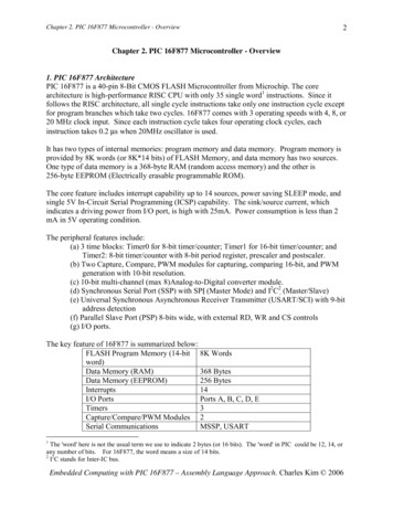
Chapter 2. PIC 16F877 Microcontroller - Overview2Chapter 2. PIC 16F877 Microcontroller - Overview1. PIC 16F877 ArchitecturePIC 16F877 is a 40-pin 8-Bit CMOS FLASH Microcontroller from Microchip. The corearchitecture is high-performance RISC CPU with only 35 single word1 instructions. Since itfollows the RISC architecture, all single cycle instructions take only one instruction cycle exceptfor program branches which take two cycles. 16F877 comes with 3 operating speeds with 4, 8, or20 MHz clock input. Since each instruction cycle takes four operating clock cycles, eachinstruction takes 0.2 µs when 20MHz oscillator is used.It has two types of internal memories: program memory and data memory. Program memory isprovided by 8K words (or 8K*14 bits) of FLASH Memory, and data memory has two sources.One type of data memory is a 368-byte RAM (random access memory) and the other is256-byte EEPROM (Electrically erasable programmable ROM).The core feature includes interrupt capability up to 14 sources, power saving SLEEP mode, andsingle 5V In-Circuit Serial Programming (ICSP) capability. The sink/source current, whichindicates a driving power from I/O port, is high with 25mA. Power consumption is less than 2mA in 5V operating condition.The peripheral features include:(a) 3 time blocks: Timer0 for 8-bit timer/counter; Timer1 for 16-bit timer/counter; andTimer2: 8-bit timer/counter with 8-bit period register, prescaler and postscaler.(b) Two Capture, Compare, PWM modules for capturing, comparing 16-bit, and PWMgeneration with 10-bit resolution.(c) 10-bit multi-channel (max 8)Analog-to-Digital converter module.(d) Synchronous Serial Port (SSP) with SPI (Master Mode) and I2C2 (Master/Slave)(e) Universal Synchronous Asynchronous Receiver Transmitter (USART/SCI) with 9-bitaddress detection(f) Parallel Slave Port (PSP) 8-bits wide, with external RD, WR and CS controls(g) I/O ports.The key feature of 16F877 is summarized below:FLASH Program Memory (14-bit 8K Wordsword)Data Memory (RAM)368 BytesData Memory (EEPROM)256 BytesInterrupts14I/O PortsPorts A, B, C, D, ETimers3Capture/Compare/PWM Modules 2Serial CommunicationsMSSP, USART1The 'word' here is not the usual term we use to indicate 2 bytes (or 16 bits). The 'word' in PIC could be 12, 14, orany number of bits. For 16F877, the word means a size of 14 bits.2 2I C stands for Inter-IC bus.Embedded Computing with PIC 16F877 – Assembly Language Approach. Charles Kim 2006
3Chapter 2. PIC 16F877 Microcontroller - OverviewParallel Communications10-bit Analog-to-Digital ModuleInstruction SetPSP8 channels35 Instructions2. Pin and PackageThere are three package types are available: DIP, PLCC, and QFP. This book assumes that weall use the DIP because of its best fit to breadboard or F PSP1RD2/PSP221Fig 1. PIC 16F877 IC Package: DIPEmbedded Computing with PIC 16F877 – Assembly Language Approach. Charles Kim 2006
4Chapter 2. PIC 16F877 Microcontroller - OverviewTable 1. Pin DescriptionPin#1234567891011121314151617181920Pin NameDescription T1CK1RC1/CCP2RC2/CCP1RC3/SCK/SCLRD0RD1PORTA.0 /Analog Channel 0PORTA.1 /Analog Channel 1PORTA.2 /Analog Channel 2PORTA.3 /Analog Channel 3PORTA.4 / External Clock for Timer 0PORTA.5 /Analog Channel 4PORTE.0 /Analog Channel 5PORTE.1 /Analog Channel 6PORTE.2 /Analog Channel 7 3 5VGNDOscillator Connection /Clock InOscillator Connection / Clock OutPORTC.0 /External Clock for Timer 1PORTC.1 /CCP2PORTC.2 /CCP1PORTC.3 /SCK(for SPI)/SCL(for 353637383940Pin GCRB7/PGDPORTD.2PORTD.3PORTC.4/SDI(for SPI)/SDA(for I2C)PORTC.5 /SDO (for SPI)PORTC.6 /TX (for Serial Com.)PORTC.7 /RX (for Serial Com.)PORTD.4PORTD.5PORTD.6PORTD.7GND 3 V 5 VPORTB.0/External InterruptPORTB.1PORTB.2 /Programming InputPORTB.3PORTB.4PORTB.5PORTB.6 /Debugger/ICSPPORTB.7 /Debugger/ICSP3. Block DiagramThe internal schematic of PIC16F877 is illustrated in the following block diagram. In the blockdiagram, we first see built-in function modules in boxes such as PORTA, PORTB for inputs andoutputs, a 10-bit Analog-to-Digital (AD) module, 3 timer modules (Timer 0, Timer 1, and Timer2), EEPROM, etc. We also see the modules are connected via internal data bus of 8-bit width.This is the reason why 16F877 is called an 8-bit microcontroller. Since the program memory(FLASH) is organized with 14-bit word, it's content is accessed (or fetched) via 14-bit programbus by the instruction register. Instruction registers are not in the file (RAM) area so is notaccessible by program. Another internal register, program counter (PC) accesses the programmemory location ("addressing") via 13 bit information. With 13 bits, the addressing range goesto 213 23*210 8K word.RAM file registers for data are connected via 8-bit data bus. The W register is a user accessibleregister. As you see in the block diagram, W directly accesses the ALU and the 8-bit data bus.As we can see, there should be W involved to move data between modules and inside the fileRAM, except via indirect addressing mode. This means that writing to the output ports is donevia the W register. The details of the indirect addressing are discussed in the PIC instruction.Embedded Computing with PIC 16F877 – Assembly Language Approach. Charles Kim 2006
Chapter 2. PIC 16F877 Microcontroller - Overview5Fig. 2 PIC16F877 Block Diagram4. Program MemoryThe PIC16F877 has a 13-bit program counter (PC) capable of addressing an 8K word ofprogram memory pace, and accessing a location above the physically implemented address willcause a wrap-around.The reset vector is at address 0000 and the interrupt vector is at address 00043. Details of thiswill be discussed through out the book as related subjects pop up.3All addresses are in hexadecimal number unless stated otherwise. Hexadecimal numbers are usually indicated by amultiple-digit number followed by a letter h. In assembly language programming, however, we indicate ahexadecimal number with preceding 0x followed by a multi-digit number. For example, 1001h and 0x1001 bothindicate a 4 digit hexadecimal number 1001.Embedded Computing with PIC 16F877 – Assembly Language Approach. Charles Kim 2006
Chapter 2. PIC 16F877 Microcontroller - Overview65. Data Memory (RAM)The data memory in RAM is partitioned into multiple banks (or pages) which contain theGeneral Purpose Registers (GPR) and the Special Function Registers (SFR). The SFRs arealready internally defined by the system so users are not allowed to override these registers.These are the main tools to utilize the built-in functions. In other words, assigning a port(PORTA, PORTB, etc) or a pin of a port as input or output, for example, is done using one ormore of the SFRs. The GPRs are actually empty spaces to be used to store data or variables. Inother words, when you define a variable like, x, y, or temp, then you have to allocate a space(a byte size) for each in the GPRs in RAM area. The registers in the RAM area are called fileregisters.Each bank extends to 7Fh (128 bytes). The lower locations of each bank are reserved for theSFRs. Above the SFRs are GPRs, implemented as static RAM. All implemented banks containSFRs. Some “high use” SFRs, such as STATUS register, PCL register, FSR register, andINTCON register from one bank may be mirrored in another bank for code reduction andquicker access. For example, the STATUS register presents at 0003h (bank 0), 0083h(bank 1),0103h(bank 2), and 0183h(bank 3), simultaneously.To access registers properly, the bank location of them must be selected. In other words, youhave keep track which bank of registers the CPU currently accesses. If the current bank accessis Bank0, and your next register is located in Bank1, you have to select the Bank1 beforeaccessing the register. The PIC CPU is very strict on the bank location. If we use an analogy ofword processing, when we want to select a word, we have to move the cursor around the wordthen we click the mouse to select: without moving the cursor to the word, you do select the wordyou intend to do, it would select any word near the current cursor position. The selection of abank is done by setting two bits of the STATUS register.Let's examine the file register map briefly. As mentioned above, the fourth register (address 03h,83h, 103h, and 183h) at each bank is assigned to STATUS register (see the Register file map).The STATUS register tells you about the status arithmetic and logical status. It also has veryimportant function of selecting a bank.The detail of the STATUS register is shown below. Here, we highlight only bits of 6, 5, 2, and 0of the register. Note that the bit number of the byte of the register starts from 0 ending at 7. Aswe see, bits 5 and 6 of the register, as we indicate them as STATUS 6:5 , are RP1 and RP0 bitswhich select banks. In other words, for example, if you access a register in bank 3, you have toset the two bits as 11, or STATUS 6:5 11b4. In this selection, we change each bit of aregister. In such case, we may better use bit-oriented instruction (Details on instruction comelater). STATUS 2 is for Z flag to see if an operation results in zero or not.4a letter following a number indicates that the number is a binary number. In assembly language programming, weuse letter B followed by a single quote, a binary number, then a single quote to indicate a binary number. Forexample, B'01101100' represents in a code a binary number 01101100b.Embedded Computing with PIC 16F877 – Assembly Language Approach. Charles Kim 2006
Chapter 2. PIC 16F877 Microcontroller - Overview7Fig. 3 Register file map for SFRs and GPRs.Embedded Computing with PIC 16F877 – Assembly Language Approach. Charles Kim 2006
Chapter 2. PIC 16F877 Microcontroller - Overview8Fig 4. Details of the STATUS registerEven though we have not formally discussed about instruction sets, it's always helpful to beexposed some instructions. So here is one example code to select bank for file register access.Every code in the book follows the Microchip MPLAB assembly programming notations andregulations (Chapter 3 explains about the MPLAB).This example is to send an output signal (the term 'output signal' means an either High ( 5V) orLow (0 V)) to a pin of a port. A port has 8 pins and each pin can work either as an input oroutput. Each pin's assignment as input or output is determined by a bit assignment of acorresponding direction assignment file register.Fig 5. Port register and corresponding direction registerEmbedded Computing with PIC 16F877 – Assembly Language Approach. Charles Kim 2006
Chapter 2. PIC 16F877 Microcontroller - Overview9In practice, if you select a pin of PORTB as your output, then the corresponding directionassignment file register is TRISB register. TRISA is for PORTA, TRISC for PORTC, TRISDfor PORTD, etc. If you want to use all 8 pins of PORTC as outputs, then you have to reset (ormake 0) all 8 bits of TRISC. When you want to use the pin 1 of PORTC (notes as PORTC 1 )as input and all others as outputs, then you set TRISC 1 and reset all other bits of TRISC.Details of I/O port and settings come in next section. The example uses the pin0 of PORTB(noted as PORTB 0 ) as an output. We see that PROTB is in Bank 0 and its correspondingdirection assignment TRISB is in Bank 1.;Example for Bank Selection;list P 16F877;Target processor 16F877;STATUS 6:5 will select banks; 00bank0; 01bank1; 10bank2; 11bank3;;PORTB is in Bank 0;TRISB is in Bank 1;;Declaration of the SFRs –refer the file register mapSTATUSEQU0x03;STATUS register is located in 03h (all 4 banks)PORTBEQU0x06;PORTB in 06h (bank0)TRISBEQU0x86;TRISB in 86h (bank1); When started, bank 0 is automatically selected. So we are at bank 0 now; In other words STATUS 6:5 00; Now we want to access and write a byte information to TRISB; TRISB is in bank 1; Select bank1thbsfSTATUS, 0x05;set the 5 bit of STATUS;now STATS 6:5 01movlw 0x00;load 00 to W register;(W register is more like an accumulator)movwf TRISB;store the value of W to TRISB register;Now all 8 pins of PORTB are used as outputs; Now let's access PORTB which is located in bank 0; bank 0 selectionbcfSTATUS, 0x05;now STATUS 6:5 00bsfPORTB, 0x00;meaning that set the bit 0 of PORTB;which means, send 5V output through the;pin 1 of PORTB.;If you connect an LED to PORTB 0 , the LED;will turn on.; end of exampleendIn the example code above, the prefix 0x indicate the number follows is a hexadecimal number.Also, a semicolon (;) starts a comment line of section. The program should end with end.6. Input/Output PortsSince we already have our example code involving PORTB and TRISB, one of the Input/Output(I/O) ports, it's the best time to explore the I/O ports of 16F877. The I/O Ports are the simplestof peripherals and this is part of the reasons why the microcontroller was named by PIC, whichstands for Peripheral Interface Controller. They allow the PIC to monitor and control externaldevices like sensors and relays. For most of the I/O Ports, the direction of I/O pins (input orEmbedded Computing with PIC 16F877 – Assembly Language Approach. Charles Kim 2006
Chapter 2. PIC 16F877 Microcontroller - Overview10output) is controlled by the data direction register called TRIS register. A '1' for TRISB n makes the pin PORTB n an input, while a '0' makes an output. An easy way to remember ofthis input/output setting is that '1' looks like an alphabet I (Input) and '0' an O (Output). From theprevious example code, since all 8 bits of TRISB are reset, all the pins of PORTB are selected asoutput:movlw 0x00movwf TRISB;TRISB 7:0 00000000;This makes all 8 pins of PORTB output pinsWhen we want to make only PORTB 1 as output and all other pins as input, we would do thefollowing code revision.movlw 0xFDmovwf TRISB;which is equivalent to (movlw b'11111101');TRISB 7:0 11111101;PORTB 1 as output, all other pins as inputAs you saw in the example code and above example, to send a value to any file register includingthe port registers like PORTB, PORTC, etc, you load a select number to W register, then movethe content of W register to a file register.Figure below shows a typical I/O Port and read and writing operations. The writing to an I/O pinis to send data into a data latch. By the control of the TRIS, the data in available on the pin.Fig 6. Input (left) and Output (right) operation of a port register.Embedded Computing with PIC 16F877 – Assembly Language Approach. Charles Kim 2006
Chapter 2. PIC 16F877 Microcontroller - Overview11Then how do we actually write to the pin? In PIC, writing to a port is writing to a port register.This means you can send out all 8-bit information to a port, for example PORTB. Then, how dowe write to a port? Writing to a port is to send data in W register to the port. In line with thefirst example code, let's write 11110000 to the pins of PORTB.bsfmovlwmovwfbcfmovlwmovwfSTATUS, 0x050x00TRISBSTATUS, 0x050xF0PORTB;we are now in bank 1;load 00 to W register;PORTB pins are set as output;we are now in bank 0;W 11110000;PORTB 11110000;B0 0, B1 0, B2 0, B3 0, B4 1,;B5 1, B6 1, B7 1When this code is running inside PIC, you can measure the voltage levels of the pins of PORTBto check the logical information's physical transformation at the pins. A measurement of B0would give you 0 volt and a measurement of B6 would indicate 5 volt (or the supply voltage tothe Vdd pin of the PIC chip). So when you connect an LED to B6, you would see a lit LED.The above example code is to write a byte information. But we can send only 1 bit informationtoo. This is done by using a bit-oriented instruction instead of a byte-oriented instruction. Let'sturn on only B6 of the PORTB.bsfmovlwmovwfbcfbsfSTATUS, 0x050x00TRISBSTATUS, 0x05PORTB, 0x06;we are now in bank 1;load 00 to W register;PORTB pins are set as output;we are now in bank 0;Set the B6 of PORTB;All the pins are remained with the;previous values.Care should be exercised in port writing. The writing operation to a pin is, since writing is towrite into a latch, actually so-called Read-Modify-Write. In other words, when you want sendout '0' to a pin of a port by sayingbcfPORTB, 0x00you may think that the CPU will just clear the bit so that the voltage at the pin is 0 volt. Whatactually happens is the whole port (PORTB register: 8 bits) is first read (READ), then the bit 0(single bit) is cleared (MODIFY), then finally new modified value (8 bits including the affectedbit) is written (WRITE) back to the port of PORTB.Actually, any instruction that depends on a value currently in the register is going to be a ReadModify-Write instruction. This includes ADDWF, SUBWF, BCF, BSF, INCF, XORWF, etc.Instructions that do not depend on the current register value, like MOVWF, CLRF, and so on arenot R-M-W instructions.Let's consider an LED case. Suppose we make PORTB all outputs and drive the pins low. Oneach of the port pins is an LED connected to ground, such that a high output lights it. Let'sEmbedded Computing with PIC 16F877 – Assembly Language Approach. Charles Kim 2006
Chapter 2. PIC 16F877 Microcontroller - Overview12suppose that the processor is running very fast, say, at 20 MHz. Now if we go down the portsetting each pin in order;bsfbsfbsf.PORTB,0x00PORTB,0x01PORTB,0x02we may see that only the last pin is set, and only the last LED actually turns on. Probably, allLEDs are dim, kind of half-on.Fig 7. Example of LEDs on PORTBThis is because the LED takes a while to turn on. As each pin was set, the pin before it was notturned yet and so was read as a zero. This zero is written back out to the port latch (R-M-W)which clears the bit you just tried to set the instruction before. So we may have to have a fewms delays between the operations of LED.Another important consideration about the output at the pin is not the voltage level but theamount current can flow by the voltage. It is clear that there would not be any current when thepin voltage is 0 volt. However, it is not always clear how much current can a source with a 5volt provide to a connected load like LED. According to the specification of PIC, each pin candrive maximum 25 mA. In other words, if one device needs more than 25mA from the pin, yourcode may work but your pin cannot activate the device. Fortunately, however, most of deviceslike LED, relay, motor driver, motor control chip, and others do not require high current drivinginputs. So we do not have to worry about the driving power of PIC, but we surely have to checkwhen we connect any devise at the output pin of the PIC of this driving limit of 25mA.Let's further discuss about LED. Most LEDs have their characteristics specified at a current of 20mA. So now you see the maximum current driving ability of PIC is not just randomlydetermined. But we do not light an LED with full brightness; it would shorten the life time ofthe LED. So we usually add a resister in series to reduce the amount of current flowing throughthe LED. When current flows through an LED, there is a voltage drop across the LED. Thevoltage drop is not the same for all types of LEDs, but it is reasonably right to assume that thevoltage drop is about 1.7 – 2.0 volt. Therefore, when an LED with a series resistor is connectedEmbedded Computing with PIC 16F877 – Assembly Language Approach. Charles Kim 2006
Chapter 2. PIC 16F877 Microcontroller - Overview13to an output pin, then the resistor picks up about 3 volt. Now we all know that the resistor valuewill determine the current through the resistor and the LED. So if you want to have half themaximum brightness, you would want to have only 10 mA flowing. To make that, your resistorshould be 3/0.01 300 ohm. In this selection, the resistor consumes about 30 mW therefore aresistor wattage rating of 1/8 W is more than enough.When we read data from a pin, we read it directly from the pin, without the latch involvement.Reading from input pins is the same as reading from the port to W register in assembly languageprogramming.bsfmovlwmovwfbcfmovfSTATUS, 0x050xFFTRISBSTATUS, 0x05PORTB,0;we are now in bank 1;load FF to W register;PORTB pins are set as input;we are now in bank 0;W now holds PORTB 7:0 ;the trailing 0 is for the destination;of the operation (chapter 3 discusses about;the direction of operation in detail.);In short, 0 indicates the result is stored in W; 1 stores in a file register (but 1 is a; default value, so you do not see 1 in the; code.)The above byte-oriented file register reading can be replaced to a bit-oriented reading (andmonitoring) if only one input pin is the interest.bsfmovlwmovwfbcfbtfssSTATUS, 0x050xFFTRISBSTATUS, 0x05PORTB,0x06gotogotoAB;we are now in bank 1;load FF to W register;PORTB pins are set as input;we are now in bank 0;test the B6 bit of file register PORTB;Skip the next line of instruction;if B6 is set.;if B6 1 this line is skipped.;It is enough for an example code with I/O description. And it's about time to discuss more on theinstruction sets of PIC, and the coding and program development environment. Chapter 3 givesdetails about the instruction sets of PIC 16F877.Embedded Computing with PIC 16F877 – Assembly Language Approach. Charles Kim 2006
(a) 3 time blocks: Timer0 for 8-bit timer/counter; Timer1 for 16-bit timer/counter; and Timer2: 8-bit timer/counter with 8-bit period register, prescaler and postscaler. (b) Two Capture, Compare, PWM modules for capturing, comparing 16-bit, and PWM generation with 10-bit resolution. (c) 10-bit multi-channel (max 8)Analog-to-Digital converter .