Transcription
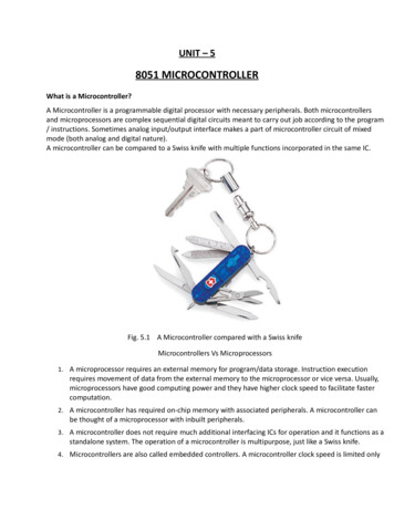
UNIT – 58051 MICROCONTROLLERWhat is a Microcontroller?A Microcontroller is a programmable digital processor with necessary peripherals. Both microcontrollersand microprocessors are complex sequential digital circuits meant to carry out job according to the program/ instructions. Sometimes analog input/output interface makes a part of microcontroller circuit of mixedmode (both analog and digital nature).A microcontroller can be compared to a Swiss knife with multiple functions incorporated in the same IC.Fig. 5.1 A Microcontroller compared with a Swiss knifeMicrocontrollers Vs Microprocessors1. A microprocessor requires an external memory for program/data storage. Instruction executionrequires movement of data from the external memory to the microprocessor or vice versa. Usually,microprocessors have good computing power and they have higher clock speed to facilitate fastercomputation.2. A microcontroller has required on-chip memory with associated peripherals. A microcontroller canbe thought of a microprocessor with inbuilt peripherals.3. A microcontroller does not require much additional interfacing ICs for operation and it functions as astandalone system. The operation of a microcontroller is multipurpose, just like a Swiss knife.4. Microcontrollers are also called embedded controllers. A microcontroller clock speed is limited only
to a few tens of MHz Microcontrollers are numerous and many of them are application specific.Development/Classification of microcontrollers (Invisible)Microcontrollers have gone through a silent evolution (invisible). The evolution can be rightly termed assilent as the impact or application of a microcontroller is not well known to a common user, althoughmicrocontroller technology has undergone significant change since early 1970's. Development of somepopular microcontrollers is given as follows.Intel 40044 bit (2300 PMOS trans, 108 kHz)1971Intel 80488 bit1976Intel 80318 bit (ROM-less).Intel 80518 bit (Mask ROM)1980Microchip PIC16C648 bit1985Motorola 68HC118 bit (on chip ADC).Intel 80C19616 bit1982Atmel AT89C518 bit (Flash memory).Microchip PIC 16F8778 bit (Flash memory ADC).Development of microprocessors (Visible)Microprocessors have undergone significant evolution over the past four decades. This development isclearly perceptible to a common user, especially, in terms of phenomenal growth in capabilities of personalcomputers. Development of some of the microprocessors can be given as follows.Intel 40044 bit (2300 PMOS transistors)1971Intel 808080858 bit (NMOS)8 bit1974Intel 8088808616 bit16 bit1978Intel 801868028616 bit16 bit1982
Intel 8038632 bit (275000 transistors)1985Intel 80486 SXDX32 bit32 bit (built in floating point unit)198964 bit19931997199920008 bit197632-bit1993Intel 80586IMMXCeleron IIIIIIVZ-80 (Zilog)Motorola Power PC6016026031995Some of the microcontrollers of 8051 family are given as Y16-BITNO. OFFULLTIMER/COUNTER VECTORED DUPLEX e26180511284k ROM25180522568k ROM36187511284k EPROM25187522568k EPROM361AT89C511284k Flash Memory251AT89C522568k Flash memory361
Various features of 8051 microcontroller are given as follows: 8-bit CPU 16-bit Program Counter 8-bit Processor Status Word (PSW) 8-bit Stack Pointer Internal RAM of 128bytes Special Function Registers (SFRs) of 128 bytes 32 I/O pins arranged as four 8-bit ports (P0 - P3) Two 16-bit timer/counters : T0 and T1 Two external and three internal vectored interrupts One full duplex serial I/OARCHITECTURE OF 8051 MICROCONTROLLER:It is 8-bit microcontroller, means MC 8051 can Read, Write and Process 8 bit data. This ismostly used microcontroller in the robotics, home appliances like mp3 player, washingmachines, electronic iron and industries. Mostly used blocks in the architecture of 8051 are asfollows:
1. Oscillator and clock generator:All operations in a microcontroller are synchronized by the help of an oscillator clock.The oscillator clock generates the clock pulses by which all internal operations are synchronized.A resonant network connected through pins XTAL1 and XTAL2 forms up an oscillator. For thispurpose a quartz crystal and capacitors are employed. The crystal run at specified maximumand minimum frequencies typically at 1 MHz to 16 MHz.
2. ALU:It is 8 bit unit. It performs arithmetic operation as addition, subtraction, multiplication,division, increment and decrement. It performs logical operations like AND, OR and EX-OR. Itmanipulates 8 bit and 16 bit data. It calculates address of jump locations in relative branchinstruction. It performs compare, rotate and compliment operations. It consists of Booleanprocessor which performs bit, set, test, clear and compliment. 8051 micro controller contains 34general purpose registers or working registers.2 of them are called math registers A & B and 32are bank of registers.a. Accumulator(A-reg):It is 8 bit register. Its address is E0H and it is bit and byte accessible. Result of arithmetic& logic operations performed by ALU is accumulated by this register. Therefore it is calledaccumulator register. It is used to store 8 bit data and to hold one of operand of ALU unitsduring arithmetical and logical operations. Most of the instructions are carried out onaccumulator data. It is most versatile of 2 CPU registers.b. B-register:It is special 8 bit math register. It is bit and byte accessible. It is used in conjunction withA register as I/P operand for ALU. It is used as general purpose register to store 8 bit data.c. PSW:It is 8 bit register. Its address is D0H and It is bit and byte accessible. It has 4 conditionalflags or math flags which sets or resets according to condition of result. It has 3 control flags, bysetting or resetting bit required operation or function can be achieved. The format of flagregister is as shown below:d. FLAG:1. Carry Flag(CY): During addition and subtraction any carry or borrow is generated thencarry flag is set otherwise carry flag resets. It is used in arithmetic, logical, jump, rotateand Boolean operations.2. Auxiliary carry flag(AC): If during addition and subtraction any carry or borrow isgenerated from lower 4 bit to higher 4 bit then AC sets else it resets. It is used in BCDarithmetic operations.3. Overflow flag(OV): If in signed arithmetic operations result exceeds more than 7 bitthan OV flag sets else resets.It is used in signed arithmetic operations only.4. Parity flag(P): If in result, even no. Of ones "1" are present than it is called even parityand parity flag sets. In result odd no. Of ones "1"are present than it is called odd parityand parity flag resets.ii. CONTROL FLAGS:1. FO: It is user defined flag. The user defines the function of this flag. The user can set,test n clear this flag through software.2. RS1 and RS0: These flags are used to select bank of register by resetting those flagswhich are as shown in table :
3. Program counter (PC): The Program Counter (PC) is a 2-byte address which tells the8051 where the next instruction to execute is found in memory. It is used to hold 16 bitaddress of internal RAM, external RAM or external ROM locations. When the 8051 isinitialized PC always starts at 0000h and is incremented each time an instruction isexecuted. It is important to note that PC isnt always incremented by one and neverdecremented.4. Data pointer register (DTPR): It is a 16 bit register used to hold address of external orinternal RAM where data is stored or result is to be stored. It is used to store 16 bit data.It is divided into2- 8bit registers, DPH-data pointer higher order (83H) and DPL-datapointer lower order (82H). Each register can be used as general purpose register to store8 bit data and can also be used as memory location. DPTR does not have single internaladdress. It functions as Base register in base relative addressing mode and in-directjump.5. Stack pointer (SP): It is 8-bit register. It is byte addressable. Its address is 81H. It isused to hold the internal RAM memory location addresses which are used as stackmemory. When the data is to be placed on stack by push instruction, the content ofstack pointer is incremented by 1, and when data is retrieved from stack, content ofstack of stack pointer is decremented by 1.iii. Special function Registers(SFR): The 8051 microcontroller has 11 SFR divided in 4 groups:A. Timer/Counter register: 8051 microcontroller has 2-16 bit Timer/counter registers calledTimer-reg-T0 And Timer/counter Reg-T1.Each register is 16 bit register divide into lower andhigher byte register as shown below: These register are used to hold initial no. of count. All ofthe 4 register are byte addressable.1. Timer control register: 8051 microcontroller has two 8-bit timer control register i.e.TMOD and TCON register. TMOD Register: it is 8-bit register. Its address is 89H. It is byteaddressable. It used to select mode and control operation of time by writing controlword.2. TCON register: It is 8-bit register. Its address is 88H. It is byte addressable. Its MSB 4bit are used to control operation of timer/ counter and LSB 4-bit are used for externalinterrupt control.B. Serial data register: 8051 micro controller has 2 serial data register viz. SBUF and SCON.1. Serial buffer register (SBUF): it is 8-bit register. It is byte addressable .Its address is99H. It is used to hold data which is to be transferred serially.2. Serial control register (SCON): it is 8-bit register. It is bit/byte addressable. Its addressis 98H. The 8-bit loaded into this register controls the operation of serial communication.C. Interrupt register: 8051 µC has 2 8-bit interrupt register.1. Interrupt enable register (IE): it is 8-bit register. It is bit/byte addressable. Its addressis A8H.it is used to enable and disable function of interrupt.2. Interrupt priority register (IP): It is 8-bit register. It is bit/byte addressable. Its addressis B8H. it is used to select low or high level priority of each individual interrupts.D. Power control register (PCON): it is 8-bit register. It is byte addressable .Its address is 87H. Itsbits are used to control mode of power saving circuit, either idle or power down mode and ion.
Internal RAMInternal RAM has memory 128-byte. See 8051 hardware for further internal RAM design.Internal RAM is organized into three distinct areas: 32 bytes working registers from address 00hto 1Fh 16 bytes bit addressable occupies RAM byte address 20h to 2Fh, altogether 128addressable bits General purpose RAM from 30h to 7Fh.Internal ROMData memory and program code memory both are in different physical memory butboth have the same addresses. An internal ROM occupied addresses from 0000h to 0FFFh. PCaddresses program codes from 0000h to 0FFFh. Program addresses higher than 0FFFh thatexceed the internal ROM capacity will cause 8051 architecture to fetch codes bytes fromexternal program memory.28 bytes of Internal RAM Structure (lower address space)Fig 5.3: Internal RAM StructureThe lower 32 bytes are divided into 4 separate banks. Each register bank has 8 registers of one byte each. Aregister bank is selected depending upon two bank select bits in the PSW register. Next 16bytes are bit
addressable. In total, 128bits (16X8) are available in bitaddressable area. Each bit can be accessed andmodified by suitable instructions. The bit addresses are from 00H (LSB of the first byte in 20H) to 7FH (MSBof the last byte in 2FH). Remaining 80bytes of RAM are available for general purpose.Internal Data Memory and Special Function Register (SFR) MapFig 5.4 : Internal Data Memory MapThe special function registers (SFRs) are mapped in the upper 128 bytes of internal data memory address.Hence there is an address overlap between the upper 128 bytes of data RAM and SFRs. Please note that theupper 128 bytes of data RAM are present only in the 8052 family. The lower128 bytes of RAM (00H - 7FH)can be accessed both by direct or indirect addressing while the upper 128 bytes of RAM (80H - FFH) areaccessed by indirect addressing.The SFRs (80H - FFH) are accessed by direct addressing only. This featuredistinguishes the upper 128 bytes of memory from the SFRs, as shown in fig 5.4.SFR MapThe set of Special Function Registers (SFRs) contains important registers such as Accumulator, Register B, I/OPort latch registers, Stack pointer, Data Pointer, Processor Status Word (PSW) and various control registers.Some of these registers are bit addressable (they are marked with a * in the diagram below). The detailedmap of various registers is shown in the following PSW*(T2CON)*IP*P3*(RCAP2L) (RCAP2H) (TL2)(TH2)
A8HA0H98H90H88H80HIE*P2*SCON*P1*TCON*P0*SBUFTMOD TL0SPDPLTL1DPHTH0TH1PCONFig 5.5: SFR MapIt should be noted hat all registers appearing in the first column are bit addressable. The bit address of a bitin the register is calculated as follows.Bit address of 'b' bit of register 'R' isAddress of register 'R' bwhere 0 b 7Processor Status Word (PSW)Address D0HFi g 5.6: Processor Status WordPSW register stores the important status conditions of the microcontroller. It also stores the bank select bits(RS1 & RS0) for register bank selection.Power saving modes of operation :8051 has two power saving modes. They are 1. Idle Mode2. Power Down mode.The two power saving modes are entered by setting two bits IDL and PD in the special function register(PCON) respectively.The structure of PCON register is as follows.PCON: Address 87HThe schematic diagram for 'Power down' mode and 'Idle' mode is given as follows:
Fig 12.2 Schematic diagram for Power Down and Idle mode implementationIdle ModeIdle mode is entered by setting IDL bit to 1 (i.e., 0). The clock signal is gated off to CPU, but not tothe interrupt, timer and serial port functions. The CPU status is preserved entirely. SP, PC, PSW,Accumulator and other registers maintain their data during IDLE mode. The port pins hold their logicalstates they had at the time Idle was initiated. ALE andare held at logic high levels.Ways to exit Idle Mode:1. Activation of any enabled interrupt will clear PCON.0 bit and hence the Idle Mode is exited. Theprogram goes to the Interrupt Service Routine (ISR). After RETI is executed at the end of the ISR,the next instruction will start from the one following the instruction that enabled Idle Mode.2. A hardware reset exits the idle mode. The CPU starts from the instruction following theinstruction that invoked the 'Idle' mode.Power Down Mode:The Power down Mode is entered by setting the PD bit to 1. The internal clock to the entiremicrocontroller is stopped (frozen). However, the program is not dead. The Power down Mode is exited(PCON.1 is cleared to 0) by Hardware Reset only. The CPU starts from the next instruction where thePower down Mode was invoked. Port values are not changed/ overwritten in power down mode. Vcccan be reduced to as low as 2V in Power Down mode. However, Vcc has to be restored to normal valuebefore Power Down mode is exited.MEMORY ORGANISATION:The 8051 has two types of memory and these are Program Memory and Data Memory. ProgramMemory (ROM) is used to permanently save the program being executed, while Data Memory (RAM) isused for temporarily storing data and intermediate results created and used during the operation ofthe microcontroller. Depending on the model in use (we are still talking about the 8051 microcontrollerfamily in general) at most a few Kb of ROM and 128 or 256 bytes of RAM is usedAll 8051 microcontrollers have a 16-bit addressing bus and are capable of addressing 64 kb memory. It
is neither a mistake nor a big ambition of engineers who were working on basic core development. It isa matter of smart memory organization which makes these microcontrollers a real “programmers’goody“.Program MemoryThe first models of the 8051 microcontroller family did not have internal program memory. It wasadded as an external separate chip. These models are recognizable by their label beginning with 803(for example 8031 or 8032). All later models have a few Kbyte ROM embedded. Even though such anamount of memory is sufficient for writing most of the programs, there are situations when it isnecessary to use additional memory as well. A typical example are so called lookup tables. They areused in cases when equations describing some processes are too complicated or when there is no timefor solving them. In such cases all necessary estimates and approximates are executed in advance andthe final results are put in the tables (similar to logarithmic tables).How does the microcontroller handle external memory depends on the EA pin logic state:
EA 0 In this case, the microcontroller completely ignores internal program memory and executes onlythe program stored in external memory.EA 1 In this case, the microcontroller executes first the program from built-in ROM, then the programstored in external memory.In both cases, P0 and P2 are not available for use since being used for data and address transmission.Besides, the ALE and PSEN pins are also used.Data MemoryAs already mentioned, Data Memory is used for temporarily storing data and intermediate resultscreated and used during the operation of the microcontroller. Besides, RAM memory built in the 8051family includes many registers such as hardware counters and timers, input/output ports, serial databuffers etc. The previous models had 256 RAM locations, while for the later models this number wasincremented by additional 128 registers. However, the first 256 memory locations (addresses 0-FFh) arethe heart of memory common to all the models belonging to the 8051 family. Locations available to theuser occupy memory space with addresses 0-7Fh, i.e. first 128 registers. This part of RAM is divided inseveral blocks.The first block consists of 4 banks each including 8 registers denoted by R0-R7. Prior to accessing any ofthese registers, it is necessary to select the bank containing it. The next memory block (address 20h2Fh) is bit- addressable, which means that each bit has its own address (0-7Fh). Since there are 16 suchregisters, this block contains in total of 128 bits with separate addresses (address of bit 0 of the 20h
byte is 0, while address of bit 7 of the 2Fh byte is 7Fh). The third group of registers occupy addresses2Fh-7Fh, i.e. 80 locations, and does not have any special functions or features.Additional RAMIn order to satisfy the programmers’ constant hunger for Data Memory, the manufacturers decided toembed an additional memory block of 128 locations into the latest versions of the 8051microcontrollers. However, it’s not as simple as it seems to be The problem is that electronicsperforming addressing has 1 byte (8 bits) on disposal and is capable of reaching only the first 256locations, therefore. In order to keep already existing 8-bit architecture and compatibility with otherexisting models a small trick was done.What does it mean? It means that additional memory block shares the same addresses with locationsintended for the SFRs (80h- FFh). In order to differentiate between these two physically separatedmemory spaces, different ways of addressing are used. The SFRs memory locations are accessed bydirect addressing, while additional RAM memory locations are accessed by indirect addressing.
Memory expansionIn case memory (RAM or ROM) built in the microcontroller is not sufficient, it is possible to add twoexternal memory chips with capacity of 64Kb each. P2 and P3 I/O ports are used for their addressingand data transmission.
From the user’s point of view, everything works quite simply when properly connected because mostoperations are performed by the microcontroller itself. The 8051 microcontroller has two pins for dataread RD#(P3.7) and PSEN#. The first one is used for reading data from external data memory (RAM),while the other is used for reading data from external program memory (ROM). Both pins are activelow. A typical example of memory expansion by adding RAM and ROM chips (Hardward architecture), isshown in figure above.Even though additional memory is rarely used with the latest versions of the microcontrollers, we willdescribe in short what happens when memory chips are connected according to the previousschematic. The whole process described below is performed automatically.When the program during execution encounters an instruction which resides in external memory(ROM), the microcontroller will activate its control output ALE and set the first 8 bits of address (A0-A7)on P0. IC circuit 74HCT573 passes the first 8 bits to memory address pins.A signal on the ALE pin latches the IC circuit 74HCT573 and immediately afterwards 8 higher bits ofaddress (A8-A15) appear on the port. In this way, a desired location of additional program memory isaddressed. It is left over to read its content.
Port P0 pins are configured as inputs, the PSEN pin is activated and the microcontroller reads frommemory chip.Similar occurs when it is necessary to read location from external RAM. Addressing is performed in thesame way, while read and write are performed via signals appearing on the control outputs RD (is shortfor read) or WR (is short for write).Interfacing External MemoryIf external program/data memory are to be interfaced, they are interfaced in the following way.Fig 6.1: Circuit Diagram for Interfacing of External MemoryExternal program memory is fetched if either of the following two conditions are satisfied.1.(Enable Address) is low. The microcontroller by default starts searching for program fromexternal program memory.2. PC is higher than FFFH for 8051 or 1FFFH for 8052.tells the outside world whether the external memory fetched is program memory or data memory.
is user configurable.is processor controlled.8051 INSTRUCTION SET AND PROGRAMMING:8051 Addressing Modes8051 has four addressing modes.1. Immediate Addressing: Data is immediately available in the instruction.For example ADD A, #77; Adds 77 (decimal) to A and stores in AADD A, #4DH; Adds 4D (hexadecimal) to A and stores in AMOV DPTR, #1000H; Moves 1000 (hexadecimal) to data pointer2. Register Addressing: This way of addressing accesses the bytes in the current register bank. Data isavailable in the register specified in the instruction. The register bank is decided by 2 bits of ProcessorStatus Word (PSW).For exampleADD A, R0; Adds content of R0 to A and stores in A3. Direct Addressing: The address of the data is available in the instruction.For example MOV A, 088H; Moves content of SFR TCON (address 088H)to A4. Register Indirect Addressing: The address of data is available in the R0 or R1 registers as specified in theinstruction.For example MOV A, @R0 moves content of address pointed by R0 to AExternal Data Addressing:Pointer used for external data addressing can be either R0/R1 (256 byte access) or DPTR (64kbyte access).For example MOVX A, @R0; Moves content of 8-bit address pointed by R0 to AMOVX A, @DPTR; Moves content of 16-bit address pointed by DPTR to AExternal Code Addressing:Sometimes we may want to store non-volatile data into the ROM e.g. look-up tables. Such data may requirereading the code memory. This may be done as follows MOVC A, @A DPTR; Moves content of address pointed by A DPTR to AMOVC A, @A PC; Moves content of address pointed by A PC to A
INSTRUCTION SET OF 8051:The C8051 instructions are divided into five functional groups:1. Arithmetic operations2. Logical operations3. Data transfer operations4. Boolean variable operations5. Program branching operationArithmetic Operations:OPCODEOPERANDDESCRIPTIONNO. OF BYTESADDA,RnAdd register to Accumulator1ADDA,directAdd direct byte to Accumulator2ADDA,@RiAdd indirect RAM to Accumulator1ADDA,#dataAdd immediate data to Accumulator2ADDCA,RnAdd register to Accumulator with Carry1ADDCA,directAdd direct byte to Accumulator with Carry2ADDCA,@RiAdd indirect RAM to Accumulator with Carry 1ADDCA,#dataAdd immediate data to Acc with Carry2SUBBA,RnSubtract Register from Acc with borrow1SUBBA,directSubtract direct byte from Acc with borrow2SUBBA,@RiSubtract indirect RAM from ACC with borrow 1SUBBA,#dataSubtract immediate data from Acc withborrow2INCAIncrement Accumulator1INCRnIncrement register1
Each port of 8051 has bidirectional capability. Port 0 is called 'true bidirectional port' as it floats (tristated)when configured as input. Port-1, 2, 3 are called 'quasi bidirectional port'.Port-0 Pin StructurePort -0 has 8 pins (P0.0-P0.7).The structure of a Port-0 pin is shown in fig 6.2.Fig 6.2: Port-0 StructurePort-0 can be configured as a normal bidirectional I/O port or it can be used for address/data interfacing foraccessing external memory. When control is '1', the port is used for address/data interfacing. When thecontrol is '0', the port can be used as a normal bidirectional I/O port.Let us assume that control is '0'. When the port is used as an input port, '1' is written to the latch. In thissituation both the output MOSFETs are 'off'. Hence the output pin floats. This high impedance pin can bepulled up or low by an external source. When the port is used as an output port, a '1' written to the latchagain turns 'off' both the output MOSFETs and causes the output pin to float. An external pull-up is requiredto output a '1'. But when '0' is written to the latch, the pin is pulled down by the lower MOSFET. Hence theoutput becomes zero.When the control is '1', address/data bus controls the output driver MOSFETs. If the address/data bus(internal) is '0', the upper MOSFET is 'off' and the lower MOSFET is 'on'. The output becomes '0'. If theaddress/data bus is '1', the upper transistor is 'on' and the lower transistor is 'off'. Hence the output is '1'.Hence for normal address/data interfacing (for external memory access) no pull-up resistors are required.Port-0 latch is written to with 1's when used for external memory access.Port-1 Pin Structure
Port-1 has 8 pins (P1.1-P1.7) .The structure of a port-1 pin is shown in fig 6.3.Fig 6.3 Port 1 StructurePort-1 does not have any alternate function i.e. it is dedicated solely for I/O interfacing. When used asoutput port, the pin is pulled up or down through internal pull-up. To use port-1 as input port, '1' has to bewritten to the latch. In this input mode when '1' is written to the pin by the external device then it read fine.But when '0' is written to the pin by the external device then the external source must sink current due tointernal pull-up. If the external device is not able to sink the current the pin voltage may rise, leading to apossible wrong reading.PORT 2 Pin StructurePort-2 has 8-pins (P2.0-P2.7) . The structure of a port-2 pin is shown in fig 6.4.Fig 6.4 Port 2 Structure
Port-2 is used for higher external address byte or a normal input/output port. The I/O operation is similar toPort-1. Port-2 latch remains stable when Port-2 pin are used for external memory access. Here again due tointernal pull-up there is limited current driving capability.PORT 3 Pin StructurePort-3 has 8 pin (P3.0-P3.7) . Port-3 pins have alternate functions. The structure of a port-3 pin is shown infig 6.5.Fig 6.5 Port 3 StructureEach pin of Port-3 can be individually programmed for I/O operation or for alternate function. The alternatefunction can be activated only if the corresponding latch has been written to '1'. To use the port as inputport, '1' should be written to the latch. This port also has internal pull-up and limited current drivingcapability.Alternate functions of Port-3 pins are P3.0RxDP3.1TxDP3.2P3.3P3.4T0
P3.5T1P3.6P3.7Note:1. Port 1, 2, 3 each can drive 4 LS TTL inputs.2. Port-0 can drive 8 LS TTL inputs in address /data mode. For digital output port, it needs external pull-up resistors.3. Ports-1,2and 3 pins can also be driven by open-collector or open-drain outputs.4. Each Port 3 bit can be configured either as a normal I/O or as a special function bit.Reading a port (port-pins) versus reading a latchThere is a subtle difference between reading a latch and reading the output port pin.The status of the output port pin is sometimes dependant on the connected load. For instance if a port isconfigured as an output port and a '1' is written to the latch, the output pin should also show '1'. If theoutput is used to drive the base of a transistor, the transistor turns 'on'.If the port pin is read, the value will be '0' which is corresponding to the base-emitter voltage of thetransistor.Reading a latch: Usually the instructions that read the latch, read a value, possibly change it, and thenrewrite it to the latch. These are called "read-modify-write" instructions. Examples of a few instructions areORL P2, A; P2 -- P2 or AMOV P2.1, C; Move carry bit to PX.Y bit.In this the latch value of P2 is read, is modified such that P2.1 is the same as Carry and is then written backto P2 latch.Reading a Pin: Examples of a few instructions that read port pin, areMOV A, P0 ; Move port-0 pin values to AMOV A, P1; Move port-1 pin values to AINTERRUPTS OF 8051:
There are five interrupt sources for the 8051, which means that they can recognize 5 differentevents that can interrupt regular program execution. Each interrupt can be enabled or disabledby setting bits of the IE register. Likewise, the whole interrupt system can be disabled by clearingthe EA bit of the same register. Refer to figure below.Now, it is necessary to explain a few details referring to external interrupts- INT0 and INT1. Ifthe IT0 and IT1 bits of the TCON register are set, an interrupt will be generated on high to lowtransition, i.e. on the falling pulse edge (only in that moment). If these bits are cleared, aninterrupt will be continuously executed as far as the pins are held low.IE Register (Interrupt Enable) EA – global interrupt enable/disable:o0 – disables all interrupt requests.o1 – enables all
clearly perceptible to a common user, especially, in terms of phenomenal growth in capabilities of personal computers. Development of some of the microprocessors can be given as follows. Intel 4004 4 bit (2300 PMOS transistors) 1971 Intel 8080 8085 8 bit (NMOS) 8 bit 1974 Intel 8088 8086 16 bit 16 bit 1978 Intel 80186 80286 16 bit 16 bit 1982