Transcription
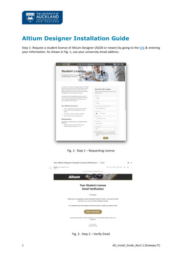
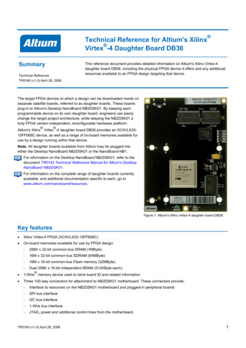
Technical Reference for Altium's Xilinx Virtex -4 Daughter Board DB36Summary This reference document provides detailed information on Altium's Xilinx Virtex-4daughter board DB36, including the physical FPGA device it offers and any additionalresources available to an FPGA design targeting that device.Technical ReferenceTR0160 (v1.0) April 28, 2008The target FPGA devices to which a design can be downloaded reside onseparate satellite boards, referred to as daughter boards. These boardsplug-in to Altium's Desktop NanoBoard NB2DSK01. By keeping eachprogrammable device on its own daughter board, engineers can easilychange the target project architecture, while keeping the NB2DSK01 atruly FPGA vendor-independent, reconfigurable hardware platform. Altium's Xilinx Virtex -4 daughter board DB36 provides an XC4VLX2510FF668C device, as well as a range of on-board memories available foruse by a design running within that device.Note: All daughter boards available from Altium may be plugged intoeither the Desktop NanoBoard NB2DSK01 or the NanoBoard-NB1.For information on the Desktop NanoBoard NB2DSK01, refer to thedocument TR0143 Technical Reference Manual for Altium's DesktopNanoBoard NB2DSK01.For information on the complete range of daughter boards currentlyavailable, and additional documentation specific to each, go towww.altium.com/nanoboard/resources.Figure 1. Altium's Xilinx Virtex-4 daughter board DB36.Key features Xilinx Virtex-4 FPGA (XC4VLX25-10FF668C) On-board memories available for use by FPGA design:-256K x 32-bit common-bus SRAM (1MByte)-16M x 32-bit common-bus SDRAM (64MByte)-16M x 16-bit common-bus Flash memory (32MByte)-Dual 256K x 16-bit independent SRAM (512KByte each) 1-Wire memory device used to store board ID and related information Three 100-way connectors for attachment to NB2DSK01 motherboard. These connectors provide:-Interface to resources on the NB2DSK01 motherboard and plugged-in peripheral boards-SPI bus interface-I2C bus interface-1-Wire bus interface-JTAG, power and additional control lines from the motherboard.TR0160 (v1.0) April 28, 20081
Technical Reference for Altium's Xilinx Virtex-4 Daughter Board DB36Functional overviewDB36 - Xilinx Virtex-4 Daughter BoardNB2DSK01 Motherboard1-Wire Bus1-WireMemoryNanoTalk ControllerCommon-BusSRAMMotherboardResources Accessibleby FPGA Design(e.g. TFT LCD panel,CAN, RS-232)Common-BusSDRAMXilinx Virtex-4XC4VLX25-10FF668CCommon-BusFlash MemoryPeripheral Board A1-Wire BusPeripheral Board BIndependent SRAMPeripheral Board rSupplies5V5VFigure 2. Xilinx Virtex-4 daughter board (DB36) block diagram.3-connector daughter boardDaughter boards available with the Desktop NanoBoard NB2DSK01 and beyond each have three connectors (top, bottom andleft). These are referred to as '3-connector' daughter boards. Those available previously for the NanoBoard-NB1 have two suchconnectors (top and bottom) and are referred to as '2-connector' daughter boards. The Xilinx Virtex-4 daughter board (DB36) isa 3-connector daughter board.3-connector daughter boards also have three holes that align with threaded standoffs on the NB2DSK01. These can be used toaffix the board securely to the motherboard.2TR0160 (v1.0) April 28, 2008
Technical Reference for Altium's Xilinx Virtex-4 Daughter Board DB36Attachment to the NB2DSK01 motherboardThe daughter board is mounted onto the NB2DSK01motherboard by plugging its three 100-way Male dockingconnectors into the motherboard's corresponding three 100way Female docking connectors – designated HDR T1,HDR L1 and HDR B1. These are referred to as'NANOCONNECT' interfaces. The board can be securelyfixed in place using the available threaded standoffs.Accessing motherboard resourcesThe daughter board connectors on the motherboard map I/Oresources on the NB2DSK01 directly to the pins of thedaughter board FPGA device, as if that device weremounted directly on the motherboard.For more information on the NB2DSK01 motherboardresources made available to a daughter board FPGAdevice, see the section Resources accessible from anFPGA design, in the document TR0143 TechnicalReference Manual for Altium's Desktop NanoBoardNB2DSK01.Figure 3. Daughter board connectors on the NB2DSK01 motherboard –the docking point for a satellite daughter board.Accessing peripheral board resourcesResources on the plug-in peripheral boards are also made available to the daughter board FPGA device. The corresponding I/Opins from each peripheral board connector – 50 each – are wired directly to pins of the daughter board connectors on themotherboard: Peripheral Board A and B connector signals are wired to daughter board connector HDR L1 Peripheral Board C connector signals are wired to daughter board connector HDR T1These signals are subsequently wired to I/O pins of the daughter board's FPGA device. By keeping the signals generic – basedon the peripheral board connector position and not on the resources – the peripheral boards can be attached to the NB2DSK01in any of the three peripheral board positions.Note: Some peripheral boards (e.g. PB01 – the Audio / Video Peripheral Board) are twice the width of other available peripheralboards and, as such, can only be connected to the NB2DSK01 using the 'PERIPHERAL BOARD A' or 'PERIPHERAL BOARDC' connectors.For more information on peripheral boards, see the section Peripheral Boards, in the document TR0143 TechnicalReference Manual for Altium's Desktop NanoBoard NB2DSK01. For information on the range of peripheral boards currentlyavailable and additional documentation specific to each, go to www.altium.com/nanoboard/resources.Additional servicesIn addition to the user-available I/O on the motherboard and peripheral boards, the daughter board connectors provide pins for aseries of other functions, including implementation of the NanoTalk communications protocol, power, and programming of theFPGA device. The following sections detail these additional signals, in relation to the daughter board connectors on thedaughter board itself.Hard JTAG signalsAll daughter board devices that are JTAG-equipped are connected to signals FPGA TMS, FPGA TCK, FPGA TDI andFPGA TDO. This allows the NB2DSK01 and Altium Designer to address the daughter board hardware using the JTAG protocol.Soft JTAG signalsFour FPGA I/O pins are reserved for JTAG signals that are utilized by the FPGA design. Altium Designer uses JTAG IP tocommunicate directly with the FPGA fabric, allowing applications to be debugged live. These signals (NEXUS TMS, NEXUS TCK,NEXUS TDI and NEXUS TDO) are derived in the NB2DSK01's NanoTalk Controller, which is implemented in a Xilinx Spartan-3on the motherboard.For more information on the JTAG communications, refer to the article AR0130 PC to NanoBoard Communications.TR0160 (v1.0) April 28, 20083
Technical Reference for Altium's Xilinx Virtex-4 Daughter Board DB36Daughter board identification signalsFPGA devices from different manufacturers and families require differing auto-configuration processes, so it is necessary for theNanoTalk Controller to be able to identify the device family.Board identification is achieved through use of a 1-Wire slave memory device located on the daughter board. This devicecarries more than enough storage capacity to hold information such as Board ID, physical Device ID, board revision, and so on.For more information, see the section Board ID memory later in this document.To satisfy NanoBoard-NB1 compatibility requirements, four signals (FPGA ID0.FPGA ID3) are hardwired on the daughterboard to provide the required identification to the NanoTalk Controller. For the Xilinx Virtex-4 daughter board (DB36), these foursignals are tied to GND, giving an FPGA ID value of 0h.SPI bus interfaceThe NB2DSK01 SPI system involves a variety of SPI-compatible slave resources, located across the hardware system – on theNB2DSK01 motherboard itself and also on certain peripheral boards that plug in to the motherboard. These SPI resources areaccessible by three distinct SPI masters: Altium Designer (via the parallel or USB connection) The firmware – more specifically a TSK3000A processor therein – loaded onto the motherboard's Spartan-3 FPGA device(the NanoTalk Controller) The design loaded onto the currently plugged-in daughter board FPGA device.Providing the required SPI bus arbitration between the masters, and access to the SPI devices, is the NB2DSK01's SPIController. The Controller, which is part of the NanoBoard firmware, plays the role of multiplexer/router – determining whichmaster has access to the SPI bus and which SPI slave device is selected for communications.From an FPGA design perspective, the NB2DSK01's SPI Controller provides an SPI path from the daughter board to each ofthe SPI slave resources resident in the system.Daughter board connector signals SPI DIN, SPI DOUT, SPI CLK, SPI SEL and SPI MODE provide the required connectivityfrom the daughter board. During operation, the daughter board FPGA design communicates with the NB2DSK01's SPIController to establish a path between the design and a specific motherboard/peripheral board SPI device.For detailed information on the Desktop NanoBoard's SPI communications system, refer to the document AP0163 SPICommunications on the Desktop NanoBoard NB2DSK01. 1-Wire bus interfaceA 1-Wire serial bus interface signal is provided (ONE WIRE DB PB) which is connected through to each of the NB2DSK01'speripheral board connectors. This provides the ability to communicate directly from a processor in an FPGA design, with one ormore slave 1-Wire compatible devices located across plugged-in peripheral boards (where such devices exist). As the 1-Wirebus is made available to all three peripheral board sites it allows development of a dedicated network of 1-Wire devices – amicro-LAN if you will.Daughter board power signalsDaughter board connectors HDR T and HDR B provide two power supplies to the daughter board, as well as ground signals.The power supply voltages – sourced from the NB2DSK01 motherboard – are 5V and 3.3V.Note: The maximum current available to the daughter board will depend upon the number and type of peripheral boardsattached to the motherboard, as well as the power requirements of each individual rail. In any case, the total connector contactrating of 2.0A for both the 3.3V and 5V rails is not to be exceeded. The maximum return ground current for all rails should notexceed 3A.Daughter board FPGA control signalsDaughter board connector HDR T handles various signals between the NanoTalk Controller and the daughter board FPGAdevice, that are used to control that device. Such signals include detection of an FPGA device when a daughter board isplugged-in to the motherboard, as well as signals used to actually program the device with an FPGA design.4TR0160 (v1.0) April 28, 2008
Technical Reference for Altium's Xilinx Virtex-4 Daughter Board DB36A word about changing daughter boardsWhen changing FPGA daughter boards, please take care not to damagethe connectors that attach the daughter board to the NB2DSK01. Thefollowing procedure is recommended:1. Ensure that the NB2DSK01's power is switched off.2. If using a 3-connector daughter board, ensure that any screws affixingit to the motherboard are removed.3. Grip the two sides of the daughter board between your thumb andfingers and gently pull the daughter board upwards. Gently rockingthe daughter board from side to side can help loosen the connectors.4. As the daughter board disengages, ensure that you keep the boardparallel to the motherboard and pull it straight up until all connectorsare fully disengaged.5. Install a different daughter board by gently positioning it so that itsconnectors are aligned with the corresponding connectors on themotherboard – the posts of which slot through the holes in thedaughter board.Figure 4. Switch daughter boards to change the targetarchitecture.If using a 2-connector daughter board, place its locator 'legs' into thecorresponding holes in the motherboard.Once located, press the daughter board firmly onto the NanoBoard. If using a 3-connector daughter board, such as the XilinxVirtex-4 daughter board (DB36), you can secure it to the motherboard using the available threaded standoffs.6. Switch the NB2DSK01's power on.The system software interrogates the NB2DSK01 at regular intervals to determine the FPGA device installed. If you changedaughter boards, the system will automatically detect the change and show the correct device in the Devices view. When theDevices view is active you can force the system to poll the NB2DSK01 by pressing the F5 key.TR0160 (v1.0) April 28, 20085
Technical Reference for Altium's Xilinx Virtex-4 Daughter Board DB36Daughter board resourcesThe resources on the Xilinx Virtex-4 daughter board (DB36) can be divided into the following key areas: General board resources – including connectors, power supplies and LEDs Target FPGA device – the primary element of the board, into which an FPGA design is programmed User resources – resources made available for use by the FPGA design itself, such as memory storage devices.The following sections take a closer look at these three areas.Note: For each of the following resources, reference is made to the corresponding sheet(s) of the daughter board schematicson which the circuitry of interest can be found. A pdf document of these schematics – DB36 Xilinx Virtex-4 (XC4VLX25-FF668)Daughter Board Schematics.pdf – can be found at www.altium.com/nanoboard/resources.General board resourcesThe following is a list of general resources found on the DB36.Docking connectorsThe DB36 is a 3-connector daughter board and, as such, has three 100way Male connectors. These are used to connect the daughter board tothe NB2DSK01 motherboard, which has corresponding 100-way Femaleconnectors ('NANOCONNECT'interfaces).The connectors on the daughter board are designated HDR T, HDR L andHDR BNote: HDR T and HDR B connectors are wired such that the daughterboard may be attached to either the Desktop NanoBoard NB2DSK01 orthe NanoBoard-NB1.Location on boardThe docking connectors (HDR T, HDR L and HDR B) are located on thesolder side of the board.Figure 5. Docking connectors on the daughter board,used to attach the board to the NB2DSK01 motherboard.Schematic referenceThe docking connectors can be found on sheetDB MotherBoardConnectors.SchDoc (entitled NB2 to Daughter Board Connectors) of the daughter board schematics.Board ID memoryBoard identification is handled courtesy of a DS2406 device (from Dallas Semiconductor).Although the device is actually a dual-addressable switch, it is used for the additional 1kbit ofmemory that it possesses. The DS2406 is a 1-Wire compatible device, primarily used to contain a code with which toidentify the daughter board when plugged in. The NanoTalk Controller interrogates this deviceover a single wire, the associated signal of which arrives at the Controller as ONE WIRE DBID.The DS2406 supports half-duplex communication at a rate of up to 16.3kbits/s. Although powerfor the device is sourced over the same single wire as the data itself – courtesy of a parasiticcapacitor which charges when the 1-Wire bus signal line is High – the device is also fed fromthe daughter board's 3.3V supply, to ensure continuous power.Similar devices on all peripheral boards and 3-connector daughter boards allow the NanoTalkController to detect which specific boards are available to the system.Figure 6. 1-Wire memory used tocontain the ident code for theboard.Location on boardThe DS2406 device (designated U1 ID) is located on the solder side of the board, to the top-left of the 100-way dockingconnector HDR T.Schematic referenceThe 1-Wire memory device can be found on sheet 1WB DS2406 EPROM.SchDoc (entitled 1-Wire Bus ID) of the daughterboard schematics.6TR0160 (v1.0) April 28, 2008
Technical Reference for Altium's Xilinx Virtex-4 Daughter Board DB36Further device informationFor more information on the DS2406 device, refer to the datasheet (DS2406.pdf) available at www.maxim-ic.com.PowerIn addition to the 3.3V and 5V supply voltages and ground signals fed to the daughter boardfrom the NB2DSK01 motherboard, the daughter board also has its own 1.2V and 2.5Vsupplies.The 1.2V supply is generated by passing the regulated 5V supply through a low-voltage stepdown regulator – a MAX1831 device, from Maxim.The 2.5V supply is sourced from the output of an adjustable linear voltage regulator – aMAX8860 device, from Maxim. Powered by the DB36's 5V supply, the output level isdetermined by the resistance between the device's OUT and SET pins, and is calculatedusing the following formula:VOUT 1.25 * (1 RA/100K)Figure 7. MAX1831 (U2) device.Where,VOUT is the voltage output of the deviceRA is the resistance between the device's OUT and SET pins.On the DB36, a resistance of 100K is used, giving a nominal analog power supply of 2.5V.The daughter board provides an array of test points for checking the integrity of each of the board's power supplies, as well asGND.Location on boardThe MAX1831 device (designated U2) is located on the component side of the board, to the right of the Xilinx Virtex-4 device.The MAX8860 device (designated U11) is located on the solder side of the board.The power supply test points (designated TP0 – TP4) are located on the component side of the board, to the right of the Flashmemory device (U1 CM).Schematic referenceThe power supply-related circuitry can be found on the following sheets of the daughter boardschematics. PSU.SchDoc (entitled Power Supply Top Level) PSU MAX1831 1V2 ALT.SchDoc (entitled Power Supply MAX1831 (1V2)) PSU MAX8860 ADJ.SchDoc (entitled Power Supply MAX8860 (2V5))Further device informationFor more information on the MAX1831 and MAX8860 devices, refer to the datasheets (MAX1830MAX1831.pdf and MAX8860.pdf) available at www.maxim-ic.com.Figure 8. Power supplytest points.Power and Program LEDsThe daughter board provides the following two LEDs: Power LED – this will light (RED) when the daughter board is correctly plugged intothe motherboard and the NB2DSK01's power is switched on. It signifies presence ofthe 3.3V supply to the board.Figure 9. Power and Program LEDs.Program LED – this will light (GREEN) when the target device on the daughter boardhas been successfully programmed with an FPGA design.Location on boardThe two LEDs, labeled 'POWER'(LED1) and 'PROGRAM'(LED2) respectively, are located at the bottom of the board, on thecomponent side.Schematic referenceThe LEDs can be found on sheet DB LEDS.SchDoc (entitled Daughter Board LEDs) of the daughter board schematics.TR0160 (v1.0) April 28, 20087
Technical Reference for Altium's Xilinx Virtex-4 Daughter Board DB36Target FPGA deviceThe XC4VLX25-10FF668C device on the daughter board is a member of the Virtex-4 family ofFPGAs. The Virtex-4 family is comprised of 17 devices in total, over three platform families – LX,SX and FX. The LX series, of which the daughter board device is a member, provide a highperformance solution for logic applications.The Virtex-4 family provides devices offering densities ranging from 12,312 to 200,448 LogicCells. The XC4VLX25-10FF668C offers 24,192 Logic Cells. Table 1 provides an informationsummary for this device.Note: In order to use the Virtex-4 device on this daughter board, you will need to install the relevant Vendor tools – Xilinx ISE or Xilinx ISE WebPACK from www.xilinx.com.Figure 10. Xilinx Virtex-4 FPGA(XC4VLX25-10FF668C).Table 1. Feature summary for the Virtex-4 FPGA device.FeatureDescriptionDevice kage668-Ball Flip Chip Fine Pitch Ball Grid Array (FF668)Speed Grade10 (Lowest)Temperature GradeCommercialPin Count668Total I/O Banks11Maximum User I/O Pins448Max. Differential I/O Pairs224Max. High-Speed Differential I/O Pairs0Xilinx Logic Cells24,192CLB Array2,688 CLBs (96 rows by 28 columns). (1 CLB 4 Slices, giving 10,752 Slices).Embedded (Block) RAM1296K bits (72 dual-port RAM blocks, each 18K bits)Distributed RAM168K bitsEmbedded Multipliers (18x18)48 (each 18x18 multiplier is part of an XtremeDSP slice, which also includesan accumulator and an adder/subtracter).Digital Clock Managers (DCM)8Phase Matched Clock Dividers (PMCD)4Global Clock Resources32Configuration Memory Required8,037,312 bitsOn-Chip Termination SupportYes8TR0160 (v1.0) April 28, 2008
Technical Reference for Altium's Xilinx Virtex-4 Daughter Board DB36Supported single-ended I/O standardsTable 2 lists the single-ended I/O standards supported by the XC4VLX25-10FF668C device.Table 2. Supported single-ended I/O standards.I/O StandardDescriptionGTLGunning Transceiver LogicGTLPGunning Transceiver Logic PlusHSTL IHigh-Speed Transceiver Logic (1.5V) Class IHSTL IIHigh-Speed Transceiver Logic (1.5V) Class IIHSTL IIIHigh-Speed Transceiver Logic (1.5V) Class IIIHSTL IVHigh-Speed Transceiver Logic (1.5V) Class IVHSTL I 18High-Speed Transceiver Logic (1.8V) Class IHSTL II 18High-Speed Transceiver Logic (1.8V) Class IIHSTL III 18High-Speed Transceiver Logic (1.8V) Class IIIHSTL IV 18High-Speed Transceiver Logic (1.8V) Class IVLVCMOS15Low-Voltage Complementary Metal-Oxide Semiconductor (1.5V)LVCMOS18Low-Voltage Complementary Metal-Oxide Semiconductor (1.8V)LVCMOS25Low-Voltage Complementary Metal-Oxide Semiconductor (2.5V)LVCMOS33Low-Voltage Complementary Metal-Oxide Semiconductor (3.3V)LVTTLLow-Voltage Transistor-Transistor Logic (3.3V)PCI33 3Peripheral Component Interconnect (33MHz, 3.3V)PCI66 3Peripheral Component Interconnect (66MHz, 3.3V)PCIXPeripheral Component Interconnect Extended (133MHz, 3.3V)SSTL18 IStub Series Terminated Logic (1.8V) Class ISSTL18 IIStub Series Terminated Logic (1.8V) Class IISSTL2 IStub Series Terminated Logic (2.5V) Class ISSTL2 IIStub Series Terminated Logic (2.5V) Class IISupported differential I/O standardsTable 3 lists the differential I/O standards supported by the XC4VLX25-10FF668C device.Table 3. Supported differential I/O standards.I/O StandardDescriptionBLVDS 25Bus Low-Voltage Differential Signaling (2.5V)DIFF HSTL IIDifferential High-Speed Transceiver Logic (1.5V) Class IIDIFF HSTL II 18Differential High-Speed Transceiver Logic (1.8V) Class IIDIFF SSTL18 IIDifferential Stub Series Terminated Logic (1.8V) Class IIDIFF SSTL2 IIDifferential Stub Series Terminated Logic (2.5V) Class IILDT 25Lightning Data Transport (2.5V) – also referred to as Hypertransport LVDS 25Low-Voltage Differential Signaling (2.5V)TR0160 (v1.0) April 28, 20089
Technical Reference for Altium's Xilinx Virtex-4 Daughter Board DB36LVDSEXT 25Extended Low-Voltage Differential Signaling (2.5V)LVPECL 25Low-Voltage Positive Emitter-Coupled Logic (2.5V)RSDS 25Reduced Swing Differential Signaling (2.5V)ULVDS 25Ultra Low-Voltage Differential Signaling with Differential Termination (2.5V)Supported single-ended DCI I/O standardsTable 4 lists the single-ended DCI (Digitally Controlled Impedance) I/O standards supported by the XC4VLX25-10FF668Cdevice.Table 4. Supported single-ended DCI I/O standards.I/O StandardDescriptionGTL DCIGunning Transceiver Logic with Digitally Controlled Impedance technologyGTLP DCIGunning Transceiver Logic Plus with Digitally Controlled Impedance technologyHSLVDCI 15High-Speed Low-Voltage Complementary Metal-Oxide Semiconductor (1.5V) with Digitally ControlledImpedance technologyHSLVDCI 18High-Speed Low-Voltage Complementary Metal-Oxide Semiconductor (1.8V) with Digitally ControlledImpedance technologyHSLVDCI 25High-Speed Low-Voltage Complementary Metal-Oxide Semiconductor (2.5V) with Digitally ControlledImpedance technologyHSLVDCI 33High-Speed Low-Voltage Complementary Metal-Oxide Semiconductor (3.3V) with Digitally ControlledImpedance technologyHSTL I DCIHigh-Speed Transceiver Logic (1.5V) Class I with Digitally Controlled Impedance technologyHSTL II DCIHigh-Speed Transceiver Logic (1.5V) Class II with Digitally Controlled Impedance technologyHSTL III DCIHigh-Speed Transceiver Logic (1.5V) Class III with Digitally Controlled Impedance technologyHSTL IV DCIHigh-Speed Transceiver Logic (1.5V) Class IV with Digitally Controlled Impedance technologyHSTL I 18 DCIHigh-Speed Transceiver Logic (1.8V) Class I with Digitally Controlled Impedance technologyHSTL II 18 DCIHigh-Speed Transceiver Logic (1.8V) Class II with Digitally Controlled Impedance technologyHSTL III 18 DCIHigh-Speed Transceiver Logic (1.8V) Class III with Digitally Controlled Impedance technologyHSTL IV 18 DCIHigh-Speed Transceiver Logic (1.8V) Class IV with Digitally Controlled Impedance technologyLVDCI 15Low-Voltage Complementary Metal-Oxide Semiconductor (1.5V) with Digitally Controlled ImpedancetechnologyLVDCI 18Low-Voltage Complementary Metal-Oxide Semiconductor (1.8V) with Digitally Controlled ImpedancetechnologyLVDCI 25Low-Voltage Complementary Metal-Oxide Semiconductor (2.5V) with Digitally Controlled ImpedancetechnologyLVDCI 33Low-Voltage Complementary Metal-Oxide Semiconductor (3.3V) with Digitally Controlled ImpedancetechnologyLVDCI DV2 15Low-Voltage Complementary Metal-Oxide Semiconductor (1.5V) with Digitally Controlled Impedancetechnology supporting controlled impedance drivers with half impedanceLVDCI DV2 18Low-Voltage Complementary Metal-Oxide Semiconductor (1.8V) with Digitally Controlled Impedancetechnology supporting controlled impedance drivers with half impedanceLVDCI DV2 25Low-Voltage Complementary Metal-Oxide Semiconductor (2.5V) with Digitally Controlled Impedancetechnology supporting controlled impedance drivers with half impedance10TR0160 (v1.0) April 28, 2008
Technical Reference for Altium's Xilinx Virtex-4 Daughter Board DB36SSTL18 I DCIStub Series Terminated Logic (1.8V) Class I with Digitally Controlled Impedance TechnologySSTL18 II DCIStub Series Terminated Logic (1.8V) Class II with Digitally Controlled Impedance TechnologySSTL2 I DCIStub Series Terminated Logic (2.5V) Class I with Digitally Controlled Impedance TechnologySSTL2 II DCIStub Series Terminated Logic (2.5V) Class II with Digitally Controlled Impedance TechnologySupported differential DCI I/O standardsTable 5 lists the differential DCI (Digitally Controlled Impedance) I/O standards supported by the XC4VLX25-10FF668C device.Table 5. Supported differential DCI I/O standards.I/O StandardDescriptionLVDS 25 DCILow-Voltage Differential Signaling (2.5V) with Digitally Controlled Impedance TechnologyLVDSEXT 25 DCIExtended Low-Voltage Differential Signaling (2.5V) with Digitally Controlled ImpedanceTechnologyDIFF HSTL II DCIDifferential High-Speed Transceiver Logic (1.5V) Class II with Digitally Controlled ImpedancetechnologyDIFF HSTL II 18 DCIDifferential High-Speed Transceiver Logic (1.8V) Class II with Digitally Controlled ImpedancetechnologyDIFF SSTL18 II DCIDifferential Stub Series Terminated Logic (1.8V) Class II with Digitally Controlled ImpedancetechnologyDIFF SSTL2 II DCIDifferential Stub Series Terminated Logic (2.5V) Class II with Digitally Controlled ImpedancetechnologyLocation on boardThe Virtex-4 device (designated U1) is located on the component side and in the lower half of the board.Schematic referenceThe Virtex-4 device and related circuitry can be found on the following sheets of the daughter board schematics: DEVICES.SchDoc (entitled FPGA, LEDs and SRAM Memory) FPGA.SchDoc (entitled FPGA Connections) FPGA NonIO.SchDoc (entitled FPGA Power and Programming) Bypass FPGA 1V2.SchDoc (entitled FPGA Bypass Capacitors for 1V2) Bypass FPGA 2V5.SchDoc (entitled FPGA Bypass Capacitors for 2V5) Bypass FPGA 3V3.SchDoc (entitled FPGA Bypass Capacitors for 3V3).Further device informationFor more information on the XC4VLX25-10FF668C device, refer to the datasheet (ds112.pdf) available at www.xilinx.com.TR0160 (v1.0) April 28, 200811
Technical Reference for Altium's Xilinx Virtex-4 Daughter Board DB36User resourcesThe following sections detail the resources on the DB36 which are accessible by, and available for use within, a design runningon the board's target FPGA.Accessing resources from an FPGA designBefore taking a closer look at the FPGA-accessible resourceson the daughter board, it is worth taking time to elaborate justexactly how access to these resources is made possible.Normally you would use ports to connect from the nets in adesign to the pins on the FPGA. However, since theconnectivity from the FPGA to the memory components onthe daughter board is fixed by the routing, there is no need toplace ports and then define the net-to-pin mapping. Instead,Altium Designer provides special components that can beplaced – allowing the daughter board's memory resources tobe easily incorporated in designs. These components, whichcan be thought of as design interface components and arecommonly referred to as port components, are available inthe FPGA DB Common Port-Plugin integrated library(\Library\Fpga\FPGA DB Common PortPlugin.IntLib).Figure 11. Example port components.The port components automatically establish connectivitybetween the resource and FPGA I/O pins, allowing the samedesign to be built for different FPGA devices from different manufacturers. They are placed on the top sheet of the FPGA designproject (*.PrjFpg), instead of ports. They are recognized as being external to the FPGA design by the presence of thePortComponent True parameter. They are automatically converted to ports during synthesis.Converting a port component to standard portsIt can often be clearer to represent the signal lines to the physical pins of the FPGA device using standard ports, rather than theport components. Altium Designer provides a conversion command to quickly change a port component to standard ports. Fromthe schematic document, this command can be accessed by: Choosing Tools » Convert » Convert Part To Ports from the main menus and clicking on the required port component youwish to convert. Right-clicking over the required port component and choosing Part Actions » Convert Part To Ports fr
Figure 1. Altium's Xilinx Virtex-4 daughter board DB36. Altium's Xilinx Virtex -4 daughter board DB36 provides an XC4VLX25-10FF668C device, as well as a range of on-board memories available for use by a design running within that device. Note: All daughter boards a