Transcription
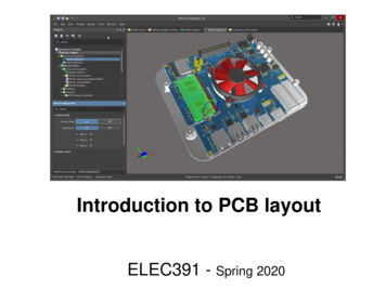
Introduction to PCB layoutELEC391 - Spring 2020
PCB Design support for ELEC391:Altium 2018, 150 licensesTalks: Jan 21 Introduction to PCB layout Mar 16 (TBC) Invited talk: PCB FabricationFabrication deadlines, Mondays:Feb 3, Feb 10, Feb 17, Feb 24, Mar 2, Mar 9, Mar 16Support & submission instructions posted here
Contents PCB design flowHow to install Altium Designer 2018Overview of Altium DesignerDesign example as backdrop to introduce PCBconcepts Instructions for ELEC391 fabrication submissions Reference section: PCB design best practicesCredits: Unless explicitly stated all source material is from the Altium website andAltium training documents. [B1] Complete PCB Design Using OrCad Capture and Layout \ Kraig Mitzner, 20073
PCB Design Flow4
Typical PCB Design flowSeparate toolsor integratedenvironmentsFront-end designand capturehttp://e2e.ti.com/
Typical PCB Design flowFront-end designand capture
Typical PCB Design flowPlacementPhysicalPCBDesignRoutingDRC check
Typical PCB Design flow
Typical PCB Design flowSeparate toolsor integratedenvironmentsFront-end designand capturehttp://e2e.ti.com/
How to installAltium Designer 201810
How to install Altium 2018 Link to instructions:https://www.ece.ubc.ca/ eng-services/Altium/– Create an account at Altium Live:email: engservices@ece.ubc.ca (fast)http://live.altium.com/#signin (slow & not linked to our license)– Download Altium v2018– Connect to license server Access to license server:– Lab PC or a wired connection to ECE network– Wireless connection at UBC (ubcprivate, ubcsecure)– My VPN connection
To set the license server1See instructions online3See instructions online2If you loose connection to server click hereIf you have problems with server, Disconnect from& Reconnect to server
To use a licenseRight click4If you are having problemswith the license server:Disconnect & Reconnect
Getting started with Altium Designer 2018Exploring Altium DesignerAltium Designer documentation:Do complete this tutorialBest training material is on the Altium website. Info is updated, but beware thatmenus and options change between versions. ver 2018 ver 2016
Overview of Altium Designer15
Altium Designer 2018A unified design environmentSystem requirements (MS W7, W8, W10) Front-end design and capture Physical PCB design Mixed-signal circuit simulation Signal integrity analysis Multi-Board Assembly Power Integrity Analyzer PCB manufacturing
Professional Design Environment Unified platform for individual or corporate use Collaborative environment (corporate tool):– Multiple users, some with dedicated tasks– Design team incremental changes day-by-day– Built-in version control (SVN subversion or CVSconcurrent versions system– Design repositories / Vaults (accessible by multipleusers with different credentials Cloud oriented support:– Save preferences online– http://live.altium.com/ (forum, design content, blog)– Altium Vault (dynamic library of components)
Advice for ELEC391 Keep it simple Focus on schematic entry & layout One page schematics Locate the right library models for your parts Stay away from very small SMD components Remember that ECE will take care of CAD filegeneration and fabrication
Altium Design X2 Environment
Recommended basic panelsLibraries&Vault ExplorerProjectsMessagesFor more help working with panels read this
Preferences Dialog
Tips(Basics for the single user) Use Keyboard shortcuts Shift F1 while running a command for alist of shortcuts Esc or Right Click to exit acommand mode Save documents and projectoften
Design Example23
Design exampleL298 Motor Driver Board( by Matt Winship)L298 Motor Driver Board Datasheet.pdf3D View on Layout Editor
Create project files1. Project file2. Schematic file3. PCB fileWhen creating the projectfile remember to use“Save As” to rename.Otherwise your project willbe called “PCB Project1”Create Schematic &PCB files.Remember to renameaccordingly.It is good practice tosave all files in thesame directory
L298 Motor Driver Board PartsDatabaseV16.1.IntLibQ-LN298HSAdditional Parts .1.IntLib
Steps to create the Schematic1. Load libraries2. Draw the schematicSet electrical type for connector pins3. Compile Project:Project Project OptionsMore on: Compiling and Verifying the Design4. Place no ERC labels if necessaryModify connection matrix with cautionMore on: No ERC Directive
Wiring Tips Left-click or Enter to anchor the wire at the cursor position. Backspace ( ) to remove the last anchor point. Spacebar to toggle the direction of the corner. Shift Spacebar to cycle through all possible corner modes.Right-click or Esc to exit wire placement mode.To graphically edit the shape of a wire, Click once to select itfirst, then Click and hold on a segment or vertex to move it. Whenever a wire crosses the connection point of acomponent, or is terminated on another wire, a junction willautomatically be created. A wire that crosses the end of a pin will connect to that pin,even if you delete the junction. To move a placed component and drag connected wires withit, hold down the Ctrl key while moving the component, orselect Move » Drag.
About LibrariesMore on: Understanding Models, Components and Libraries Component representationsfor different phases of design:– Schematic symbol– PCB footprint– SPICE model definitions– Signal integrity description– 3D graphical description
Libraries collection of components Collection of components, models or both Model Libraries (*.MDL, *.CKT, *.PCBLib)– Simulation models are one file per model– PCBLib libraries are typically a collection of footprints Schematic Libraries (*SchLib)– Symbol and a link to a model library Integrated Libraries (*.IntLib)– Symbol, footprint and other models are compiled intoa single portable file to create – Unified components with links to all domain models parametric information
Obtaining integrated libraries1.Altium default librariesMiscellaneous ConnectorsMiscellaneous Devices2.Altium VaultCloud dynamic collection of unified componentsincludes real-time supply chain information3.Frozen (legacy) libraries: from hereyou can install anywhere but it is a good idea to make a subfolder under:C:\Users\Public\Public Documents\Altium\AD18\Libraryor a cloud storage service if you work from more than one PC4.AltiumLive website: Resources / Design Content5.6.7.IC Manufacturer sites (specially simulation models)ELEC391 libraries from last year: hereMake your own
Accessing libraries1. Library Panel2. Explorer Panel(with an Altium Live account)
Configuring librariesProject: part of and available only to theactive project and its documentsYou have to keep track of where these areif you move the project filesInstalled: All installed libraries.Components are available to all openprojects and list is persistent acrossdesign sessionsSearch Path: Additional Librariesaccessible via a search path and subfoldersThe search paths are valid for theactive project
Current librarySelect a different librarySet library browse modeSearch in current libraryList of components.Select the component ofinterestLibraries Panel:All libraries available to theactive projectProject Installed SearchPathWhen placing component:Schematic symbol forselected component spacebar to rotate x or y to flip Tab open properties dialogModels linked to theselected component L for PCB footprintsto flip component sideGraphical display of theselected modelTo search across libraries:Icons used to show/hidepanel sectionsSearch
How to select items from the Vault?Often you will get several choices for the same part, e.g.These are typically different component or shipping packagingoptions. Read the description and check the footprints carefullyBulk (TO-92) loose partsAmmo Box (TO-92)RoHS Compliance2N2222 (TO-18)2N2222 (3-Pin SMD)
Through-hole Packages & Components Use holes drilled through the PCB for mounting thecomponents which are (typ.) soldered on the bottom layer Dual in-line package, DIPn DIP14Pin spacing is 0.1”TTL, CMOS, Linear (Analog) ICs
Surface Mount Packages Use SMD for high density, small parasitics, or a specific IC Passives Flatchip (ceramic Rs, Cs) 4-digit size codehttp://www.topline.tv/SMT Nomenclature.pdf
Surface Mount PackagesDifficult tosolder by hand There are many types of packages (with leads, lead-less) List of integrated circuit packaging types (wikipedia)List of integrated circuit package dimensions Good visual reference is the NXP postersDiscretes package poster.pdfDiscrete Flat No-leads DFN package poster.pdf
Ref [B1]Footprints are made out of pads Pads: contact areas for soldering components, test points, and solder trapsPads can have any shapeSingle layer pads: Top/bottom layer, common for SMT, end launchconnectorsMulti-layer pads: for through hole componentsFootprints are a collection of pads39
LM298 Motor Driver Board Layout Size 1.2” x 2”2 layersMounting holesThick traces for Vand V Power planesfor Vs and GNDTop MetalBottom Metal
2 starting points for PCB design1. From a companion schematic package–––––Prepare project schematicsImport schematic designComponent footprints are added automaticallyConnectivity is indicated with rats nestsNet names are imported from the schematic2. Directly from the PCB editor– You need to select and place manually eachcomponent footprint from a library– No rats nest – connectivity– You must assign nets manually (at least GND)41
Steps to complete the Layout1. Choose work units (metric or imperial)Setupyou can switch at any time2. Set the grid3. Define the board shapeplan for mounting holes and account for connectors4. Set the originLayoutalthough you can move it for convenience as you work5.6.7.8.9.Transfer the design from the schematicPlace components and mounting holesRouteDraw a board outline, add labels (group #)DRC Check
Working units Imperial (inches) Metric (mm) 1/1000th of an inch 1mil 1thou 100mils (0.1”) is acommon dimension 1 mm 1mil ! Common unit in SMparts Remember: 100mils 2.54mm To switch units in Altium Press Q
About the grid The PCB Editor is a grid based environment Objects are placed on a ‘placement or snap grid’ Placement is assisted such as the user doesn’t need toaim with absolute accuracy Unified Cursor-Snap System Properties Panel User defined grids (Cartesian & Polar), that can startat any location and cover different size areasDefault snap grid is called: Global Board Snap Grid Press G to set Global grid step, define grids etc. You can work with just the Global Grid, and adjust thestep to coarse when placing parts, and fine values whenrouting More about the PCB Grid system here44
PCB Editor view modes Viewing modes: Board Planning Mode 1 – Design » Edit Board Shape– Design Move Board Shape 2D Layout Mode 2 3D Layout Mode 3 45
Design transferSetup stepsDesign Update PCB Document Rat’s nests indicate connectivity as perschematic (Net names are assigned topart terminals)All parts in the schematic with their selected footprints
PCBs are multi-layer entitiesTop view all layersTop overlay layerTop copper layer
This is a 2 layer PCB1 dielectric substrate withtop and bottom copperTop overlayTop solder maskTop copperPlated holes and viasBottom copperBottom solder maskYou as a designer specify thelocation of objects andfeatures of every layerHoles, vias, and footprints aregrouped multi-layer objectsMore complex PCBshave a stack-up ofmultiple boards andhence more layers
PCB LaminatesRef [B1] Substrate (laminate)– Rigid board of insulating material, provides structural support.– Available in different materials and thicknesses, e.g:FR4, Rogers/Duroid, Teflon (PTFE)8mils (0.2mm) 240mils(6.1mm)– Most commonly used material type is FR4, 62mils thick– Available with different copper thicknessesCu thickness measured in weight oz/ft2½ oz 0.7mils1 oz 1.4mils2 oz 2.8mils1mil 25μm49
PCB Anatomy: Layer StackupDesign Layer Stack Manager This will enable additional layers as requiredInformation on substrate thickness, type and dielectric is not included in GerberCAM files, these need to be explained separately to the manufacturer.This is a two-sided board with only: Top Layer & Bottom Layer50
Working with Layers Use the tabs at the bottom of the editor to switchbetween layersTo switch to single layer mode To set relevant layersView » Panels » View Configurationor press L Shift S
Configuring the Display Layers Electrical layers32 signal layers and 16 internal power plane layers. Mechanical layers32 general purpose mechanical layers, used for design tasks suchas dimensions, fabrication details, assembly instructions, or specialpurpose tasks such as glue dot layers. These layers can beselectively included in print and Gerber output generation. They canalso be paired, meaning that objects placed on one of the pairedlayers in the library editor, will flip to the other layer in the pair whenthe component is flipped to the bottom side of the board. Special layersthese include the top and bottom silkscreen layers, the solder andpaste mask layers, drill layers, the Keep-Out layer (used to definethe electrical boundaries), the multilayer (used for multilayer padsand vias), the connection layer, DRC error layer, grid layers, holelayers, and other display-type layers.52
Mechanical Layers Multi-purpose layers E.g. Altium supports 32 Mechanical layers: M1 M32 Typically–––––––M1 Board outlineM2 PCB manufacturing infoM11-M12 Top and bottom layer dimensionsM13 Top layer 3D models and mechanical outlinesM14 Bottom layer 3D models and mechanical outlinesM15 Top layer assembly informationM16 Bottom layer assembly information53
Positioning components & routingPlace a plane on top for GNDPlace a plane bottom for Vs54
Positioning components & routing When placing components:– Try to align parts (same orientation)– Ensure that labels are all set in the same direction– Beware of bulky connectors (use 3D view withcaution)Yellow (top overlay) linesin footprints typically markthe physical boundaries of a partHowever you must be cautious andthink about it.This footprint includes the space takenby a heatsink, but does not show it inthe 3D view
Ref [B1]About Traces / Tracks Copper traces are patterned either by:– Photolithography: requires photomasks– Laser: used to draw patterns on photoresist– Mechanical milling: Cu is removed to isolatethe traces. Trace width and thickness determines:– Ampacity (current carrying capacity)– Characteristic impedance for RF designs Practical limitations:– Minimum trace width and gap for e.g.7mils/7mils is typical fab. spec.Negative view:Copper planes, Drillholes, Solder Masks56
Determining trace widthUse the following online trace width 2006/01/31/pcb-trace-width-calculator57
Handy shortcuts for routing Press * on the numeric keypad while routing to cycle through theavailable signal layers. A via will automatically be added, inaccordance with the applicable Routing Via Style design rule.Alternatively, use Ctrl Shift Roll shortcuts to move back and forththrough the available signal layers. Shift R to cycle through the enabled conflict resolution modes,including Push, Walkaround, Hug and Push, and Ignore. Enable therequired modes in the PCB Editor - Interactive Routing page ofthe Preferences dialog. Shift S to cycle single layer mode on and off, ideal when there aremany objects on multiple layers. Spacebar to toggle the corner direction (for all but any angle mode). Shift Spacebar to cycle through the various track corner modes.The styles are: any angle, 45 , 45 with arc, 90 and 90 with arc.There is an option to limit this to 45 and 90 in the PCB Editor Interactive Routing page of the Preferences dialog.58
Design Rules Design RulesRuleElectrical, ClearanceRouting, Width*ConstrainQueryMin clearance 7milAllMin width 7milsMax width 500milsPreferred 10milsAllRouting, Width IOMin width 7milsMax width 500milsPreferred 100milsAdvanced (Query)(InNet(‘V ') ORInNet(‘V-'))Width VssMin width 7milsMax width 500milsPreferred 20milsNet Vss59
Custom Routing design rulesRename to “Width IO’Use ‘Custom Query’ to set”Belongs to net V ORBelongs to V-Set rule executionpriority
Auto route Rout » Un-Route » All Auto Route » All You can also setsingle layerrouting
Ref [B1]HolesHoles can be: Vias, multi-layer pads,mounting holes, or cutsAltium pad properties dialog Plated or non platedYou must specify whether a hole is plated ornon plated during the design processPlating reduces hole size by 0.003”62
Hole sizes Comon hole sizes: non-plated vs. plated sizesDrillNumberSetDrillSizeFinished SizeApproximate Use#76.020".017"via holes#70.028".025"via holes, fine lead devices such as trim pots etc.#65.035".032"IC's, 1/4 watt resistors, small diodes, ripple caps etc.#62.038".035"Square posted pins that measure .025" on the flat.#58.042".039"TO-220 packages, IDC type square posted headers,1/2 watt resistors, 1N9000 series diodes, IC chipcarriers, etc.#55.052".049"larger connectors, transformer leads, etc.#53.060".057"similar to .052" above#44.086".083"TO-220 mounting holes, screw holes, general mounting1/8 in.125".122"mounting holes#24.152".149"mounting holes
Ref [B1] Connection between layers is accomplished with via holesAfter the holes are drilled, their inner walls are platedTop and bottom traces are patterned after platingThermal relief is neededwhen connecting a viato a copper planePWR and GND planesare commonly innerlayersTeardrops:64Source: wikipedia.org: Thermal padVias
Ref [B1]Types of Vias Types of via holes:– Plated and un-platedthrough-hole, blind, buried65
Ref [B1]Solder mask Solder mask or solder resist:––––Thin polymer layer deposited on top and bottom layersProtects outer layers from oxidation and prevents solder bridgesAllows for wave or reflow soldering of componentsHoles are opened with photolithography wherever componentswill be soldered– Default color is green, but any other color is possibleSource: Printed Circuit Board Basics: An Introduction to the PCB Industry, by: Michael Flatt66
Ref [B1]Legend / Silkscreen / Overlay Legend or silkscreen:– Applied on top of thesolder resist– Can be applied to one orboth outer layers– Default color is white butany other color ispossibleTip: add (Top) and (Bottom)67
Instructions for ELEC391fabrication submissions68
Submission Instructions No limits to # of boards (7 deadlines) Cost: 25 10/ sq-in, from project budget Submission dates:Midnight, MondaysFeb 3, Feb 10, Feb 17, Feb 24,Mar 2, Mar 9, Mar 16we will check submissions and accept fixesuntil 5PM the following Tuesday M T W Th Turn around: 5-6 business daysF Sa SM T W Th F Sa S Work within the given guidelines Verify PCB layout and design - prior to design submission Submissions will be rejected if guidelines are not followed69
We will panelize your designs to speed upfabrication and reduce costsPanelized designs from elec391 Spring 2016
Submission Instructions You can send several different boards per submission You can request several copies of each but that increasesyour area & cost Email pcb@ece.ubc.caSubject: [PCB] ELEC391, Group #, submission# Attach: Zipped file with your PCB Project file (*.PrjPcb) andall associated files, also include the latest DRC report.(make sure all files are under the same directory)Body:Total number of boards to fabricate:Name of boards to fabricate and number of copies for each71
Design constrains 1/21) Layers:1) Maximum number of electrical layers 22) Bottom overlay (PCB underside text) will not be manufactured please use "bottom layer" for bottom text2) Try to minimize the size of your PCBComponents can be placed side by side (recommend 50-100 mil IC'sseparation for most cases3) Do not forget to:Add your group number on the top overlay – make it visibleDraw a board outline on layer “Mechanical 1”if several boards in a single file, draw a board outline for each(min spacing from edge of board for any feature is 10mils)72
Design constrains 2/24) Install provided Design-Rules file (available here)please do not modify base rules, but you can add customrouting rules.Submissions that do not pass DRC will be rejected73
How to load design rule file DRC file and these same instructions from here Download and save as “.RUL” file On your PCB design select:Design Rules On the 'PCB Rules and Constrains Editor', Rightclick anywhere on the left column– Select: Import Rules– Select all rules in window (using shift and mouse or Ctrl A ) OK– Browse to select .RUL file– Clear existing rules prior to import? NO74
Component clearance and (electrical) clearance:– Minimum distance 7 mil (Routing) width:– Minimum trace width 7 mil Annular ring size:– Minimum annular ring size 7 mil– Minimum annular ring size for vias 5 mil Board outline clearance: 10mils No limit to allowed hole sizes75
PCB Design Best Practices
Best Practices: Estimating board size Before starting layout it is good tohave an idea of the target size ofthe PCB board and all otherrelevant dimensions.wasteful It is very helpful to have thecomponents at hand to plan thefloor-plan. An old good trick of the trade is toprint the PCB layout at a 1:1 scale,place the printout on a foam andstick on the through e-perfect-pcb-prototype/77
Best Practices: Floor planning Choose your units and set the grid Carefully plan the placement of components–––––––Place analog and digital sections apartGroup components into ‘functional blocks’Place ICs in the same directionAlign ICs, resistors, labels, capacitors etc.Place de-caps close by their ICsPlace Op-amp resistors near the Op-ampPlan for mounting holes and heat sinks Aim for symmetry when possible Do use Design Rule check78Background: Apple Macintosh PCB from http://www.digibarn.com/collections
Best Practices: Routing strategy On two sided boards keep traces perpendicular as much as possible Avoid 90 degree bends in tracks (reduced chances of acid traps) Keep traces a short as possible Always connect a trace to the center of the pad Use teardrops (Tools tear drops), and use vias to avoid lockout Do not place vias under SMD pads Layout first all critical tracese.g. CLK, diff pairs, controlled length Polygons as fills:Connect to GND (EMC), or do not leave ‘dead copper’ Rout nicely[Ref 3]79
Best Practices: Labelling Always sign your design: add date,version, and name of board Label all relevant inputs and outputs Default sizes for comments anddesignators are 60mils x 10mils If you have silkscreen on both sidesadd a 'TOP' label to the top overlay.80
Best Practices: Finishing touches Add mounting holes Confirm Board Information– Properties panel: Board information section (when noobjects are selected)– Click on Reports and select: Board Specifications Non-Plated Hole Size Plated Hole Size Using the hole size editor:– Minimize the total number of holes sizes– Verify that all vias are the same size (if possible) Verify that there are no unwanted leftovers onany Mechanical layer81
Online resources1. Ten best practices of PCB design – EDNMagazine, Edwin Robledo & Mark Toth2. Circuit Board Layout Techniques – TexasInstruments, Chapter 17 of Op-amps foreveryone3. PCB Design Tutorial – David L. Jones82
1. Altium default libraries Miscellaneous Connectors Miscellaneous Devices 2. Altium Vault Cloud dynamic collection of unified components includes real-time supply chain information 3. Frozen (legacy) libraries: from here you can install anywhere but it is a good idea to make a subfolder under: C:\Users\Pub