Transcription
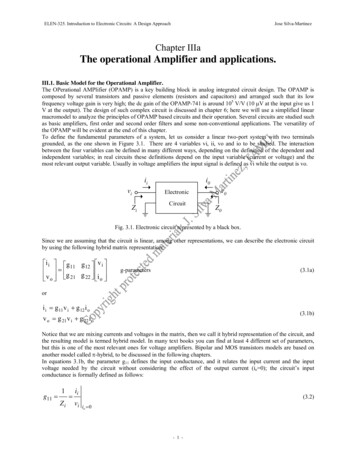
ELEN-325. Introduction to Electronic Circuits: A Design ApproachJose Silva-MartinezChapter IIIaThe operational Amplifier and applications.III.1. Basic Model for the Operational Amplifier.The OPerational AMPlifier (OPAMP) is a key building block in analog integrated circuit design. The OPAMP iscomposed by several transistors and passive elements (resistors and capacitors) and arranged such that its lowfrequency voltage gain is very high; the dc gain of the OPAMP-741 is around 105 V/V (10 V at the input give us 1V at the output). The design of such complex circuit is discussed in chapter 6; here we will use a simplified linearmacromodel to analyze the principles of OPAMP based circuits and their operation. Several circuits are studied suchas basic amplifiers, first order and second order filters and some non-conventional applications. The versatility ofthe OPAMP will be evident at the end of this chapter.To define the fundamental parameters of a system, let us consider a linear two-port system with two terminalsgrounded, as the one shown in Figure 3.1. There are 4 variables vi, ii, vo and io to be studied. The interactionbetween the four variables can be defined in many different ways, depending on the definition of the dependent andindependent variables; in real circuits these definitions depend on the input variable (current or voltage) and themost relevant output variable. Usually in voltage amplifiers the input signal is defined as vi while the output is vo.iiviZii0ElectronicCircuitv0Z0Fig. 3.1. Electronic circuit represented by a black box.Since we are assuming that the circuit is linear, among other representations, we can describe the electronic circuitby using the following hybrid matrix representation: i i g11 g12 v i v o g 21 g 22 i o g-parameters(3.1a)ori i g11 v i g12 i o(3.1b)v o g 21 v i g 22 i oNotice that we are mixing currents and voltages in the matrix, then we call it hybrid representation of the circuit, andthe resulting model is termed hybrid model. In many text books you can find at least 4 different set of parameters,but this is one of the most relevant ones for voltage amplifiers. Bipolar and MOS transistors models are based onanother model called -hybrid, to be discussed in the following chapters.In equations 3.1b, the parameter g11 defines the input conductance, and it relates the input current and the inputvoltage needed by the circuit without considering the effect of the output current (io 0); the circuit’s inputconductance is formally defined as follows:g11 1Zi iivi(3.2)io 0- 1 -
ELEN-325. Introduction to Electronic Circuits: A Design ApproachJose Silva-MartinezThis parameter is measured by applying an input voltage source and measuring the input current; the output node isleft open such that io 0. Since g11 is the ratio of the input current to the input voltage, while the output is leavedopen, its units are amps/volts or 1/Ω.The parameter g12 defines the reverse current gain of the topology, and it is defined asg12 iiio(3.3)vi 0This parameter represents the reverse current gain: current generated at the input due to the output current. In theideal case this parameter is zero since usually the operational amplifiers are unidirectional; e.g. the input signalapplied to the system generates an output signal, but the output signals (current or voltage) should not generate anysignal at the input. For measuring this parameter it is required to short circuit the input port such that vi 0, thenapply a current at the output and measure the current generated at the input port. In practical circuits this parameteris very small and usually it is ignored.The Forward voltage gain is defined as the ratio of the output voltage and input voltage without any load connectedat the output.g 21 AV vovi(3.4)io 0This is certainly one of the most important parameters of the two-port system; we also refer to AV as the open-loopgain of the OPAMP. It represents the circuit’s voltage gain without any load impedance attached (output currentequal zero).Another important parameter is the system’s output impedance, which relates the output voltage and the outputcurrent without taking the effects of the input signal. It is defined byg 22 Z 0 voio(3.5)vi 0Thus, the two-port system can be represented by the four aforementioned parameters; the resulting macromodel isshown in Figure 3.2. For sake of clarification we are using impedances instead of admittances in this representation.Notice that a current controlled current source (ICCS) is used for the emulation of parameter g12 since it representsthe input current (input port) being generated by the output current (output port). A resistor can not represent thisparameter since current is flowing in one port but the voltage at the other port controls it. Similar comments apply tothe voltage controlled voltage source represented by AV vi (g21vi).i0iiviZ0Zig12i0 -v0AVviFig. 3.2. Linear macromodel of a typical voltage amplifier using hybrid parameters.Model for the OPAMP. The ideal OPAMP is a device that can be modeled by using the circuit of Fig. 3.2 withAV , g12 0, Zi , and Zo 0. This is of course an unrealistic model, but it is enough for understanding the basiccircuits and their operation. We will see that when you connect several circuits in cascade for complex signal- 2 -
ELEN-325. Introduction to Electronic Circuits: A Design ApproachJose Silva-Martinezprocessing, both input and output impedances are important parameters that affect the overall performance of thesystem. In this section, however these effects are not considered.Discuss here the main limitations such as input impedance, limited DC gain and DC offsets and input bias current.III.2. Basic configurations: Inverting and non-inverting amplifier.Inverting configuration. The first topology to be studied is the inverting amplifier shown in fig. 3.3a. It consists ofan impedance connected between the input source and the OPAMP’s inverting terminal; the second impedance isconnected from the inverting terminal to the output of the OPAMP. Z2 provides a negative feedback (connecting theOPAMP’s output and the negative input); this is the main reason for the excellent properties of this configuration.The simplified linear macromodel of the OPAMP is used for the representation of the inverting amplifier, and theequivalent circuit shown in fig. 3.3b. By using basic circuit analysis techniques it can be easily find thatvi v xZ1 vo v xZ2 0(3.5)andv o A v v x(3.6)Solving these equations as function of the input and output voltages yields; vo1 vi 1 1 Z 2 Z1 AV Z 2 Z1 (3.7)This relationship is also known as closed-loop amplifier’s gain since the feedback resistor in combination with theOPAMP form a closed loop. If the open-loop gain of the OPAMP AV is very large, then the first factor can beapproximated as unity and the closed-loop voltage gain becomesvovi Z2(3.8)Z1This result shows that if negative feedback is used and if the open-loop gain of the OPAMP is large enough, theoverall amplifier’s voltage gain depends on the ratio of the two impedances. Unlike to the gain of the open-loopgain of the OPAMP that can vary by more than 50 % due to transistor’s parameters variations and temperaturegradients, as will be explained in the following sections, the closed loop gain is quite accurate, especially if sametype of impedances are used. Usually ratio of impedances is more precise than the absolute value of components;e.g. ratio of capacitors fabricated in CMOS technologies can be as precise as 99.5 % while the absolute value of thecapacitance may change by more than 20%.Z1 viZ2iiZ2vi Z1vov0 -A vV x-vx-(a)(b)- 3 -
ELEN-325. Introduction to Electronic Circuits: A Design ApproachJose Silva-MartinezFig. 3.3. Inverting amplifier: a) the circuit and b) the linear macromodel assuming that OPAMP input is infinity andoutput impedance is zero.Another important observation is that the differential voltage at the OPAMP input vx (see Fig. 3b) is ideally zero.The reasoning behind this observation is as follows: according to 3.8, the output voltage is bounded (not infinity) ifZ1 is not zero or Z2 is not infinite, hence vi is also bounded. Under these conditions and according to expression 3.6the OPAMP input voltage vx is very small if Av is large enough; the larger the OPAMP open loop gain the smallersignal at the input of the OPAMP. Therefore the inputs of the OPAMP can be considered as a virtual short; thevoltage difference between the two input terminals (v - v-) is very small but they are not physically connected.The virtual short principle is extremely useful in practice; most of the transfer functions can be easily obtained if thisproperty is used. To illustrate its use, let us consider again the circuit of fig. 3.3b. Due to the virtual ground at theinput of the OPAMP, vx 0 (virtual short) and the input current ii is determined by vi/Z1. Since the input impedanceof the OPAMP is infinite, ii flows throughout Z2, leading to an output voltage given by –iiZ2. As a result, theclosed-loop voltage gain becomes equal to -Z2/ Z1, as stated in equation 3.8.If the impedances Z1 and Z2 are replaced by resistors as shown in Fig. 3.4a, we end up with the basic resistiveinverting amplifier. The closed-loop gain is then obtained asR2R2R1viR1vo- - vivo(a)(b)Fig. 3.4. Resistive amplifiers: a) inverting configuration and b) non-inverting configuration.vovi R2(3.9)R1Notice that in the case of the inverting configuration, the amplifier’s input impedance is determined by R1; this is aresult of the virtual ground present at the inverting terminal of the OPAMP. Hence, if several inverting amplifiersare connected in cascade we have to be aware that the amplifier must be able to drive the input impedance of thenext stage.Non-inverting voltage gain configuration. If the input signal is applied at the non-inverting terminal and R1 isgrounded, as shown in fig. 3.4b, the non-inverting configuration is obtained. Notice that the feedback is stillnegative. If R2 is connected to the positive terminal, the circuit becomes unstable and useless for linearapplications; this will be evident in the following sections. The closed-loop voltage gain of the non-invertingconfiguration can be easily obtained if the virtual short principle is used. Due to the high gain of the OPAMP, thevoltage difference between the inverting and non-inverting terminals is very small; hence the voltage at the noninverting terminal of the OPAMP is also vi. The current flowing through R1 and R2 is then given by vi/R1; thereforethe output voltage is computed asv o v i i1 R 2 v i v i R 1 R 2R 1 2viviviR1(3.10)The voltage gain is therefore greater or equal than 1. An important characteristic of this configuration is that ideallyits input impedance is infinity; hence several stages can be easily connected in cascade. A special case of the noninverting configuration is the buffer configuration shown in figure 3.5. If R1 , according to equation 3.10, thevoltage gain is unity; in this case the value of R2 is not critical and can even be short-circuited (R2 0). This topologyis also known as unity gain amplifier or buffer, and it is very popular for driving small impedances; e.g. speakers,motors, etc.- 4 -
ELEN-325. Introduction to Electronic Circuits: A Design ApproachJose Silva-MartinezRf-vivo Fig. 3.5 OPAMP in unity gain buffer configurationEmphasis on loading effects; discuss these issues in class!III.3. Amplifier with multiple inputs and superposition.Input signals can be applied to the two inputs of the OPAMP, as shown in Fig. 3.6. R1 and R2 are a voltage divider;the input voltage at the non-inverting (v ) terminal is thenR4R1v vi2R3-vi1voR2Fig. 3.6. Amplifier configuration with two input signals applied to the non-inverting and inverting terminals.v v i2 R2(3.11)R1 R 2If a virtual short at the OPAMP inputs is assumed, the voltage at the inverting and non-inverting terminals is thesame, and determined by v . Using KCL at the inverting terminal of the circuit leads tovo v R4 v v i1(3.12)R3Using equations 3.11 and 3.12, the output voltage is obtained, yielding R4 R2 R4 v 1 vo vi1 R R R i 2 R 2 3 1 3 (3.13)Notice that the output voltage is a linear combination of the two input signals: the first component is determined bythe vi1 and the other one determined by vi2. This analysis can always be used, but we can also take advantage of theproperties of linear systems.Superposition principle for a linear system. If the OPAMP is considered as a linear device and onlylinear impedances are used, then the output voltage is a linear combination of all the inputs applied. If severalinputs are applied to the linear circuit, then the output can be obtained considering each input signal at a time; e.g.grounding all other input signals and applying the input signal under study. Therefore, the following property holds:if- 5 -
ELEN-325. Introduction to Electronic Circuits: A Design ApproachN v o v i1, v i 2 ,., v iN k j v ijj 1 Jose Silva-Martinez (3.14a)vik k j 0 thenv o v i1, v i 2 ,., v iN v o v i1 ,0.0 v o 0, v i 2 ,.0 v o 0,0,.v iN (3.14b)This property is known as the superposition principle. Let us apply this principle to the topology shown in Fig. 3.6,where two inputs are applied to the amplifier. The circuit is analyzed by applying one input signal at a time: if vi1 isconsidered, vi2 is made equal zero. The equivalent circuit is shown in Fig. 3.7a.R4R4R3vovi2R1 v R1 R2vo -v -R3vi1R2(a)(b)Fig. 3.7 Equivalent circuits for the computation of the output voltage: a) for vi1 and b) for vi2.Since the input impedance of the OPAMP is infinite, the current flowing through R1 R2 is zero, and v 0. Theresulting circuit is the typical inverting amplifier where the output voltage is given by -(R4/R3)vi1; notice that thisoutput corresponds to the first term in equation 3.13. If the first input is grounded and signal vi2 is considered, theresulting equivalent circuit is depicted in fig. 3.7b. The voltage at the non-inverting terminal is given by equation3.11, and the output voltage is equal to vo (1 R4/R3)v ; the final result leads to the second term of equation 3.13.Generalization of basic configurations. The concepts of infinite input impedance, zero output impedance, virtualshort of the OPAMP inputs and linear superposition are especially useful when complex circuits are designed. Ananalog inverting adder is shown in fig. 3.8a; the output voltage can be easily found if we apply the superpositionprinciple to each input. The equivalent circuit for the jth-input is depicted in fig. 3.8b. Since only Rj is connected tovij, the resistors connected to the other inputs must be grounded. These resistors are connected between the physicalground and the virtual ground generated by the negative feedback and the large open-loop voltage gain of theOPAMP, as a result of this the current flowing through all grounded resistors is zero, then ij, generated by vij, Rj andthe virtual ground node vx ( 0) flows throughout Rf. The output voltage is then obtained as –(Rf/Rj)vij. By using thesame concept to all inputs, the amplifier’s output voltage is found asR1RfiNviN RJ-vijRfijvijvoRNRJvx 0 ij-vi1i1 R1voRNFig. 3.8. a) Analog adder and b) equivalent circuit for analyzing the output voltage due to vij.- 6 -
ELEN-325. Introduction to Electronic Circuits: A Design ApproachN Rfvo j 1 R jJose Silva-Martinez v ij (3.15)An interesting advantage of this circuit is that each one of the input resistors independently controls the voltage gainfor each input. This is an important circuit property used for the design of analog-digital converters for instancewhere the addition of binary weighted signals are required.An analog non-inverting adder is depicted in fig. 3.9a. Similarly to the previous case, the output voltage can becomputed by using superposition. Shown in fig. 3.9b is the equivalent circuit for the jth-input signal, and making allother inputs equal zero. The voltage at the non-inverting terminal is the result of the voltage divider determined bythe resistors lumped to node v j as follows:RfRJ viNR1voR1vijRXRNRJvo vij-vi1Ri-RiRfv jRXRNa)b)Fig. 3.9. a) Non-inverting amplifier with multiple inputs and b) equivalent circuit for the jth input.v jv ij RR 1 R 2 R J 1 R J 1 R N R X1 (3.16)R 2 R J 1 R J 1 R N R X R JSince many components are in parallel, for the analysis of this type of networks it is very often more convenient touse admittances instead of impedances. For this example, the previous equation can also be expressed as1v jRJ(3.16b) 11v ij R J R 1 R 2 R J 1 R J 1 R N R XThe numerator (1/Rj) is identified as the admittance of the element connected between the input signal and v j. Thedenominator represents the parallel of all elements attached to v . The parallel connection of impedances is alsoequivalent to the reciprocal of the addition of their admittances; then 3.16 can be expressed by the followingequivalent expressionv jv ij gJ(3.17)N g i g Xi 1where gi 1/Ri. Once v j is obtained, the output voltage generated by vij can be obtained. Since v j is the voltage atthe non-inverting terminal, to find the output voltage for this input is straightforward as voj (1 Rf/Ri)v j. Taking intoaccount all the input signals and applying the superposition principle, it can be shown that the overall output voltageis a linear combination of all inputs; the result of this analysis yields,- 7 -
ELEN-325. Introduction to Electronic Circuits: A Design Approach R f R f N g J v ij v o 1 v j 1 R i J 1R i j 1 N g i g X i 1NJose Silva-MartinezRf 1 Ri N g i g X i 1 N g J v ij j 1 (3.18)Each input signal has a contribution to the output voltage that depends of all resistors, unlike the case of theinverting topology. The input impedance for each input depends on the array of resistors; for instance the inputimpedance seen by the jth-input signal isZ j R J R 1 R 2 R J 1 R J 1 R N R X (3.19)Similar expressions can be obtained for all other input sources.Example: Design a circuit that implements the following equation:vo t 10 v1 20 v 2 5If needed use the supply voltages /- 15 V. The circuit shown below can be used; this is not the only solution,combinations of inverting and non-inverting circuits might be used as well. The design process consists of findingthe resistance values. For that purpose, the following equations must be solved:R5R4 v2-v1R1voR2R3 15 R10 1 5 R4 g1 g g g23 1 R20 1 5 R4 g2 g g g23 1 R5 1 5 R4 g3 g 1 g 2 g 3 Solve this set of equations, and find the numerical values; it is evident that g1 2g3 and that g2 4g3.III.4. Amplifiers with very large gain/attenuation factors.Very large gain amplifiers require large spread of the components. In analog integrated circuits design, it is difficultto control properly such large ratios, and very often they are very demanding of silicon area. Some configurationsallow us to reduce this spread.Large gain inverting amplifier using resistors in a T-array. Large voltage gain factors require very large resistors;the array of resistors shown in figure 3.10can be used to “increase” the effective feedback resistor. The circuit’stransfer function can obviously be obtained by using conventional circuit analysis techniques such as KCL. It ishowever to useful to analyze the circuit based on the following observations:- 8 -
ELEN-325. Introduction to Electronic Circuits: A Design Approach1.Jose Silva-MartinezSince the inverting terminal is at the ground potential due to the virtual short at the OPAMP input, theresistor R2 is connected between node vx and (virtual) ground; then it is in parallel with R3 if you analyzethe circuit from the output. Therefore, the voltage vx can be computed as R2 R3 vvx R R R 04 2 3(3.20)Notice that vx is an attenuated version of the output voltage.2.Also, as a result of the virtual ground at the OPAMP’s input, the current flowing through R2 is given byvx/R2. If the OPAMP is ideal, the current flowing through R1 is equal to the one flowing through R2, andthen the output voltage can be computed from the following expression:viR1 R2 R3 v0 R2 R2 R3 R4 R2vx (3.21)Therefore, the voltage gain is R2 R3 R4 R2 vi R2 R3 R1 v0(3.22)The voltage gain is therefore equivalent to the gain of a two-stage amplifier; larger gain factors are obtained withreduced resistive spread.R2vx R4R3ii-R1 vivoFig. 3.10. Resistive voltage amplifier for high-gain applications.If further reduction on the resistive spread is needed, two T-networks can be used as shown in Fig. 3.11. Similarly tothe previous case, the voltage vx is equal to –(R2/R1)vi; notice that vx is an attenuated version of vy and this lastvoltage is an attenuated version of vo. These voltages are related by the following expressions: R 2 R 3 vx v y R 2 R 3 R 4(3.23)- 9 -
ELEN-325. Introduction to Electronic Circuits: A Design Approachvyv0 Jose Silva-Martinez R 2 R 3 R 4 R 5 R 2 R 3 R 4 R 5 R 6(3.24)Then the closed loop voltage gain is obtained as vvo o vyvi v y v x v x v in R 2 R 3 R 4 R 5 R 6 R 2 R 3 R 4 R 5 R 2 R 3 R 4 R 2 R 2 R 3 R 1 (3.25)This voltage gain can be very large; it is in fact determined by multiplication of 3 terms, which is equivalent to a 3stage amplifier. Notice that the input impedance of the non-inverting circuit is determined by R1.R2vx R4 vy R6R3R1-viR5vo Fig. 3.11. Resistive amplifier using a T-configuration for large gain factorsVery large attenuation factors. The T-network can also be used for the design of large attenuation factors, forinstance in applications related to power amplifiers where the input signal might be in the range of 100 V or morebut the OPAMP can handle only 12 V or less. The resulting circuit using a T-network at the input is shown in figure3.12. The voltage vx is an attenuated version of the incoming signal, and the voltage gain is adjusted to the properlevel by the typical inverting configuration (R3 and R4). The attenuating factor, considering again a virtual ground atthe input, is determined by R1 and the parallel of R2 and R3; the voltage gain between vx and vo is determined bythe ratio of resistors R4 and R3. Therefore, the output voltage is given by:R4R1vx R3-viR2vo Fig. 3.12. Resistive amplifier using a T-configuration for large attenuation factorsv0 v0 v i v x v x v i R4 R3 R2 R3 R R R 23 1(3.26)The first factor is the result of the voltage divider at the input of the structure, while the second factor is the result ofthe non-inverting amplification of vx. You can also use the double T-cell structure; it is left to the student to find outthe voltage gain in that case; DO IT, this can be a midterm question.III.5. RC Circuits: Integrators and differentiators.Basic integrators. If the feedback resistor is replaced by a capacitor, we obtain a lossless integrator; the circuit isshown below. In this circuit, the input voltage vi is converted into a current by R1 and the virtual ground present atthe input of the OPAMP, similarly to the case of the resistive amplifier. The resulting current is injected into thefeedback capacitor C2 where it is integrated; the resulting output voltage is the integral of the injected current. The- 10 -
ELEN-325. Introduction to Electronic Circuits: A Design ApproachJose Silva-Martinezanalysis of this circuit can easily be done in the frequency domain where the characteristic impedance of thecapacitor is given by 1/(j C2). The transfer function of the inverting configuration is, as in the previous cases,determined by the ratio of the impedance in feedback and the input impedance, leading to the following result:C2R1-vivo Fig. 3.13. Lossless inverting IntegratorH( s ) vo1 visR 2 C1(3.27)where s j . This circuit has a pole at the origin and a “phantom” zero at (why?). The magnitude response isextremely large at low frequencies, and decreases at higher frequency with a rolloff of –20 dB/decade. The phaseresponse is 90 (-270) degrees and independent of the frequency. Notice that at 1/R2C1, the magnitude of thevoltage gain is unity. Usually this circuit is not used as a standalone device, but is the key building block for highorder filters and analog-digital converters.The combination of resistors and capacitors lead to the generation of poes and zeros; for example, the circuitimplementation of a first order filter is shown in figure 3.14. This circuit is also known as a lossy integrator becausewhile R1 injects charge into C2, the resistor R3 leaks (introduces losses) the charge stored in the capacitor. The gainof this circuit is also determined by the ratio of the equivalent impedance in feedback and the input impedance. Inthis circuit, the equivalent feedback impedance is composed by the parallel of the impedance of the capacitor(1/j C2) and R3. The low frequency gain, where the impedance of the capacitor can be ignored, is determined by theratio of the two resistors; it is evident that the voltage gain is given by –R3/R1. At very high frequencies, theimpedance of C2 dominates the feedback and the circuit behaves as the lossless integrator shown in figure 3.19 (gaindefined by –1/sR1C2). The overall voltage gain is given by:R3C2R1-vivo Fig. 3.14. First order lowpass filterR3H( s ) R1(3.28)1 sR3C 2The low-frequency gain is, as expected, determined by the ratio of the resistors. The pole is located at 1/R3C2,and for frequencies beyond this frequency the voltage gain decresases with a rolloff of –20 dB/decade.The main differences between this circuit and the passive lowpass filter (voltage divider) are twofold: a) in theactive realization (with OPAMP) the low frequency gain can be greater than 1 by adjusting the ratio of the resistorswhile in the passive filter the gain is always less than 1; b) the OPAMP allows us to connect the circuit to the next- 11 -
ELEN-325. Introduction to Electronic Circuits: A Design ApproachJose Silva-Martinezstage without affecting the transfer function; this is due to the small output impedance of the OPAMP. A typicaltransfer function obtained with this circuit is depicted in the following plot;R3/R1 1 R3 10log10 R 1 0 dB P log 1 1 u R C 3 2 R3C22 R3 1 R 1 Fig. 3.15. Magnitude response for a first order filter.The unity gain frequency is another important parameter; it can be obtained by taking the magnitude (or squaremagnitude) of equation 3.28, and equating it to 1. The resulting equation can be solved for the frequency, leading tothe following result (find it yourself) 1 u R C 2 1 2 R2 1 R 1 (3.29)For R2 R1, this frequency is approximately given by u 1/R1C1. Notice that for R2 R1 the solution is imaginary,meaning that the unity gain frequency does not exist; in fact you can not find any frequency where the gain is unityfor an attenuator (dc gain less trhan 1). For R2 R1, the low frequency gain is less than 1; hence the transfer functiondoes not have any intersection with the 0 dB curve.The general first order transfer function can be implemented by using the topology shown in fig. 3.16. Since theelements are in parallel, it is very convenient o find the voltage gain as the ratio of the equivalent input addmittanceand the equivalent feedback addmitance as follows:R3R1C2vi C0voFig. 3.16. General first order filterH s R3 1 sR1C 0 g 3 sC 2 R1 1 sR3C 2 g1 sC 0(3.30)With this circuit, you can design the following filters:(a) Lowpass filters if C0 is removed. The pole’s frequency is given by 1/R3C2(b) Amplifier if C0 and C2 are removed. Gain -R3/R1(c) Amplifier if the resistors are removed. Gain - C0/C2 (not very practical, especially for low frequencyapplications)- 12 -
ELEN-325. Introduction to Electronic Circuits: A Design ApproachJose Silva-Martinez(d) High-pass if R1 is removed. Pole’s frequency at 1/R3C2, and high frequency gain -C0/C2.The high-pass transfer function can also be realized if a series of a capacitor and resistor is used, as shown in thefigure below. Low frequency components are blocked by the capacitor due to its high impedance at low frequencies.At high frequencies the capacitor behaves as a short circuit, and the gain is given by the ratio of the resistors. Usingtypical circuit analysis techniques, the overall transfer function can be obtained asR3C1R2-vivo Fig. 3.17. First order High-pass filter using a series capacitor.H s R3 R1 2R2 sC1R3 sR3C1 1 sR C 2 1 (3.31)A DC zero and a pole located at 1/R2C1 can be observed. After the pole’s frequency the voltage gain is mainlydetermined by the ratio of the resistors –R3/R2.Non-inverting integrator. A non-inverting amplifier is implemented by using the following circuit. It is usually anexpensive implementation, since the topology requires matched elements. The transfer function can be easilyobtained by noting that the voltage at the non-inverting terminal is the result of a voltage divider between R and C(v /vin 1/(1 sRC)). The voltage at the non-inverting terminal is then amplified by a factor 1 plus the ratio of thefeedback impedance 1/sC’ and the resistor R’. The resulting transfer function yields;C'R'-Rv vinvoCFig. 3.18. Non-inverting lossless integrator 1 1 sR 'C' H(s) sR'C'1sRC (3.32)That corresponds to a non-inveting integrator if R’C’ RC; in this case, the voltage gain decreases when thefrequency increases with a r
Fig. 3.2. Linear macromodel of a typical voltage amplifier using hybrid parameters. Model for the OPAMP. The ideal OPAMP is a device that can be modeled by using the circuit of Fig. 3.2 with AV , g12 0, Zi , and Zo 0. This is of course an unrealistic model, but it is enough for understanding