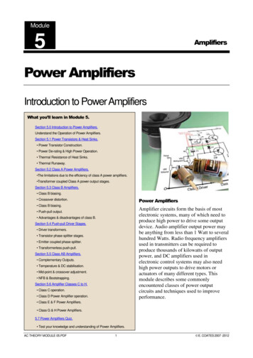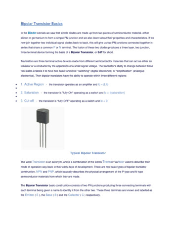
Transcription
6BJT A mplifiersCHAPTER IT THE WEBSITEAmplifier OperationTransistor AC ModelsThe Common-Emitter AmplifierThe Common-Collector AmplifierThe Common-Base AmplifierMultistage AmplifiersThe Differential AmplifierTroubleshootingDevice ApplicationCHAPTER OBJECTIVES Describe amplifier operationDiscuss transistor modelsDescribe and analyze the operation of common-emitteramplifiersDescribe and analyze the operation of common-collectoramplifiersDescribe and analyze the operation of common-baseamplifiersDescribe and analyze the operation of multistageamplifiersDiscuss the differential amplifier and its operationTroubleshoot amplifier circuitsStudy aids, Multisim, and LT Spice files for this chapter areavailable at ntroductionThe things you learned about biasing a transistor in Chapter 5are now applied in this chapter where bipolar junction transistor (BJT) circuits are used as small-signal amplifiers. Theterm small-signal refers to the use of signals that take upa relatively small percentage of an amplifier’s operationalrange. Additionally, you will learn how to reduce an amplifier to an equivalent dc and ac circuit for easier analysis, andyou will learn about multistage amplifiers. The differentialamplifier is also covered.Device Application PreviewThe Device Application in this chapter involves a preamplifier circuit for a public address system. The complete systemincludes the preamplifier, a power amplifier, and a dc powersupply. You will focus on the preamplifier in this chapterand then on the power amplifier in Chapter 7.KEY TERMS r parameterCommon-emitterac groundInput resistanceOutput resistanceAttenuationBypass capacitorCommon-collectorM06 FLOY0103 10 SE C06.indd 255 Emitter-followerCommon-baseDecibelDifferential amplifierCommon modeCMRR (Common-moderejection ratio)23/11/16 6:06 PM
256 BJT Amplifiers6–1A m p l i f i e r O p e rati o nThe biasing of a transistor is purely a dc operation. The purpose of biasing is to establish a Q-point about which variations in current and voltage can occur in responseto an ac input signal. In applications where small signal voltages must be amplified—such as from an antenna or a microphone—variations about the Q-point are relativelysmall. Amplifiers designed to handle these small ac signals are often referred to assmall-signal amplifiers.After completing this section, you should be able to Describe amplifier operationIdentify ac quantities Distinguish ac quantities from dc quantitiesDiscuss the operation of a linear amplifier Define phase inversion Graphically illustrate amplifier operation Analyze ac load line operationAC QuantitiesIn the previous chapters, dc quantities were identified by nonitalic uppercase (capital)subscripts such as IC, IE, VC, and VCE. Lowercase italic subscripts are used to indicate acquantities of rms, peak, and peak-to-peak currents and voltages: for example, Ic, Ie, Ib,Vc, and Vce (rms values are assumed unless otherwise stated). Instantaneous quantities arerepresented by both lowercase letters and subscripts such as ic, ie, ib, and vce. Figure 6–1illustrates these quantities for a specific voltage waveform. FIG U R E 6– 1Vce can represent rms, average, peak,or peak-to-peak, but rms will beassumed unless stated otherwise. vcecan be any instantaneous value onthe curve.VpeakrmsavgVce VceVCEVceVcevce0t0In addition to currents and voltages, resistances often have different values when a circuit is analyzed from an ac viewpoint as opposed to a dc viewpoint. Lowercase subscriptsare used to identify ac resistance values. For example, Rc is the ac collector resistance, andRC is the dc collector resistance. You will see the need for this distinction later. Resistancevalues internal to the transistor use a lowercase r9 to show it is an ac resistance. An example is the internal ac emitter resistance, r9e.M06 FLOY0103 10 SE C06.indd 25623/11/16 6:06 PM
Amplifier Operation 257The Linear AmplifierA linear amplifier provides amplification of a signal without any distortion so that the outputsignal is an exact amplified replica of the input signal. A voltage-divider biased transistorwith a sinusoidal ac source capacitively coupled to the base through C1 and a load capacitively coupled to the collector through C2 is shown in Figure 6–2. The coupling capacitorsblock dc and thus prevent the internal source resistance, Rs, and the load resistance, RL, fromchanging the dc bias voltages at the base and collector. The capacitors ideally appear asshorts to the signal voltage. The sinusoidal source voltage causes the base voltage to varysinusoidally above and below its dc bias level, VBQ. The resulting variation in base currentproduces a larger variation in collector current because of the current gain of the transistor. VCC VbICQVBQR1RCVceRsIbC1F I G U R E 6 –2An amplifier with voltage-dividerbias driven by an ac voltage sourcewith an internal resistance, Rs.IcC2VCEQIBQVsRER2RLAs the sinusoidal collector current increases, the collector voltage decreases. The collector current varies above and below its Q-point value, ICQ, in phase with the base current.The sinusoidal collector-to-emitter voltage varies above and below its Q-point value, VCEQ,1808 out of phase with the base voltage, as illustrated in Figure 6–2. A transistor alwaysproduces a phase inversion between the base voltage and the collector voltage.A Graphical Picture The operation just described can be illustrated graphically on theac load line, as shown in Figure 6–3. The ac signal varies along the ac load line, which isdifferent from the dc load line because the capacitors are seen ideally as a short to the acsignal but an open to the dc bias. The sinusoidal voltage at the base produces a base currentthat varies above and below the Q-point on the ac load line, as shown by the arrows.Determination of the Q-point was discussed in Chapter 5, Section 5–1. The ac load lineintersects the vertical axis (IC) at the ac value of the collector saturation current Ic(sat) andIC IBQGraphical ac load line operation ofthe amplifier showing the variationof the base current, collector current, and collector-to-emitter voltageabout their dc Q-point values. Ib andIc are on different scales.IbIc(sat)IcICQF I G U R E 6 –3Qac load lineVce(cutoff)0VceVCEVCEQM06 FLOY0103 10 SE C06.indd 25723/11/16 6:06 PM
258 BJT Amplifiersintersects the horizontal axis (VCE) at the ac value of the collector-to-emitter cutoff voltageVce(cutoff). These values are determined as follows:Ic(sat) VCEQ Rc ICQVce(cutoff) VCEQ ICQRcWhere Rc is the parallel combination of RC and RL.Lines projected from the peaks of the base current, across to the IC axis, and down tothe VCE axis, indicate the peak-to-peak variations of the collector current and collectorto-emitter voltage, as shown. The ac load line differs from the dc load line because thecapacitors C1 and C2 effectively change the resistance seen by the ac signal. In the circuitin Figure 6–2, notice that the ac collector resistance is RL in parallel with RC, which is lessthan the dc collector resistance RC alone. This difference between the dc and the ac loadlines is covered further in Chapter 7 in relation to power amplifiers.EXAMPLE 6–1Given the Q-point value of ICQ 4 mA, VCEQ 2 V, RC 1 kV, and RL 10 kV fora certain amplifier, determine the ac load line values of Ic(sat) and Vce(cutoff).SolutionThe ac load line values of Ic(sat) and Vce(cutoff) areRc RC 7 RL 1 kV 7 10 kV 909 VIc(sat) VCEQ Rc ICQ 2 V 909V 4 mA 6.2 mAVce(cutoff) VCEQ ICQ Rc 2 V 4 mA (909 V) 5.64 VRelated Problem*If the Q-point is changed to 3 V and 6 mA, what is the intersection values of the acload line on the two axes?* Answers can be found at www.pearsonhighered.com/floyd.EXAMPLE 6–2AF IGU R E 6 – 4mIb50A60 The ac load line operation of a certain amplifier extends 10 mA above and below theQ-point base current value of 50 mA, as shown in Figure 6–4. Determine the resultingpeak-to-peak values of collector current and collector-to-emitter voltage from the graph.m40AIC (mA)87Icm70 mA660 mAQ550 mA440 mA330 mA220 mA110 mA10234VCE (V)VceM06 FLOY0103 10 SE C06.indd 25823/11/16 6:06 PM
Transistor AC Models 259SolutionRelated ProblemSECTION 6–1CHECKUPAnswers can be found at www.pearsonhighered.com/floyd.6–2Projections on the graph of Figure 6–4 show the collector current varying from 6 mAto 4 mA for a peak-to-peak value of 2 mA and the collector-to-emitter voltage varyingfrom 1 V to 2 V for a peak-to-peak value of 1 V.What are the Q-point values of IC and VCE in Figure 6–4?1.2.3.4.When Ib is at its positive peak, Ic is at its peak, and Vce is at its peak.What is the difference between VCE and Vce?What is the difference between Re and re9?Why is the ac resistance seen by the collector different from the dc resistance?T r an s i s tor AC M o d e l sTo visualize the operation of a transistor in an amplifier circuit, it is often useful torepresent the device by a model circuit. A transistor model circuit uses various internaltransistor parameters to represent its operation. Transistor models are described in thissection based on resistance or r parameters. Another system of parameters, calledhybrid or h parameters, is briefly described.After completing this section, you should be able to Discuss transistor modelsList and define the r parametersDescribe the r-parameter transistor modelDetermine r9e using a formulaCompare ac beta and dc betaList and define the h parametersr ParametersThe r parameters that are commonly used for BJTs are given in Table 6–1. Strictly speaking,aac and bac are current ratios, not r parameters, but they are used with the resistance parameters to model basic transistor circuits. The italic lowercase letter r with a prime denotesresistances internal to the transistor.r PARAMETERSDESCRIPTIONr9eac emitter resistancer9bac base resistancer9cac collector resistanceaacac alpha (Ic Ie)bac TA B L E 6–1r parameters.ac beta (Ic Ib)r-Parameter Transistor ModelAn r-parameter model for a BJT is shown in Figure 6–5(a). For most general analysiswork, it can be simplified as follows: The effect of the ac base resistance (r9b) is usuallyM06 FLOY0103 10 SE C06.indd 25923/11/16 6:06 PM
260 BJT AmplifiersCCaac Ierc9aac Ie ù bac Ibrb9BBIbre9re9IeEE(a) Generalized r-parameter model for a BJT (b) Simplified r-parameter model for a BJTFIG U R E 6– 5r-parameter transistor model.small enough to neglect, so it can generally be replaced by a short. The ac collector resistance(r9c) is usually several hundred kilohms and can approximately be replaced by an open. Theresulting simplified r-parameter equivalent circuit is shown in Figure 6–5(b).The interpretation of this model circuit in terms of a transistor’s ac operation is as follows:A resistance (r9e) appears between the emitter and base terminals. This is the resistance“seen” looking into the emitter of a forward-biased transistor. The collector effectively actsas a dependent current source of aacIe or, equivalently, bacIb, represented by the diamondshaped symbol. These factors are shown with a transistor symbol in Figure 6–6. FIG U R E 6– 6CCRelation of transistor symbol tor-parameter model.Ic bacIbbac IbBre9Bre9EIbEDetermining r9e by a FormulaFor amplifier analysis, the ac emitter resistance, r9e, is the most important of the r parameters. To calculate the approximate value of r9e, you can use Equation 6–1, which is derivedassuming an abrupt junction between the n and p regions. It is also temperature dependentand is based on an ambient temperature of 208C.Equation 6–1r9e G25 mVIEThe numerator will be slightly larger for higher temperatures or transistors with a gradual(instead of an abrupt) junction. Although these cases will yield slightly different results,most designs are not critically dependent on the value of r9e , and you will generally obtainexcellent agreement with actual circuits using the equation as given. The derivation forEquation 6–1 can be found in “Derivations of Selected Equations” at www.pearsonhighered.com/floyd.M06 FLOY0103 10 SE C06.indd 26023/11/16 6:06 PM
Transistor AC Models 261EXAMPLE 6–3Determine the r9e of a transistor that is operating with a dc emitter current of 2 mA.r9e SolutionRelated Problem25 mV 25 mV 12.5 VIE2 mAWhat is IE if r9e 8 V?Comparison of the AC Beta (Bac) to the DC Beta (BDC)For a typical transistor, a graph of IC versus IB is nonlinear, as shown in Figure 6–7(a). Ifyou pick a Q-point on the curve and cause the base current to vary an amount DIB, then thecollector current will vary an amount DIC as shown in part (b). At different points on thenonlinear curve, the ratio DIC DIB will be different, and it may also differ from the IC IBratio at the Q-point. Since bDC IC IB and bac DIC DIB, the values of these two quantities can differ slightly.ICICQ0 ICQD ICIBIBQQF I G U R E 6– 7IC-versus-IB curve illustrates the difference between BDC 5 IC , IB andBac 5 DIC , DIB.(IB, IC )IB0D IB(b) bac D IC /D IB(a) bDC IC /IB at Q-pointh ParametersA manufacturer’s datasheet typically specifies h (hybrid) parameters (hi, hr, hf, and ho) because they are relatively easy to measure.The four basic ac h parameters and their descriptions are given in Table 6–2. Each ofthe four h parameters carries a second subscript letter to designate the common-emitter (e),common-base (b), or common-collector (c) amplifier configuration, as listed in Table 6–3.The term common refers to one of the three terminals (E, B, or C) that is referenced to acground for both input and output signals. The characteristics of each of these three BJTamplifier configurations are covered later in this chapter.h PARAMETERDESCRIPTIONCONDITIONhiInput impedance (resistance)Output shortedhrVoltage feedback ratioInput openhfForward current gainOutput shortedhoOutput admit
BJT Amplifiers 6 CHAPTER OUTLINE 6–1 Amplifier Operation 6–2 Transistor AC Models 6–3 The Common-Emitter Amplifier 6–4 The Common-Collector Amplifier 6–5 The Common-Base Amplifier 6–6 Multistage Amplifiers 6–7 The Differential Amplifier 6–8 Troubleshooting Device Application CHAPTER OBJECTIVES Describe amplifier operation Discuss transistor models
