Transcription
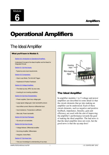
Module6AmplifiersOperational AmplifiersThe Ideal AmplifierWhat you’ll learn in Module 6.Section 6.0. Introduction to Operational Amplifiers.Understand Concept of the Ideal Amplifier and the Need forIntegrated Circuits.Section 6.1 Op Amp Inputs. Typical op amp input requirements.Section 6.2 Comparators. Open Loop Mode, The Schmitt Trigger. Hysteresis & Positive Feedback.Section 6.3 Voltage Amplifiers. The ideal op amp, NFB, Op amp rules.The Ideal Amplifier Inverting & non-inverting amplifiers.Section 6.4 Op Amp Characteristics.In amplifier modules 1 to 5 voltage and poweramplifiers are described in some detail so thatthe circuit elements that go into making anamplifier can be understood. Each of thesecircuit elements, such as negative and positivefeedback, impedance, linearity, gain andefficiency are used with the aim of improvingthe amplifier’s performance towards the goalof making the ideal amplifier. The bad news isthat the ideal amplifier does not exist, but thegood news is that the op amp does! Power supplies, Open loop voltage gain. Large signal voltage gain, Gain bandwidth product. Input offset current, Maximum differential input. Input resistance, Temperature coefficient. Slew rate, Power bandwidth.Section 6.5 Op Amp Packages. Op amp pin out examples.Section 6.6 Op Amp Circuits. Voltage follower, Differential amplifier. Summing Amplifier, Differentiator. Integrator, Active filters.Section 6.7 Op Amps Quiz. Test your knowledge & understanding of op amps.AAMPLIFIERS MODULE 06.PDF1 E. COATES 2007 -2012
www.learnabout-electronics.orgAmplifiers Module 6The ideal amplifier should: Have an infinitely wide bandwidth. Have an infinitely high gain available that can be easily controlled. Be ideally linear, with no distortion. Generate no noise (have an infinitely high signal to noise ratio). Be easily convertible to perform different amplifier functions. Be cheap.All of the above is what the op-amp does, or at least comes pretty close to.Early Op ampsAmplifiers with gain controlled by negative feedback were first thought of in the 1930s as a way ofcreating amplifiers for the telephone system that could have a controllable and reliable gain, butbecame operational amplifiers when they were adopted by designers of analogue computers,because of their ability to perform accurate mathematical operations, such as adding, subtracting,integration and differentiation.Op amp ICsOperational amplifiers can still built from discrete components but with the introduction of siliconplanar technologies and integrated circuits their performance improved and both size and costreduced dramatically, and although computing has practically all moved from analogue circuitry todigital, the op amp had become so useful in so many circuits that deal with real (analogue)quantities such as sound, light, heat and motion, that the op amp is now a widely varied andindispensable part of electronics equipment.This module will discuss the basic properties of op amps and comparators, and how their integratedcircuit versions can be manipulated to make simple circuits that provide so many vital functions inelectronics.AMPLIFIERS MODULE 06.PDF2 E. COATES 2007 -2012
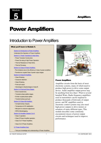
www.learnabout-electronics.orgAmplifiers Module 6Module 6.1Op Amp InputsWhat you’ll learn in Module 6.1After studying this section, you shouldbe able to:Recognise typical forms of op amp circuitsymbols.Fig. 6.1.1 Op Amp Circuit SymbolUnderstand the need for single & dual powersupplies.Op Amp Circuit SymbolUnderstand typical operating requirements.The circuit symbol for an op amp is basically thestandard triangle symbol for an amplifier. Mainconnections such as the inverting ( ) and noninverting inputs and the output are shown, but often,other connections are not. A typical op amp symbolis shown in Fig. 6.1.1. Note however, that manycircuit diagrams do not show the DC supplyconnections. High gain & negative Feedback. Differential inputs. Constant current sourcing. Common Mode Rejection, CMRR. Offset null.Dual Power SuppliesAn op amp needs a minimum of five connections as shown in Fig 6.1.1; as well as the two inputsand one output there are two power supply connections. These may be labelled Vs and -Vsindicating that the IC needs both positive and negative supplies. These will often be in the range of 5V to 15V for the positive supply and -5V to -15V for the negative supply. This dual supplyarrangement allows for the output voltage to swing both above and below zero volts, and also givesan output of 0V when there is no voltage difference between the two inputs.Single Supply Op AmpsA growing number of op amps are available however, that use a single supply, labelled V and Gndor 0V. This is a useful arrangement for many portable and mobile applications where dual positiveand negative supplies are not readily available, for example in automobile applications.High Gain Negative Feedback DC AmplifierOp amps are basically negative feedback (NFB) DC amplifiers. The op amp has a very large gain,the output can be hundreds of thousands times larger than the input. This huge gain however, isreduced using negative feedback to produce a circuit whose gain is stable and independent of thesemiconductor characteristics.Op amps are also always DC coupled, unlike an amplifier using discrete components where it ispossible to include AC components such as capacitors and inductors, in a tiny integrated circuit it isnot possible to fabricate AC components large enough to be useful at audio frequencies, thereforean op amp MUST be a DC amplifier.AMPLIFIERS MODULE 06.PDF3 E. COATES 2007 -2012
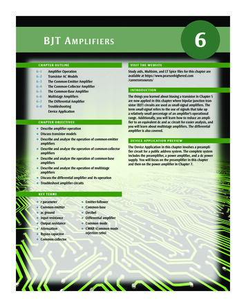
www.learnabout-electronics.orgAmplifiers Module 6One advantage of using DC (directly coupled or direct current) amplifiers is that their bandwidthextends right down to 0Hz, making them suitable for many control and measurement applicationswhere the op amp’s ability to produce a DC output, relative to the difference between two DC inputquantities is extremely valuable. The problem with directly coupled amplifiers however, is theirtendency to drift. That is for the DC voltages present in the circuit to change, especially withchanges in temperature. Because the op amp has a very high gain, it only takes a tiny change involtage at the input to produce a large voltage change at the output. Because of this, op amp inputcircuits are designed around a differential amplifier, also called an emitter-coupled amplifier or along tailed pair, which provides the op amps two (inverting and non-inverting) inputs and also hasthe ability to cancel out voltage drift.Difference AmplifierThe Op amp’s basic operation is that of a differenceamplifier, producing a voltage output that is proportionalto the voltage difference at its two inputs. These inputs,labelled - (the inverting input) and (the non-invertinginput) form the inputs of an emitter coupled amplifier, abasic example of which is shown in Fig. 6.1.2, it consistsof a pair of matched transistors Tr1 and Tr2, which sharethe same emitter resistor RE.Suppose that one of the inputs (b) is held at a fixedvoltage, providing a suitable base bias to make Tr2conduct. If a signal is now applied to input (a), each timeFig.6.1.2 Emitter Coupled Amplifierthe signal voltage rises Tr1 conduction increases, itscollector voltage falls and its emitter voltage (the voltageacross the shared RE) rises. This rise also causes a rise in the emitter voltage of Tr2. As the base ofTr2 is fixed, the base-emitter voltage (VBE) of Tr2 decreases and reduces the current through Tr2.This causes the voltage at Tr2 collector to rise, making the signal at output C rise in anti-phase tothe output at D.Provided that the transistors are ideally matched, and there are no other factors to cause differencesbetween the conduction in each half of the circuit, the rise in current due to Tr1 conducting iscancelled out by the fall in current through Tr2, and the voltage across RE should not change. Inpractice the change would only be a few millivolts.Common Mode SignalsIf two identical signals are applied to each input, two possibilities may be considered:1. The signals at each input are identical and in anti-phase with each other.2. The signals at each input are identical and in phase with each other.Condition 1 is called a differential input as there is a difference produced by the anti7#45;phasesignals. In this case the two amplified signals produced at the two outputs will be an amplifieddifference between the two signals, but as the output signals are in anti-phase with each other, as onsignal voltage rises the other signal voltage falls and the resulting signal between outputs C and Dwill be twice the amplitude of either single output.Condition 2 has both input signals in phase and so is called a common mode input. The outputs Cand D are also in phase, both rising and falling together. Therefore the difference between outputs Cand D is zero. The differential amplifier therefore can be said to amplify a differential input, but toAMPLIFIERS MODULE 06.PDF4 E. COATES 2007 -2012
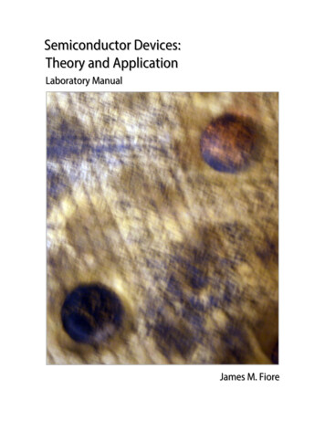
www.learnabout-electronics.orgAmplifiers Module 6reject, or to be immune to, a common mode input. This ideal rejection of common mode signalsdoes not quite occur in practice as there are bound to be some slight differences between the gainsbetween each of the two inputs and their respective outputs, even when, in an integrated circuit theyare fabricated on the same piece of silicon. However, common mode signals that cause both Tr1 andTr2 emitter currents to rise and fall in unison, this will set up changing voltage across the sharedemitter resistor RE and because there is no decoupling across RE negative feedback will occur,causing the common mode gain of the amplifier to be reduced. This common mode feedback can beused to improve common mode rejection if a large value for RE is used.Constant Current SourceRather than relying solely on the negative feedbackproduced by RE to improve common mode rejection inintegrated circuits, most op amp ICs replace RE in theemitter coupled amplifier with a constant current sourceas shown in Fig. 6.1.3. This circuit is much moreefficient at preventing variations in the shared emittercurrent of Tr1 and Tr2 that are due to common modesignals. The base of Tr3 is biased at relatively fixedvoltage, in this case by a potential divider formed by R4and the three forward biased diodes D1, D2 and D3, butother arrangements, usually consisting of somecombination of diodes or zener diodes and resistors canbe used.In the presence of a common mode signal, the collectoremitter current through Tr3 will try to vary; any increasein this current would increase the voltage across R3, andFig.6.1.3 Constant Current Sourceany decrease would reduce it. However because the basevoltage of Tr3 is held at a steady voltage, an increase incollector-emitter current will increase the emitter voltage and therefore reduce V BE. This will reducethe conduction of Tr3 and reduce the collector-emitter current, back to its original value. A decreasein Tr3 collector-emitter current would similarly increase VBE and increase conduction of Tr3 untilthe current returned to normal once again. Including a constant current source in the emitter circuitof the differential amplifier makes the rejection of common mode signals very efficient.Notice that in the circuit shown in Fig. 6.1.3 only a single output from Tr2 collector is used toproduce a single amplified voltage that is proportional to the difference between inputs a and b, andis almost entirely unaffected by changes common to a and b. There are op amps available that usetwo outputs, but single output op amps are far more numerous.Common Mode Rejection Ratio (CMRR)Ideally the op amp output responds only to differential signals, but in practice, even when the inputsare at exactly the same potential, and the output should be at zero volts, some small output potentialwill be present. This is caused by inevitable small differences in gain between the inverting and thenon-inverting inputs. The op amp therefore has some gain to common mode signals, which isindicated by the parameter Common Mode Voltage Gain (AVCM) and the ratio between this and theDifferential Voltage Gain (AVD) is indicated in the main op amp parameters by the Common ModeRejection Ratio CMRR. Because this ratio is normally a very large number it is often quoted indeciBels.AMPLIFIERS MODULE 06.PDF5 E. COATES 2007 -2012
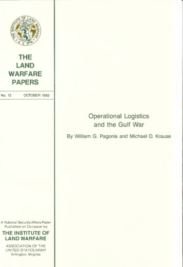
www.learnabout-electronics.orgAmplifiers Module 6A reason that the CMRR is an important parameter is that when an op amp is used, as they oftenare, in circuits involving measurement, some error will be present, for example when measuring thedifference between two very small voltages, this error is amplified along with the true differentialvoltage, so making any measurement inaccurate.In some modes of operation common mode signals are not produced, such as when the op amp isused as an inverting amplifier, and the non-inverting input is grounded. Then the only time theinputs are the same is when they are both zero.Offset NullIf common mode signals are to be avoided, the gain from eachof the inputs must match as closely as possible. To produce opamps with minimal common mode gain, manufacturers usevarious techniques such fabricating extra resistors to control thegain form each input within the chip, these may then be removedas required, by selectively blowing fuses to remove individualresistors from one or other channel to balance the input gains.Another, more accurate technique with tiny resistors embeddedin the silicon chip, is to use lasers to trim the width of theresistors to alter their resistance during manufacture and testingprocess.Fig.6.1.4 Offset Null AdjustmentAlthough modern op amps can be made to have very low offset voltages many op amps provide twoextra pins for additional external offset nulling. A typical offset null arrangement is shown in Fig.6.1.4. A potentiometer is connected between the two offset null pins with the potentiometer wiperconnected to the negative power supply. The inputs are both connected to ground and with poweron and the IC running at ambient temperature the pot is adjusted to make the output voltage 0V.Note that it is quite common for the offset null potentiometer, although present in the actual circuit,to be omitted from the circuit schematic diagram, as once adjusted during manufacture it is notconsidered to play any further part in the circuit’s basic operation.Because such small voltages are involved, the adjustment can be quite sensitive and wherenecessary the 10K potentiometer could be replaced by a 1K with 4K7 resistors fitted between eachend of the potentiometer track and the offset null pins of the IC.AMPLIFIERS MODULE 06.PDF6 E. COATES 2007 -2012
www.learnabout-electronics.orgAmplifiers Module 6Module 6.2ComparatorsUsing the Op Amp’s Open LoopGainWhat you’ll learn in Module 6.2After studying this section, you should be able to:Describe how Op Amps can be used asComparators. Uses and Limitations.Understand Hysterisis as applied to Comparators. Switching speed. Effects of noise on switching.Describe the operation of a Schmitt TriggerComparator. The effect of positive feedback. The control of Hysteresis.Understand typical Technologies used inDedicated Comparator ICs. Hysteresis and reference voltage. Low Power v Switching Speed. Typical Comparator Applications.The output of an op amp can swing positive andnegative to a maximum voltage close to thesupply rail potentials. For example, themaximum output voltage for the popular 741 opamp, when connected to a 18V supply is 15VBecause the open loop gain of an op amp isextremely high however, typically 10,000 toone million, means that without negativefeedback, any input that creates a difference involtage between the two input pins greater than 150µV will amplified 100,000 or more timesand drive the output into saturation; the outputappears to be ‘stuck’ either its maximum orminimum value. Using the maximum open loopgain in this way can be useful when eitherdealing with extremely small (and lowfrequency or DC) inputs in instrumentation ormedical applications, or for comparing twovoltages, using the op amp as a comparator. Inthis mode the output will go to either amaximum high or minimum low leveldepending on whether one input is just a fewmicro volts higher or lower than a referencevoltage applied to the other input.The Op Amp as a ComparatorBasic op amp types such as the 741 will performadequately as comparators in simple circuits, such as atemperature controlled switch that is required to switchon or off a circuit when the input voltage from atemperature sensor is higher or lower than a presetreference value. In Fig. 6.6.1 a reference voltage isapplied to the non-inverting input, whilst a variablevoltage is applied to the inverting input. Whenever thevoltage applied to pin 2 is higher than the referencevoltage on pin 3 the output will be at a low voltage, onlyslightly higher than Vs and if pin 2 is at a lower voltagethan pin 3, the output voltage will be high, slightly lessthan Vs.Fig. 6.6.1 Using an Op Ampas a ComparatorAMPLIFIERS MODULE 06.PDF7 E. COATES 2007 -2012
www.learnabout-electronics.orgAmplifiers Module 6However standard op amps are designed for low power amplification purposes and if they aredriven into, then out of saturation, it takes some time for the output voltage to recover and for the opamp to begin operating in a linear manner once more.Op amps designed as amplifiers are not particularly suited to use as comparators especially wherethe input signals are changing rapidly in such applications as audio level sensors or analogue todigital converters. Another problem with the basic comparator arrangement illustrated in Fig 6.6.1that is addressed by op amps specially designed as comparators rather than amplifiers, is that ofnoise. If there is a significant amount of noise on the input signal, especially when the input signalvoltage is close to the reference voltage level, the high frequency voltage variations caused by therandom nature of the noise will make the input signal voltage higher and lower than the referencevoltage in rapid succession, causing the output to momentarily oscillate between its maximum andminimum voltage levels. However this problem is overcome in many dedicated comparators byapplying hysteresis.HysteresisThis refers, in comparators and switching circuits, to the property of the output in switching to itshigh or low states at different input values. If a comparator switched its output at a single inputvoltage level as explained in the previous paragraph, or if the difference in the two levels providedby the comparator’s hysteresis is not wide enough, the switching from one of the two outputconditions to the other could be very uncertain. Hysteresis can be applied to the op amp comparatorand adjusted for a suitable hysteresis gap by using positive feedback in a circuit arrangement calledthe Schmitt Trigger.The Schmitt TriggerThe Schmitt Trigger circuit shown in Fig. 6.6.2is an inverting comparator based on the LM339quad comparator IC from Texas Instrumentswith its reference value applied to the noninverting input by the potential divider R1 andR2. This sets the reference voltage at half ofthe 5V single supply. R3 is a pull-up resistor,which is used on the LM339 as this comparatorhas an open collector output, that is an outputstage whose collector does not have an internalload resistor connected to supply. The reasonfor this is that it allows the output to have awider range of DC voltages, rather than justbeing able to vary between supply and ground.Positive FeedbackFig. 6.6.2 The Op Amp Schmitt TriggerThe resistor R4, connected between output andpin 5 (the non-inverting input) provides positive feedback to speed up output switching as follows.Suppose the voltage Vin on pin 4 is rising towards the reference voltage Vref on pin 5 and the outputon pin 2 is high. Once Vin is slightly higher than Vref the output will start to fall towards 0V. Aproportion of this fall in voltage is fed via R4 to pin 5 and so begins to reduce Vref increasing thedifference between Vref and Vin. This causes the output to fall faster and because this fall iscontinually fed back to Vref the fall in the output voltage accelerates, causing a very rapid fall tozero volts.AMPLIFIERS MODULE 06.PDF8 E. COATES 2007 -2012
www.learnabout-electronics.orgAmplifiers Module 6A similar action occurs when a high voltage on pin 4 falls to a lower value than pin 5, ensuring veryfast output switching. There is however, another action taking place; it was mentioned in theprevious paragraph that a fall in the output voltage is fed back via R4 and causes a fall in V ref andlikewise a rising output voltage will cause a rise in Vref. Therefore Vref changes depending onwhether the output voltage is high or low. Some hysteresis has been introduced into the circuitoperation.Controlling the HysteresisThe centre point between the hysteresison and off levels is Vref controlled by thechoice of values of R1 and R2. Theamount of hysteresis (the differencebetween the switch on and switch offpoints) is controlled by the value R4.The reason for this can be seen from Fig.6.6.3, which shows that because theoutput end of R4 is effectively connectedto either 5V (when the output is high,or to 0V when the output is low, it iseither in parallel with R1 (high output)or with R2 (low output), and so changesthe voltage at the centre of the R1/R2potential divider accordingly. Thereforeby appropriately choosing the value ofR4, the amount of hysteresis can bechosen to accommodate variousanticipated levels of noise.Fig. 6.6.3 The Effect of R4 on HysteresisDedicated Comparator ICsFor high speed comparisons many dedicated comparator op amps are also available that will changetheir output state in less than 1µs. However, as is general with most electronic circuits, the faster theoutputs change, the more power is consumed. Comparators of various speeds and different powerconsumption figures are available so that the ideal IC for a given application can be used whetherpower consumption or speed is more important.Using methods similar in effect to those described above, high speed comparator integrated circuitswith built in hysteresis are available such as the LTC1541 from Linear Technology, which has abuilt in hysteresis property of 2.25mV to allow for noise on the input signal.Comparator ICs are also available that have variable hysteresis to cope with different amounts ofnoise, and a built in precision reference voltage. Some comparators, such as the LMP7300 fromTexas Instruments can also operate from very low single supply voltages and at extremely lowcurrents. This makes them ideal for such applications as low battery voltage detectors in portableequipment.AMPLIFIERS MODULE 06.PDF9 E. COATES 2007 -2012
www.learnabout-electronics.orgAmplifiers Module 6Module 6.3Op Amp Voltage AmplifiersWhat you’ll learn in Module 6.3After studying this section, you should beable to:Compare ideal and practical op amps.Understand the operation op amps The use of negative feedback. Current rule for op amps. Voltage rule for op amps.Fig. 6.7.1 The Ideal Op Amp The inverting voltage amplifier. The non-inverting voltage amplifier.The Ideal Op AmpAlthough the ideal op amp does not exist in reality, a real (practical) op amp comes reasonablyclose to achieving the ideal. An ideal amplifier should, in addition to other desirable parameters,have at least an infinitely high input impedance, an output impedance of zero ohms, an infinitelyhigh gain and an infinitely wide bandwidth. Table 1 compares some basic parameters of sometypical real (practical) op amps with the ‘ideal’ model:Table 1: The Ideal Amplifier v The Practical Op AmpParameterInput Impedance(ZIN)Input Bias Current(IIN)Large SignalVoltage Gain (AV)Output Impedance(ZOUT)The IdealAmplifier741TLC271LMC660Infinity.2MΩ1TΩ 1TΩZero.80nA60pA0.002pAInfinity0Ω316 to 200,000 5,000 to 46,000 (74dB 40,000 to 990,000(50dB to 106dB)to 93dB) minimum(92dB to 126dB)Depends on gain and feedback but typically less than 100Ω tomore than 1KΩNegative FeedbackThere are two basic methods of connection for op amp voltage amplifiers, making the op amp intoan inverting or a non-inverting voltage amplifier. In each case, the voltage gain of the amplifier isset simply by the ratio of two resistors. Using a very high gain amplifier and applying negativefeedback produces a very stable amplifier whose gain is virtually independent of changes intemperature or variations in semiconductor characteristics. Just as in the discrete componentamplifiers described in Module 3, the negative feedback also reduces distortion and noise inaddition to increasing the bandwidth of the amplifier.AMPLIFIERS MODULE 06.PDF10 E. COATES 2007 -2012
www.learnabout-electronics.orgAmplifiers Module 6Op Amp RulesIdeal op amps, when used with feedback, operate in a way that can be predicted by a couple of basicrules, often called "Golden Rules"Rule 1. The Voltage Rule.The op amp output will change as necessary to keep the two input voltages identical. If any inputsignal or voltage tries to make the inputs different potentials, the op amp output will change in theopposite polarity to the input and, via the feedback loop, keep the difference between the two inputsat 0V.Rule 2. The Current Rule.Because the input impedance is infinitely high, no current can flow into either input.These rules used in relation to the ideal op amp can be used to make the operation of the two mainvoltage amplifier circuits easier to understand. The small differences between ideal and practical opamps can be temporarily ignored.The Inverting AmplifierFig. 6.7.3 shows the inverting amplifier, in this configuration the signal input is applied to theinverting ( ) input to produce an anti-phase output signal whose amplitude is Vin x Avcl where Avclis the closed loop gain of the op amp.Negative feedback is used to reduce the op amp’s very high maximum gain to the required level.The closed loop gain (Avcl) is set simply by the ratio of R f to RinHow the Inverting Amplifier WorksBy applying the two rules to the ideal op ampshown in Fig. 6.7.3a it can be assumed that:Pin 3 is at 0V, as it is connected to ground, so pin2 will also be at 0V (Rule 1)Therefore Rin and Rf are effectively connected inseries between Vin and Vout with pin 2 between thetwo resistors held at 0VNo current can flow into pin 2 (Rule 2) so thecurrent flowing into Vin cannot be flowing into theop amp, therefore it must be flowing through RfThe diagram in Fig. 6.7.3b shows that in effect Rinand Rf are two resistors connected in seriesbetween Vin and Vin with Pin 2 at 0V.Although pin 2 is not actually connected toground, pin 3 is connected to ground and rule 1 ismaking pin 2 0V, this effect of making a point thatis not actually connected to ground maintain a zerovoltage is called ‘virtual earth’ (or virtual ground).AMPLIFIERS MODULE 06.PDF11Fig.6.7.3 The InvertingAmplifier E. COATES 2007 -2012
www.learnabout-electronics.orgAmplifiers Module 6Any input current (Iin) therefore flows directly from the input, via Rin and Rf to the output, with Rinand Rf forming a potential divider between the opposite polarity voltages V in and Vout with pin 2 at0V.The current through a series resistor circuit is the same for each resistor, so the input voltage V inwill be proportional to the resistance of Rin, and the voltage across Rf will be proportional theresistance of RfNotice that because Rf is effectively connected between the output terminal and virtual earth (0V)the voltage across Rf is also equal to Vout. This makes Rf / Rin equal to Vout / Vin (the gain of theamplifier) and therefore the closed loop gain of the inverting op amp voltage amplifier (A vcl) isgiven by the equation:Notice that the formula only tells you the ratio of the resistor and not their actual values. Fortunatelyin audio amplifiers the values are not too critical, usually keeping the resistor values between about10K and 100K is OK. However it is good to try and keep Rin as high a resistance as possible, andalso in a practical amplifier, rather that grounding the non-inverting input directly it should begrounded by a resistor with the same value as Rin to keep the (tiny) input currents equal. This givesa better chance of the output voltage being zero volts (or close to it) when the input is zero volts.The Non-inverting AmplifierIn the non-inverting amplifier illustrated in Fig. 6.7.4a theinput is applied to the non-inverting input (pin 3) while thenegative feedback resistor (Rf) together with R1 set theclosed loop gain of the amplifier.The input and output signals are now in phase, whichchanges the circuit operation. As shown in Fig. 6.7.4b, thecircuit does not have a virtual earth point, but the bottomend of R1 is connected to ground, which means that pin 2will follow the varying input voltage Vin on pin 3 (Rule 1).Rf and R1 now form a potential divider between V out and0V and just like the inverting amplifier, no current willflow into pin 2 (Rule 2) so the voltages across R1 and R fwill be proportional to the individual resistances. The ratioof the resistances, and the ratio of Vout to Vin i.e. the closedloop gain is given by the standard potential divider formula(Rf R1) / R1.AMPLIFIERS MODULE 06.PDF12Fig.6.7.4 The Non-Inverting Amplifier E. COATES 2007 -2012
www.learnabout-electronics.orgAmplifiers Module 6Module 6.4Op Amp CharacteristicsWhat you’ll learn in Module 6.4After studying this section, you should beable to:Understand commonly published op ampcharacteristics. Power suppliy requirements. Open loop voltage gain. Large signal voltage gain. Gain bandwidth product. Input offset current. Maximum differential input. Input resistance, Temperature coefficient. Slew rate, Power bandwidth.Supply VoltageTwo types of suppl
Because of this, op amp input circuits are designed around a differential amplifier, also called an emitter-coupled amplifier or a long tailed pair, which provides the op amps two (inverting and non-inverting) inputs and also has the ability to cancel out voltage drift. Difference Amplifier The