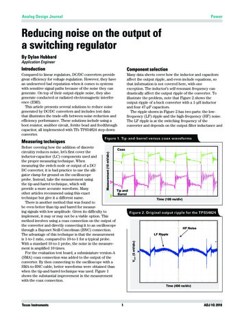
Transcription
Analog Design JournalPowerReducing noise on the output ofa switching regulatorBy Dylan HubbardApplication EngineerIntroductionComponent selectionCompared to linear regulators, DC/DC converters providegreat efficiency for voltage regulation. However, they havean undeserved bad reputation when it comes to systemswith sensitive signal paths because of the noise they cangenerate. On top of their output-ripple noise, they alsogenerate conducted or radiated electromagnetic interference (EMI).This article presents several solutions to reduce noisegenerated by DC/DC converters and includes test datathat illustrates the trade-offs between noise reduction andefficiency performance. These solutions include using aboot resistor, snubber circuit, ferrite bead and feedthroughcapacitor, all implemented with TI’s TPS54824 step-downconverter.Many data sheets cover how the inductor and capacitorsaffect the output ripple, and even include equations, sothat information is not covered here, with oneexception. The inductor’s self-resonant frequency candrastically affect the output ripple of the converter. Toillustrate the problem, note that Figure 2 shows theoutput ripple of a buck converter with a 1-µH inductorand four 47-µF capacitors.The ripple shown in Figure 2 has two parts: the lowfrequency (LF) ripple and the high-frequency (HF) noise.The LF ripple is at the switching frequency of theconverter and depends on the output filter inductance andMeasuring techniquesFigure 1. Tip-and-barrel versus coax waveformsVOUT (5 mV/div)Measurement (10 mV/div)Before covering how the addition of discreteCoaxcircuitry reduces noise, let’s first cover theinductor-capacitor (LC) components used andthe proper measuring technique. Whenmeasuring the switch node or output of a DC/DC converter, it is bad practice to use the alligator clamp for ground on the oscilloscopeprobe. Instead, take the measurement using2the tip-and-barrel technique, which willprovide a more accurate waveform. ManyTip andother articles recommend using this exactBarrel4technique but give it a different name.Time (100 ns/div)There is another method that was found tobe even better than tip and barrel for measuring signals with low amplitude. Given its difficulty toFigure 2. Original output ripple for the TPS54824implement, it may or may not be a viable option. Thismethod involves using a coax connection on the output ofthe converter and directly connecting it to an oscilloscopeHF Noisethrough a Bayonet Neill-Concelman (BNC) connection.LF RippleThe advantage of this technique is that the measurementis 1-to-1 ratio, compared to 10-to-1 for a typical probe.With a standard 10-to-1 probe, the noise in the measurement is amplified 10 times.For the evaluation test board, a subminiature version-A(SMA) coax connection was added to the output of theconverter. By then connecting to the oscilloscope with aSMA-to-BNC cable, better waveforms were obtained thanwhen the tip-and-barrel technique was used. Figure 1shows the substantial improvement in the measurementwith the coax connection.Time (400 ns/div)Texas Instruments1ADJ 1Q 2018
Analog Design JournalPowercapacitance. The HF noise comes from the coupling of theswitch node’s high-frequency ringing through the parasiticcapacitance of the inductor (the oscilloscope must haveenough bandwidth to capture this, typically 200 MHz).HF noise can be very harmful to systems with sensitivesignal chains. All integrated circuits (ICs) have a powersupply rejection ratio (PSRR) that enables the VCC pin toreject a certain amount of noise coming from that powerrail. At higher frequencies, this PSRR value decreases,allowing the HF noise to couple through more easily. That’spotentially 20 mVpp of noise getting into the signal chain.This is where it becomes critical to take a close look atchoosing the inductor. To account for high-frequencynoise, an inductor was selected with a higher self-resonantfrequency to minimize the parasitic capacitance at thefrequency of the noise. Figure 3 shows the resultingoutput ripple.The inductor value was the same at 1 µH and thecurrent ratings were similar as well. But increasing theself-resonant frequency reduced the output ripple by over50%. The important trade-off to this improved performance is the size of the inductor. The original inductorwas 6 by 6 by 3 mm and the inductor with higher selfresonant frequency was 8 by 8 by 7 mm. An inductor thissize can take up too much space in many applications, soadditional solutions must be considered to reduce noise.VOUT (5 mV/div)Figure 3. Output ripple with an inductorwith a high self-resonant frequencyTime (400 ns/div)Switch Node (10 V/div)Figure 4. Original switch-nodewaveform for the TPS54824Boot resistorA boot resistor is the easiest and most conservative solution that can reduce noise when it comes to spatial densityand efficiency. Placing this resistor in series with the bootstrap capacitor provides a charge to the gate driver of thehigh-side metal-oxide semiconductor field-effect transistor(MOSFET). The purpose of the resistor is to slow theturn-on time of the high-side MOSFET by impeding thecurrent charging the gate, which will reduce the initialpeak amplitude of the switch-node ringing.Figure 4 shows the switch-node waveform of the testboard with the original components and no addedcircuitry. Figure 5 shows the effects of adding a 3-Ω bootresistor, which reduced the maximum voltage at theswitch node by roughly 3 V. The resistor value is proportional to the reduction in ringing. However, too muchresistance can negatively affect the functionality of theDC/DC converter. Most data sheets give a range of valuesfor the boot resistor that are safe to use without starvingthe gate.Time (10 ns/div)Switch Node (10 V/div)Figure 5. Switch-node waveformwith a boot resistorTime (10 ns/div)Texas Instruments2ADJ 1Q 2018
Analog Design JournalPowerReducing the ringing also reduces the output ripplebecause the high-frequency noise correlates to the ringing.Figure 6 shows the output ripple with the boot resistoradded.Compared to Figure 2, Figure 6 shows a reduction inthe resulting output ripple by roughly 8 mV. Again, thegreater the resistance, the lower the ripple.Not only is the boot resistor helping with output-ripplereduction, but it also helps with radiated EMI reduction.Lowering the initial peak of the ringing reduces the magnitude of the EMI created by the switching. To explore thebenefits of EMI reduction for a real-world applicationrequiring low noise, see Reference 1.VOUT (5 mV/div)Figure 6. Output ripple with boot resistorSnubber circuitA snubber circuit contains a resistor and capacitor thatshould dampen the switch-node ringing by absorbing theenergy stored in the parasitic elements of the MOSFETsand printed circuit board (PCB). For more detail aboutdesigning a snubber circuit, see Reference 2.The test board used a 330-pF CSNUB and an 8.2-Ω RSNUB.The switch node connects to ground through these twopassive components. Figure 7 shows the dampening of theswitch-node ringing and Figure 8 shows the resultingoutput ripple.Compared to Figure 4, the reduced amount of ringingresults in a 6-mV output-ripple reduction. With thesnubber circuit, the amount of dampening depends on thesize of the capacitor. The more capacitance, the more itdampens, with the trade-off of more power loss.Using a snubber circuit also works for both EMI andoutput-ripple reduction. Unlike a boot resistor, a snubbercircuit doesn’t reduce the initial peak as much as itreduces the amount of ringing.Take care when selecting the package size for the resistor-capacitor (RC) components because the powerrating decreases with size and the resistor needs to beable to handle the power it dissipates. A snubber circuitcan be combined with a boot resistor for noise reductionwith minimal efficiency loss. To learn a little more aboutthe benefits of both techniques, see the TI Training video(Reference 3), which addresses the flexibility gained byusing a discrete DC/DC converter rather than a powermodule.Time (400 ns/div)Switch Node (10 V/div)Figure 7. Switch-node waveformwith a snubberTime (10 ns/div)VOUT (5 mV/div)Figure 8. Output ripple with a snubberTime (400 ns/div)Texas Instruments3ADJ 1Q 2018
Analog Design JournalFerrite beadsPowerFigure 9. Example of impedance versusVOUT (5 mV/div)Impedance (Ω)Ferrite beads are common in noise-sensitive systems.frequency for a ferrite bead*They are popular for “soaking” up conducted EMIdue to their AC resistance at high frequencies, which1000dissipates the noise as heat. The problem is that itmay be difficult to select the proper ferrite bead forsome applications because several parameters canaffect their performance.To determine the best working frequency of aZferrite bead, look for a plot with impedance versus100frequency like the one shown in Figure 9. For simulation purposes, an inductor, AC resistor and capacitorin parallel can model this impedance characteristic inits simplest form.XLUnfortunately, the plot for impedance versusRfrequency changes significantly with current level10through the ferrite bead, which increases the difficulty of selecting the right bead for the job. Somecompanies (like Wurth Electronics) provide a simulation tool on their Web site where the current can beadjusted to see the change in the AC resistance orimpedance curves. For testing, the bead part numberselected was 74279221100, which will handle the 8-A11101001000maximum output current of the TPS54824 buckFrequency (MHz)converter. When the ferrite bead was added,compensation adjustments were also made to make*Source: With permission from Wurth Electronics data sheet.the buck stable. This adjustment varies with thecharacteristics of the ferrite bead and the type of buckconverter. Figure 10 shows the output ripple with theFigure 10. Output ripple with ferrite beadferrite bead placed at the output of the DC/DC converter.In Figure 10, the ferrite bead did not decrease the highfrequency ripple by that much, mostly because the highcurrent requirement resulted in a lower AC resistance atthe desired frequency. The low-frequency ripple isreduced, but that’s due to the ferrite bead being primarilyinductive at the switching frequency of the converter.When a single-voltage supply is used to power multipleloads, instead of using one ferrite bead, multiple ferritebeads (one at each load) can improve filtering performance by reducing the current through each bead. Thismakes it much easier to find a bead that has a higher ACresistance at the frequency to be eliminated.Time (400 ns/div)Texas Instruments4ADJ 1Q 2018
Analog Design JournalPowerFeedthrough capacitorFigure 11. Output ripple with afeedthrough capacitorVOUT (5 mV/div)A feedthrough capacitor performs well when filtering awide range of high frequencies because the additionalthird terminal reduces the equivalent series inductance(ESL) compared to a typical ceramic capacitor. To maximize noise reduction, choose a capacitor with the highestinsertion loss at the frequency of the noise; for the testboard, it was the frequency of the switch-node ringing.Figure 11 shows the output ripple with a feedthroughcapacitor implemented on the board.Note in Figure 11 that the feedthrough capacitorreduced both the high-frequency noise and low-frequencyripple because it filters out the low-frequency ripple like astandard capacitor. There is also more insertion loss athigher frequencies than with a standard ceramic capacitor.See Reference 4 for additional information about designingwith chip feedthrough capacitors.Power lossPower loss can be an important factorwhen trying to select the right noise filterfor a DC/DC converter. Power-loss datawas gathered and plotted for each technique implemented to reduce noise asshown in Figure 12. The test parameterswere VIN 12 V, VOUT 1.8 V and a loadcurrent range from 0 to 8 A.Time (400 ns/div)Figure 12. Power loss data2.52ConclusionPower Loss (W)This article provides a foundation for1.5designing a DC/DC switching regulator forlow-noise systems. Most techniques toreduce noise do require additionalcomponents.1The most effective solution to reducehigh-frequency noise involves lookingdeeper into the characteristics of the0.5output inductor, a fundamental componentin a buck converter. Using an inductor witha high self-resonant frequency may seemobvious, but this parameter is easy0to overlook.0When it isn’t possible to have an inductor with a high self-resonant frequency, thedirect solution may be to use the standardcircuit recommended in the data sheet and add a simpleboot resistor, snubber circuit, ferrite bead or feedthroughcapacitor.OriginalBoot ResistorSnubberFerrite BeadFeedthroughCapacitor134Load Current (A)56783. Pat Hunter, “DC/DC Converter Flexibility EnablesAdding Noise Reduction Circuitry,” Texas Instrumentstraining video, October 16, 2017.4. “Basics of Noise Countermeasures [Lesson 5] Chip 3terminal capacitors,” Murata noise suppression filterroom, September 28, 2011.References1. “Multi-Rail Power Reference Design for Eliminating EMIEffect in High Performance DAQ Systems,” TexasInstruments reference design (TIDA-01054),18 September, 2017.2. John Betten, “Power Tips: Calculate an R-C snubber inseven steps,” Texas Instruments E2E Communityblog post, May 5, 2016.Texas Instruments2Related Web sitesProduct information:TPS548245ADJ 1Q 2018
Analog Design JournalTI Worldwide Technical SupportTI SupportThank you for your business. Find the answer to your support need or get intouch with our support center chnical support forumsSearch through millions of technical questions and answers at TI’s E2E Community (engineer-to-engineer) :http://e2e.ti.com/group/jp/TI TrainingFrom technology fundamentals to advanced implementation, we offeron-demand and live training to help bring your next-generation designs to life.Get started now l/cn/docs/gencontent.tsp?contentId 71968Japan:https://training.ti.com/jpImportant Notice: The products and services of Texas Instruments Incorporated and itssubsidiaries described herein are sold subject to TI’s standard terms and conditions of sale.Customers are advised to obtain the most current and complete information about TI products andservices before placing orders. TI assumes no liability for applications assistance, customer’sapplications or product designs, software performance, or infringement of patents. The publicationof information regarding any other company’s products or services does not constitute TI’s approval,warranty or endorsement thereof.A011617E2E is a trademark of Texas Instruments. Allother trademarks are the property of theirrespective owners. 2018 Texas Instruments Incorporated.All rights reserved.Texas InstrumentsSLYT7406ADJ 1Q 2018
IMPORTANT NOTICE FOR TI DESIGN INFORMATION AND RESOURCESTexas Instruments Incorporated (‘TI”) technical, application or other design advice, services or information, including, but not limited to,reference designs and materials relating to evaluation modules, (collectively, “TI Resources”) are intended to assist designers who aredeveloping applications that incorporate TI products; by downloading, accessing or using any particular TI Resource in any way, you(individually or, if you are acting on behalf of a company, your company) agree to use it solely for this purpose and subject to the terms ofthis Notice.TI’s provision of TI Resources does not expand or otherwise alter TI’s applicable published warranties or warranty disclaimers for TIproducts, and no additional obligations or liabilities arise from TI providing such TI Resources. TI reserves the right to make corrections,enhancements, improvements and other changes to its TI Resources.You understand and agree that you remain responsible for using your independent analysis, evaluation and judgment in designing yourapplications and that you have full and exclusive responsibility to assure the safety of your applications and compliance of your applications(and of all TI products used in or for your applications) with all applicable regulations, laws and other applicable requirements. Yourepresent that, with respect to your applications, you have all the necessary expertise to create and implement safeguards that (1)anticipate dangerous consequences of failures, (2) monitor failures and their consequences, and (3) lessen the likelihood of failures thatmight cause harm and take appropriate actions. You agree that prior to using or distributing any applications that include TI products, youwill thoroughly test such applications and the functionality of such TI products as used in such applications. TI has not conducted anytesting other than that specifically described in the published documentation for a particular TI Resource.You are authorized to use, copy and modify any individual TI Resource only in connection with the development of applications that includethe TI product(s) identified in such TI Resource. NO OTHER LICENSE, EXPRESS OR IMPLIED, BY ESTOPPEL OR OTHERWISE TOANY OTHER TI INTELLECTUAL PROPERTY RIGHT, AND NO LICENSE TO ANY TECHNOLOGY OR INTELLECTUAL PROPERTYRIGHT OF TI OR ANY THIRD PARTY IS GRANTED HEREIN, including but not limited to any patent right, copyright, mask work right, orother intellectual property right relating to any combination, machine, or process in which TI products or services are used. Informationregarding or referencing third-party products or services does not constitute a license to use such products or services, or a warranty orendorsement thereof. Use of TI Resources may require a license from a third party under the patents or other intellectual property of thethird party, or a license from TI under the patents or other intellectual property of TI.TI RESOURCES ARE PROVIDED “AS IS” AND WITH ALL FAULTS. TI DISCLAIMS ALL OTHER WARRANTIES ORREPRESENTATIONS, EXPRESS OR IMPLIED, REGARDING TI RESOURCES OR USE THEREOF, INCLUDING BUT NOT LIMITED TOACCURACY OR COMPLETENESS, TITLE, ANY EPIDEMIC FAILURE WARRANTY AND ANY IMPLIED WARRANTIES OFMERCHANTABILITY, FITNESS FOR A PARTICULAR PURPOSE, AND NON-INFRINGEMENT OF ANY THIRD PARTY INTELLECTUALPROPERTY RIGHTS.TI SHALL NOT BE LIABLE FOR AND SHALL NOT DEFEND OR INDEMNIFY YOU AGAINST ANY CLAIM, INCLUDING BUT NOTLIMITED TO ANY INFRINGEMENT CLAIM THAT RELATES TO OR IS BASED ON ANY COMBINATION OF PRODUCTS EVEN IFDESCRIBED IN TI RESOURCES OR OTHERWISE. IN NO EVENT SHALL TI BE LIABLE FOR ANY ACTUAL, DIRECT, SPECIAL,COLLATERAL, INDIRECT, PUNITIVE, INCIDENTAL, CONSEQUENTIAL OR EXEMPLARY DAMAGES IN CONNECTION WITH ORARISING OUT OF TI RESOURCES OR USE THEREOF, AND REGARDLESS OF WHETHER TI HAS BEEN ADVISED OF THEPOSSIBILITY OF SUCH DAMAGES.You agree to fully indemnify TI and its representatives against any damages, costs, losses, and/or liabilities arising out of your noncompliance with the terms and provisions of this Notice.This Notice applies to TI Resources. Additional terms apply to the use and purchase of certain types of materials, TI products and services.These include; without limitation, TI’s standard terms for semiconductor products http://www.ti.com/sc/docs/stdterms.htm), evaluationmodules, and samples (http://www.ti.com/sc/docs/sampterms.htm).Mailing Address: Texas Instruments, Post Office Box 655303, Dallas, Texas 75265Copyright 2018, Texas Instruments Incorporated
The switch node connects to ground through these two passive components. Figure 7 shows the dampening of the switch-node ringing and Figure 8 shows the resulting output ripple. Compared to Figure 4, the reduced amount of ringing results in a 6-mV output-ripple reduction. With th