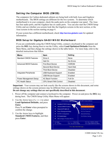
Transcription
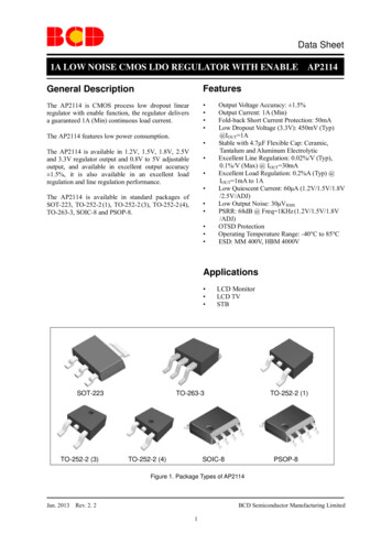
Data Sheet1A LOW NOISE CMOS LDO REGULATOR WITH ENABLEGeneral DescriptionFeaturesThe AP2114 is CMOS process low dropout linearregulator with enable function, the regulator deliversa guaranteed 1A (Min) continuous load current. The AP2114 features low power consumption. The AP2114 is available in 1.2V, 1.5V, 1.8V, 2.5Vand 3.3V regulator output and 0.8V to 5V adjustableoutput, and available in excellent output accuracy 1.5%, it is also available in an excellent loadregulation and line regulation performance. The AP2114 is available in standard packages ofSOT-223, TO-252-2 (1), TO-252-2 (3), TO-252-2 (4),TO-263-3, SOIC-8 and PSOP-8. AP2114Output Voltage Accuracy: 1.5%Output Current: 1A (Min)Fold-back Short Current Protection: 50mALow Dropout Voltage (3.3V): 450mV (Typ)@IOUT 1AStable with 4.7μF Flexible Cap: Ceramic,Tantalum and Aluminum ElectrolyticExcellent Line Regulation: 0.02%/V (Typ),0.1%/V (Max) @ IOUT 30mAExcellent Load Regulation: 0.2%A (Typ) @IOUT 1mA to 1ALow Quiescent Current: 60μA (1.2V/1.5V/1.8V/2.5V/ADJ)Low Output Noise: 30μVRMSPSRR: 68dB @ Freq 1KHz (1.2V/1.5V/1.8V/ADJ)OTSD ProtectionOperating Temperature Range: -40 C to 85 CESD: MM 400V, HBM 4000VApplications SOT-223TO-252-2 (3)LCD MonitorLCD TVSTBTO-263-3TO-252-2 (4)TO-252-2 (1)SOIC-8PSOP-8Figure 1. Package Types of AP2114Jan. 2013Rev. 2. 2BCD Semiconductor Manufacturing Limited1
Data Sheet1A LOW NOISE CMOS LDO REGULATOR WITH ENABLEAP2114Pin ConfigurationH/HA Package(SOT-223)HS Package(TO-263-3)HAD/DA PackageDDA(TO-252-2 (1))VOUT(TO-252-2 (3))(TO-252-2 (1))3VIN3VIN3VOUT2VOUT VOUT2VOUT GND2GND1GND1GND1VIN(TO-252-2 VIN418ENVIN18VOUTVOUT27GND GND27VIN6GND GND45GNDFor Fixed VersionsENVOUT2GND1VIN3VOUT2GND1VINMP Package(PSOP-8)GND3GND3(TO-252-2 (4))M Package(SOIC-8)GND(TO-252-2 (3))3465For Adjustable For Fixed VersionsFor Adjustable VersionFigure 2. Pin Configuration of AP2114 (Top View)Jan. 2013Rev. 2. 2BCD Semiconductor Manufacturing Limited2
Data Sheet1A LOW NOISE CMOS LDO REGULATOR WITH ENABLEAP2114Pin DescriptionsPin NumberSOT-223 (H),TO-263-3,TO-252-2 (1) (D)TO-252-2 (3) (D)TO-252-2 (4) (D)123SOT-223 (HA),TO-252-2 (1) (DA)TO-252-2 (3) (DA)TO-252-2 (4) 311, 3, 5, 6, 7242, 3, 5, 781GNDVOUTVIN84EN6ADJFunctionGroundRegulated OutputInput Voltage PinChip Enable, H–NormalWork, L– Shutdown OutputAdjust OutputFunctional Block DiagramEN(8)3 (4) {1}ShutdownLogicVINFoldbackCurrent LimitThermalShutdown2 (2) {3}VOUT3MΩVREFGND1 (1 , 3 , 5 , 6 , 7) {2}A (B) {C}A : SOT- 223 (H) , TO-263-3 , TO- 252- 2 (1)/(3)/(4)(D)B : SOIC-8 , PSOP-8C: SOT- 223 (HA) , TO- 252- 2 (1)/(3)/(4) (DA)For Fixed VersionsJan. 2013Rev. 2. 2BCD Semiconductor Manufacturing Limited3
Data Sheet1A LOW NOISE CMOS LDO REGULATOR WITH ENABLEAP2114Functional Block Diagram backCurrent Limit3 MΩ8VREFVOUT62, 3, 5, 7ADJGNDSOIC-8 , PSOP-8For ADJ VersionFigure 3. Functional Block Diagram of AP2114Jan. 2013Rev. 2. 2BCD Semiconductor Manufacturing Limited4
Data Sheet1A LOW NOISE CMOS LDO REGULATOR WITH ENABLEAP2114Ordering InformationAP2114PackageCircuit TypeG1: GreenPackageH/HA: SOT-223D/DA: TO-252-2 (1)/(3)/(4)S: TO-263-3M: SOIC-8MP: PSOP-8Blank: TubeTR: Tape & ReelTemperatureRangeSOT-223-40 to 85 CSOT-223-40 to 85 CTO-252-2 (1)/TO-252-2 (3)/TO-252-2 (4)-40 to 85 CTO-252-2 (1)/TO-252-2 (3)/TO-252-2 (4)-40 to 85 CTO-263-3-40 to 85 CSOIC-8-40 to 85 COutputVoltage1.2V (H)1.5V (H)1.8V (H)2.5V (H)3.3V (H)1.2V (HA)1.5V (HA)1.8V (HA)2.5V (HA)3.3V (HA)1.2V (D)1.5V (D)1.8V (D)2.5V (D)3.3V (D)1.2V (DA)1.5V (DA)1.8V (DA)2.5V (DA)3.3V . 2013-1.2: Fixed Output 1.2V1.5: Fixed Output 1.5V1.8: Fixed Output 1.8V2.5: Fixed Output 2.5V3.3: Fixed Output 3.3VADJ: ADJ OutputPart 1AP2114M-3.3TRG1AP2114M-ADJG1AP2114M-ADJTRG1Rev. 2. 2Marking M-2.5G12114M-3.3G12114M-ADJG12114M-ADJG1Tape & ReelTape & ReelTape & ReelTape & ReelTape & ReelTape & ReelTape & ReelTape & ReelTape & ReelTape & ReelTape & ReelTape & ReelTape & ReelTape & ReelTape & ReelTape & ReelTape & ReelTape & ReelTape & ReelTape & ReelTape & ReelTape & ReelTape & ReelTape & ReelTape & ReelTape & ReelTape & ReelTape & ReelTape & ReelTape & ReelTubeTape & ReelBCD Semiconductor Manufacturing Limited5
Data Sheet1A LOW NOISE CMOS LDO REGULATOR WITH ENABLEAP2114Ordering Information (Continued)PackageTemperatureRangePSOP-8-40 to 85 COutputVoltage1.2V1.5V1.8V2.5V3.3VADJPart AP2114MP-ADJTRG1Marking e & ReelTape & ReelTape & ReelTape & ReelTape & ReelTubeTape & ReelBCD Semiconductor's Pb-free products, as designated with "G1" suffix in the part number, are RoHS compliantand Green.Jan. 2013Rev. 2. 2BCD Semiconductor Manufacturing Limited6
Data Sheet1A LOW NOISE CMOS LDO REGULATOR WITH ENABLEAP2114Absolute Maximum Ratings (Note 1)ParameterSymbolValueUnitVIN6.5VPower Supply VoltageOperating Junction TemperatureRangeStorage Temperature RangeTJ150ºCTSTG-65 to 150ºCLead Temperature (Soldering, 10sec)TLEAD260ºCThermal Resistance (Junction toAmbient)(No Heatsink)θJASOIC-8144PSOP-8143SOT-223TO-252-2 (1)/TO-252-2 (3)/TO-252-2 (4)TO-263-3128 C/W9073ESD (Machine Model)400VESD (Human Body Model)4000VNote 1: Stresses greater than those listed under “Absolute Maximum Ratings” may cause permanent damage tothe device. These are stress ratings only, and functional operation of the device at these or any other conditionsbeyond those indicated under “Recommended Operating Conditions” is not implied. Exposure to “AbsoluteMaximum Ratings” for extended periods may affect device reliability.Recommended Operating ConditionsParameterSupply VoltageOperating AmbientRangeJan. 2013TemperatureSymbolMinMaxUnitVIN2.56.0VTA-4085 CRev. 2. 2BCD Semiconductor Manufacturing Limited7
Data Sheet1A LOW NOISE CMOS LDO REGULATOR WITH ENABLEAP2114Electrical CharacteristicsAP2114-1.2 Electrical Characteristics (Note 2)(VIN 2.5V, CIN 4.7μF (Ceramic), COUT 4.7μF (Ceramic), Typical TA 25 C, Bold typeface applies over -40OC TA 85OCranges, unless otherwise specified (Note 3))ParameterSymbolOutput VoltageVOUTInput VoltageTest ConditionsVIN 2.5V, 1mA IOUT 30mAIOUT(MAX)VIN 2.5V, VOUT 1.182V to 1.218VLoad Regulation VOUT/VOUT IOUTVIN 2.5V, 1mA IOUT 1ALine Regulation VOUT/VOUT VIN2.5V VIN 6V, IOUT 30mADropout VoltageVDROPQuiescent CurrentIQSupplyRejectionOutput VoltageTemperature CoefficientShort Current LimitMaxUnitVOUT 98.5%1.2VOUT 101.5%V6.0VPSRR VOUT/VOUT TISHORTIOUT 1.0AVIN 2.5V, IOUT 0mARipple 1Vp-pVIN 2.5V,IOUT 100mA1300mV6075μAVOUT 0V50mA30μVRMSStandby CurrentISTDVIN 2.5V, VEN in OFF modeThermal Resistance(Junction to Case)1200ppm/ CEnable logic low, regulator offShutdown%/V 30VILShutdown0.1IOUT 30mA, TA -40 C to 85 CVEN Low VoltageRDCHG0.02dBEnable logic high, regulator onVOUT Discharge Resistor%/A68VIHRPD1f 1KHzVEN High VoltagetS0.26810Hz f 100kHz (No Load)EN Pull Down ResistorAf 100HzVNOISEStart-up Time1-0.1RMS Output mum Output CurrentPowerRatioMinNo LoadSet EN pin at JC1.0V CSOIC-8PSOP-8SOT-223TO-252-2 (1) /(3) /(4)TO-263-374.643.750.93522 C/WNote 2: To prevent the Short Circuit Current protection feature from being prematurely activated, the inputvoltage must be applied before a current source load is applied.Note 3: Production testing at TA 25 C. Over temperature specifications guaranteed by design only.Jan. 2013Rev. 2. 2BCD Semiconductor Manufacturing Limited8
Data Sheet1A LOW NOISE CMOS LDO REGULATOR WITH ENABLEAP2114Electrical Characteristics (Continued)AP2114-1.5 Electrical Characteristics (Note 2)(VIN 2.5V, CIN 4.7μF (Ceramic), COUT 4.7μF (Ceramic), Typical TA 25 C, Bold typeface applies over -40OC TA 85OCranges, unless otherwise specified (Note 3))ParameterSymbolOutput VoltageVOUTInput VoltageTest ConditionsVIN 2.5V, 1mA IOUT 30mAIOUT(MAX)VIN 2.5V, VOUT 1.478V to 1.523VLoad Regulation VOUT/VOUT IOUTVIN 2.5V, 1mA IOUT 1ALine Regulation VOUT/VOUT VIN2.5V VIN 6V, IOUT 30mADropout VoltageVDROPQuiescent CurrentIQSupplyRejectionOutput VoltageTemperature CoefficientShort Current LimitMaxUnitVOUT 98.5%1.5VOUT 101.5%V6.0VPSRR VOUT/VOUT TISHORT%/A0.020.1%/VIOUT 1.0A8001000mVVIN 2.5V, IOUT 0mA6075μARipple 1Vp-pVIN 2.5V,IOUT 100mA-0.1f 100Hz68f 1KHz68dBIOUT 30mA, TA -40 C to 85 C 30ppm/ CVOUT 0V50mA30μVRMS10Hz f 100kHz (No Load)VEN High VoltageVIHEnable logic high, regulator onVEN Low VoltageVILEnable logic low, regulator offStandby CurrentISTDVIN 2.5V, VEN in OFF modetSEN Pull Down ResistorRPDVOUT Discharge ResistorRDCHGShutdownShutdownThermal Resistance(Junction to Case)A1VNOISEStart-up Time10.2RMS Output mum Output CurrentPowerRatioMinNo LoadSet EN pin at JC1.0V CSOIC-8PSOP-8SOT-223TO-252-2 (1) /(3) /(4)TO-263-374.643.750.93522 C/WNote 2: To prevent the Short Circuit Current protection feature from being prematurely activated, the inputvoltage must be applied before a current source load is applied.Note 3: Production testing at TA 25 C. Over temperature specifications guaranteed by design only.Jan. 2013Rev. 2. 2BCD Semiconductor Manufacturing Limited9
Data Sheet1A LOW NOISE CMOS LDO REGULATOR WITH ENABLEAP2114Electrical Characteristics (Continued)AP2114-1.8 Electrical Characteristics (Note 2)(VIN 2.8V, CIN 4.7μF (Ceramic), COUT 4.7μF (Ceramic), Typical TA 25 C, Bold typeface applies over -40OC TA 85OCranges, unless otherwise specified (Note 3))ParameterSymbolOutput VoltageVOUTMaximum Output Current VOUT/VOUT IOUT VOUT/VOUT VINLoad RegulationLine RegulationDropout VoltageVDROPQuiescent CurrentPowerRatioSupplyIOUT(MAX)IQRejectionOutput VoltageTemperature CoefficientPSRR VOUT/VOUT TTest ConditionsVIN 2.8V, 1mA IOUT 30mAVIN 2.8V, VOUT 1.773V to 1.827VMinTypMaxUnitVOUT 98.5%1.8VOUT 101.5%V1.0VIN 2.8V, 1mA IOUT 1AA0.21.0%/A0.020.1%/VIOUT 1.0A500700mVVIN 2.8V, IOUT 0mA6075μA2.8V VIN 6V, IOUT 30mARipple 1Vp-pVIN 2.8V,IOUT 100mA-0.1f 100Hz68f 1KHz68dBIOUT 30mA, TA -40 C to 85 C 30ppm/ CShort Current LimitISHORTVOUT 0V50mARMS Output NoiseVNOISE10Hz f 100kHz (No load)30μVRMSVEN High VoltageVIHEnable logic high, regulator onVEN Low VoltageVILEnable logic low, regulator offStandby CurrentISTDVIN 2.8V, VEN in OFF modeStart-up TimetSEN Pull Down ResistorRPDVOUT Discharge utdownShutdownThermal Resistance(Junction to Case)No LoadSet EN pin at JC1.0V CSOIC-874.6PSOP-843.7SOT-22350.9TO-252-2 (1) /(3) /(4)35TO-263-322 C /WNote 2: To prevent the Short Circuit Current protection feature from being prematurely activated, the inputvoltage must be applied before a current source load is applied.Note 3: Production testing at TA 25 C. Over temperature specifications guaranteed by design only.Jan. 2013Rev. 2. 2BCD Semiconductor Manufacturing Limited10
Data Sheet1A LOW NOISE CMOS LDO REGULATOR WITH ENABLEAP2114Electrical Characteristics (Continued)AP2114-2.5 Electrical Characteristics (Note 2)(VIN 3.5V, CIN 4.7μF (Ceramic), COUT 4.7μF (Ceramic), Typical TA 25 C, Bold typeface applies over -40OC TA 85OCranges, unless otherwise specified (Note 3))ParameterSymbolOutput VoltageVOUTMaximum Output CurrentIOUT(MAX)Test ConditionsVIN 3.5V, 1mA IOUT 30mAVIN 3.5V, VOUT 2.463V to 2.537VLoad Regulation VOUT/VOUT IOUTVout 2.5V, VIN Vout 1V1mA IOUT 1ALine Regulation VOUT/VOUT VIN3.5V VIN 6V, IOUT 30mADropout VoltageVDROPQuiescent CurrentIQPowerRatioSupplyRejectionOutput VoltageTemperature CoefficientPSRR VOUT/VOUT TMinTypMaxUnitVOUT 98.5%2.5VOUT 101.5%V1.0A0.21.0%/A0.020.1%/VIOUT 1A450750mVVIN 3.5V, IOUT 0mA6080μARipple 1Vp-pVIN 3.5V,IOUT 100mAf 100Hz65f 1KHz65-0.1dBIOUT 30mA 30ppm/ CShort Current LimitISHORTVOUT 0V50mARMS Output NoiseVNOISE10Hz f 100kHz30μVRMSVEN High VoltageVIHEnable logic high, regulator onVEN Low VoltageVILEnable logic low, regulator offStandby CurrentISTDVIN 3.5V, VEN in OFF modeStart-up TimetSEN Pull Down ResistorRPDVOUT Discharge utdownShutdownThermal Resistance(Junction to Case)No LoadSet EN pin at JC1.0V CSOIC-874.6PSOP-843.7SOT-22350.9TO-252-2 (1) /(3) /(4)35TO-263-322 C /WNote 2: To prevent the Short Circuit Current protection feature from being prematurely activated, the inputvoltage must be applied before a current source load is applied.Note 3: Production testing at TA 25 C. Over temperature specifications guaranteed by design only.Jan. 2013Rev. 2. 2BCD Semiconductor Manufacturing Limited11
Data Sheet1A LOW NOISE CMOS LDO REGULATOR WITH ENABLEAP2114Electrical Characteristics (Continued)AP2114-3.3 Electrical Characteristics (Note 2)(VIN 4.3V, CIN 4.7μF (Ceramic), COUT 4.7μF (Ceramic), Typical TA 25 C, Bold typeface applies over -40OC TA 85OCranges, unless otherwise specified (Note 3))P
1.8: Fixed Output 1.8V 2.5: Fixed Output 2.5V 3.3: Fixed Output 3.3V ADJ: ADJ Output Package H/HA: SOT-223 D/DA: TO-252-2 (1)/(3)/(4) S: TO-263-3 M: SOIC-8 MP: PSOP-8 . Data Sheet 1A LOW NOISE CMOS LDO REGULATOR WITH ENABLE AP2114 Jan. 2013 Rev. 2. 2 BCD Semiconductor Manufacturing Limited 6 Ordering Information (Continued) Package Temperature Range Output