Transcription
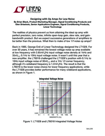
Designing with Op Amps for Low NoiseBy Brian Black, Product Marketing Manager, Signal Conditioning Products andGlen Brisebois, Senior Applications Engineer, Signal Conditioning Products,Linear TechnologyThe realities of physics prevent us from attaining the ideal op amp withperfect precision, zero noise, infinite open-loop gain, slew rate, and gainbandwidth product. But we expect successive generations of amplifiers tobe better than the previous. What then to make of low 1/f noise op amps?Back in 1985, George Erdi of Linear Technology designed the LT1028. Forover 30 years, it has remained the lowest voltage noise op amp availableat low frequency with 0.85nV/ Hz input voltage noise density at 1kHz and35nVP-P 0.1Hz to 10Hz input voltage noise. It wasn’t until this year that anew amplifier, the LT6018 challenged the LT1028’s position with 0.1Hz to10Hz input voltage noise of 30nVP-P and a 1Hz 1/f corner frequency,although it’s wideband frequency is 1.2nV/ Hz. The result is that theLT6018 is the lower noise choice for lower frequency applications, whilethe LT1028 provides better performance for many wideband applications,as shown in Figure 1.Figure 1: LT1028 and LT6018 Integrated Voltage NoiseS64, EN
A Noisy Noise AnnoysBut there is more to designing low noise circuits than choosing the lowestvoltage noise density (en) amplifier for a given frequency band. As shown inFigure 2, other noise sources come into play, with incoherent sourcescombining as a root sum of squares.in-in Req- R1 R2Req RSFigure 2: Op Amp Circuit Noise SourcesFirst, consider resistors as noise sources. Resistors inherently have noise,proportional to the square root of the resistance value. At a temperature of300K, the voltage noise density of any resistor is en 0.13 R nV/ Hz. Thisnoise can also be considered as a Norton equivalent current noise: in en/R 0.13/ R nA/ Hz. Resistors therefore have a noise power of 17zeptoWatts. Good op amps will have lower noise power than this. Forexample, the LT6018 noise power (measured at 1KHz) is about 1zeptoWatt.In the op amp circuit of Figure 2, the source resistance, gain resistor, andfeedback resistor (RS, R1, and R2 respectively) all contribute to the circuitnoise. When calculating noise, the “per root Hertz” used in voltage noisedensity can be confusing. But noise power is what adds together, not2
noise voltage. So to calculate the integrated voltage noise of a resistor orop amp, multiply the voltage noise density by the square root of thenumber of Hertz in the frequency band. For example, a 100Ω resistor has1.3μV RMS noise over a 1MHz bandwidth (0.13nV/ Ω * 100Ω * 1,000,000Hz). For a circuit with a first order rather than brick wall filter,the bandwidth would be multiplied by 1.57 to capture the noise in thehigher bandwidth skirt. To express the noise as peak-to-peak rather thanRMS, multiply by a factor of 6 (not 2.8, as you would for a sinusoid). Withthese considerations, the noise of this 100Ω resistor with a simple 1MHzlow-pass filter is closer to 9.8μVP-P.Also, the op amp has input current noise associated with the current intoor out of each input, in- and in . These multiply by the resistances they workinto, R1 in parallel with R2 in the case of in- and RS in the case of in tocreate voltage noise through the magic of Ohm’s law. Looking inside theamplifier (Figure 3), this current noise is comprised of multiple sources.Figure 3: Coherent and Incoherent Noise Sources in an Op Amp Diff PairConsidering the wideband noise, each of the two input transistors haveshot noise associated with their base, ini- and ini , which are not coherent.The noise from the current source in the input pair tail, int also createscoherent noise split between the two inputs (int/2β in each). If theresistance seen by the two inputs is equal, the coherent voltage noise ateach input is also equal and cancels according to the amplifier’s commonmode rejection capability, leaving primarily the incoherent noise. This islisted as the balanced current noise in data sheets. If the resistance seen3
at the two inputs is greatly mismatched, then the coherent and incoherentnoise components remain and the voltage noise adds as the root sum ofsquares. This is listed in some data sheets as unbalanced noise current.Both the LT1028 and LT6018 have lower voltage noise than a 100Ωresistor (which at room temperature is 1.3nV/ Hz), so where sourceresistances are higher, the op amp’s voltage noise will often not be thelimiting factor for noise in the circuit. In cases where the sourceresistances are much lower, the amplifier’s voltage noise will begin todominate. For very high source resistances, the amplifier’s current noisedominates, and in the middle the Johnson noise of the resistors dominates(for well designed op amps which do not have excessively high noisepower). The resistance at which the amplifier current noise and voltagenoise are balanced so that neither dominates is equal to the amplifier’svoltage noise divided by its current noise. Since voltage and current noisevary with frequency so too does this midpoint resistance. For anunbalanced source, at 10Hz the midpoint of LT6018 is approximately 86Ω;at 10kHz it is about 320Ω.Minimizing Circuit NoiseSo what is the design engineer to do to minimize noise? For processingvoltage signals, reducing the equivalent resistance below the amplifier’smidpoint resistance is a good place to start. For many applications thesource resistance is fixed by the preceding stage, often a sensor. The gainand feedback resistors can be chosen to be small. However since thefeedback resistor forms part of the op amp load, there are limits due to theamplifier’s output drive capability and the acceptable amount of heat andpower dissipation. In addition to the resistance seen by the inputs, thefrequency should also be considered. The total noise consists of the noisedensity integrated over the entire frequency. Filtering noise at frequencieshigher (and perhaps also lower) than the signal bandwidth is important.In transimpedance applications, where the input to the amplifier is acurrent, a different strategy is needed. In this case, the Johnson noise ofthe feedback resistor increases as a square root factor of its resistancevalue, but at the same time the signal gain increase is linear with theresistance value. Hence the best SNR is achieved with as large aresistance as the voltage capability or the current noise of the op amp4
allows. For an interesting example, see the back page application on page26 of the LTC6090 data sheet.Noise and Other HeadachesNoise is just one source of error, and should be considered within thecontext of other error sources. Input offset voltage (the voltage mismatchat the op amp inputs) can be thought of as DC noise. Its impact can bereduced significantly by doing a one-time system calibration, but thisoffset voltage changes with temperature and time as a result of changes inmechanical stress. It also changes with input level (CMRR) and powersupply (PSRR). Real-time system calibration to cancel drift caused bythese variables quickly becomes expensive and impractical. For harshenvironment applications where the temperature fluctuates considerably,measurement uncertainty due to offset voltage and drift can dominate overnoise. For example, an op amp with 5μV/ C temperature drift canexperience an input-referred shift of 625μV from -40 C to 85 C due totemperature drift alone. Compared with this, a few hundred nanovolts ofnoise is inconsequential. The LT6018 has outstanding drift performance of0.5μV/ C and a maximum offset spec of 80μV from -40 C to 85 C. Foreven better performance, the recently released LTC2057 auto-zeroamplifier has a maximum offset voltage of less than 7μV from -40 C to125 C. Its wideband noise of 11nV/ Hz, and its DC to 10Hz noise is200nVP-P. While this is higher noise than the LT6018, the LTC2057 cansometimes be the better choice for low frequency applications due to itsoutstanding input offset drift over temperature. It is also worth noting thatdue to its low input bias current, the LT2057 has much lower current noisethan the LT6018. Another benefit of the LTC2057 low input bias current isthat it has very low clock feedthrough compared with many other zero-driftamplifiers. Some of these other zero-drift amplifiers can exhibit largevoltage noise spurs when source impedance is high.In such high precision circuits, care must also be taken to minimizethermocouple effects, which occur anywhere that there is a junction ofdissimilar metals. Even junctions of two copper wires from differentmanufacturers can generate thermal EMFs of 200nV/ C, over 13 times theworst-case drift of the LTC2057. Layout techniques to match or minimizethe number of junctions in the amplifier’s input signal path, keep inputsand matching junctions close together, and avoiding thermal gradients areimportant in these low drift circuits.5
ConclusionNoise is a fundamental physical limitation. To minimize its effects inprocessing sensor signals, care must be taken in choosing a suitable opamp, in minimizing and matching input resistances, and in the physicallayout of the design.6
zeptoWatts. Good op amps will have lower noise power than this. For example, the LT6018 noise power (measured at 1KHz) is about 1 zeptoWatt. In the op amp circuit of Figure 2, the source resistance, gain resistor, and feedback resistor (R S, R 1, a