Transcription
AN3105Application note48 V - 130 W high efficiency converter with PFC for LED streetlighting applications - European versionBy Claudio SpiniIntroductionNowadays, LEDs are becoming ever more popular, thanks to their particular characteristics,such as high efficiency and long life, and therefore they are pushing the innovation of currentlamp types and strongly contributing to reducing the energy consumption for internal orexternal lighting. This is also the case in street lighting applications, where higher efficiencyand long life are vital for reducing costs.For these reasons a street lighting power supply designed to power an LED lamp must havehigh efficiency and at least a similar lifetime, in order to guarantee the maintenance freeoperation required by these kinds of applications.This application note describes the characteristics and features of a 130 W demonstrationboard (EVL130W-SL-EU), tailored on an LED power supply specification for street lighting.The circuit is composed of two stages; a front-end PFC using the L6562AT and an LLCresonant converter based on the L6599AT.The peculiarities of this design are; very high efficiency, extended European input mainsrange (177-277 VAC) operation, and long term reliability.Because reliability (MTBF - “Mean Time Between Failures”) in power supplies is typicallyaffected by electrolytic capacitors and their typical high failure rate, unless using veryexpensive types, this board offers a very innovative design approach as the board doesn'timplement any electrolytic capacitors, which are replaced by film capacitors from EPCOS.Component de-rating has also been carefully applied during the design phase, decreasingthe component stress as recommended by MIL-HDBK-217D. The number of components,thanks to the use of the new L6562AT and L6599AT devices, has also been minimized,therefore increasing the MTBF and optimizing the total component cost. Thanks to the highefficiency achieved no heatsinks are required. The resonant stage power components areSMT, like most of the passive components, therefore decreasing production costs.The board also has protections in case of overload or short-circuit, open-loop by each stage,or input overvoltage. Because of the particular application, all protections, in the case ofintervention, are auto-restart.Figure 1.September 2012EVL130W-SL-EU: 130 W SMPS for LED street lighting applicationsDoc ID 16774 Rev 21/30www.st.comDownloaded from Arrow.com.
ContentsAN3105Contents1Main characteristics and circuit description . . . . . . . . . . . . . . . . . . . . . 41.1Power Factor corrector . . . . . . . . . . . . . . . . . . . . . . . . . . . . . . . . . . . . . . . . 41.2Resonant power stage . . . . . . . . . . . . . . . . . . . . . . . . . . . . . . . . . . . . . . . . 51.3Startup sequence . . . . . . . . . . . . . . . . . . . . . . . . . . . . . . . . . . . . . . . . . . . . 51.4Output voltage feedback loop . . . . . . . . . . . . . . . . . . . . . . . . . . . . . . . . . . . 51.5L6599AT overload and short-circuit protection . . . . . . . . . . . . . . . . . . . . . . 61.6Overvoltage and open-loop protection . . . . . . . . . . . . . . . . . . . . . . . . . . . . 62Efficiency measurement . . . . . . . . . . . . . . . . . . . . . . . . . . . . . . . . . . . . . . 83Input current harmonics measurement . . . . . . . . . . . . . . . . . . . . . . . . . . 94Functional check . . . . . . . . . . . . . . . . . . . . . . . . . . . . . . . . . . . . . . . . . . . 114.1PFC circuit . . . . . . . . . . . . . . . . . . . . . . . . . . . . . . . . . . . . . . . . . . . . . . . . 114.2Half-bridge resonant LLC circuit . . . . . . . . . . . . . . . . . . . . . . . . . . . . . . . . 114.3Dynamic load operation . . . . . . . . . . . . . . . . . . . . . . . . . . . . . . . . . . . . . . 134.4Overcurrent and overvoltage protection . . . . . . . . . . . . . . . . . . . . . . . . . . 144.5Converter startup . . . . . . . . . . . . . . . . . . . . . . . . . . . . . . . . . . . . . . . . . . . 164.6Thermal map . . . . . . . . . . . . . . . . . . . . . . . . . . . . . . . . . . . . . . . . . . . . . . 175Conducted emission pre-compliance test: peak measurement . . . . . 196Bill of material . . . . . . . . . . . . . . . . . . . . . . . . . . . . . . . . . . . . . . . . . . . . . 207PFC coil specifications . . . . . . . . . . . . . . . . . . . . . . . . . . . . . . . . . . . . . . 258Transformer specification . . . . . . . . . . . . . . . . . . . . . . . . . . . . . . . . . . . 279Revision history . . . . . . . . . . . . . . . . . . . . . . . . . . . . . . . . . . . . . . . . . . . 292/30Downloaded from Arrow.com.Doc ID 16774 Rev 2
AN3105List of figuresList of figuresFigure 1.Figure 2.Figure 3.Figure 4.Figure 5.Figure 6.Figure 7.Figure 8.Figure 9.Figure 10.Figure 11.Figure 12.Figure 13.Figure 14.Figure 15.Figure 16.Figure 17.Figure 18.Figure 19.Figure 20.EVL130W-SL-EU: 130 W SMPS for LED street lighting applications. . . . . . . . . . . . . . . . . . 1EVL130W-SL-EU demonstration board: electrical diagram . . . . . . . . . . . . . . . . . . . . . . . . . 7EVL130W-SL-EU demonstration board efficiency diagrams . . . . . . . . . . . . . . . . . . . . . . . . 8EVL130W-SL-EU demonstration board: compliance to EN61000-3-2 Class-C standard . . 9EVL130W-SL-EU demonstration board: input current waveform at 230 V - 50 Hz - 130 Wload and 65 W load. . . . . . . . . . . . . . . . . . . . . . . . . . . . . . . . . . . . . . . . . . . . . . . . . . . . . . . 10EVL130W-SL-EU demonstration board: Power Factor and Total Harmonic Distortion vs.load . . . . . . . . . . . . . . . . . . . . . . . . . . . . . . . . . . . . . . . . . . . . . . . . . . . . . . . . . . . . . . . . . . . 10EVL130W-SL-EU demonstration board: PFC stage and L6562AT waveforms at 230 V 50 Hz - full load – detail . . . . . . . . . . . . . . . . . . . . . . . . . . . . . . . . . . . . . . . . . . . . . . . . . . . 11EVL130W-SL-EU demonstration board: primary and secondary side resonant stagewaveforms at 230 V - 50 Hz - full load . . . . . . . . . . . . . . . . . . . . . . . . . . . . . . . . . . . . . . . . 12EVL130W-SL-EU demonstration board: high and low frequency ripple on output voltage at230 V - 50 Hz - full load . . . . . . . . . . . . . . . . . . . . . . . . . . . . . . . . . . . . . . . . . . . . . . . . . . . 13EVL130W-SL-EU demonstration board: output voltage variation driving a CC LED converter- PWM 90% and PWM 15% . . . . . . . . . . . . . . . . . . . . . . . . . . . . . . . . . . . . . . . . . . . . . 14EVL130W-SL-EU demonstration board: short-circuit at 230 VAC - 50 Hz - full load and openloop protection intervention at 20 W load . . . . . . . . . . . . . . . . . . . . . . . . . . . . . . . . . . . . . . 15EVL130W-SL-EU demonstration board: startup at 230 VAC - 50 Hz - full load . . . . . . . . . 16Thermal map at 230 VAC - 50 Hz - full load - PCB top side . . . . . . . . . . . . . . . . . . . . . . . . 17Thermal map at 230 VAC - 50 Hz - full load - PCB bottom side . . . . . . . . . . . . . . . . . . . . . 18CE peak measure at 230 VAC and full load - phase wire . . . . . . . . . . . . . . . . . . . . . . . . . . 19CE peak measure at 230 VAC and full load - neutral wire . . . . . . . . . . . . . . . . . . . . . . . . . 19PFC coil electrical diagram . . . . . . . . . . . . . . . . . . . . . . . . . . . . . . . . . . . . . . . . . . . . . . . . . 25PFC coil mechanical aspect(1) . . . . . . . . . . . . . . . . . . . . . . . . . . . . . . . . . . . . . . . . . . . . . . 26Transformer electrical diagram . . . . . . . . . . . . . . . . . . . . . . . . . . . . . . . . . . . . . . . . . . . . . . 27Transformer overall drawing . . . . . . . . . . . . . . . . . . . . . . . . . . . . . . . . . . . . . . . . . . . . . . . . 28Doc ID 16774 Rev 2Downloaded from Arrow.com.3/30
Main characteristics and circuit description1AN3105Main characteristics and circuit descriptionThe main features of the SMPS are:1.1 Extended European input mains range: 177 to 277 VAC - frequency 45 to 55 Hz Output voltage: 48 V at 2.7 A Long-life electrolytic capacitors are not used Mains harmonics: acc. to EN61000-3-2 Class-C Efficiency at full load: better than 90% EMI: according to EN55022-Class-B Safety: double insulation, according to EN60950, SELV Dimensions: 75 x 135 mm, 30 mm components maximum height No heatsinks needed PCB: single side, 35 µm, FR-4, mixed PTH/SMTPower Factor correctorThe PFC stage, working in transition mode, acts as a pre-regulator and powers the resonantstage with the output voltage of 450 V. The PFC power topology is a conventional boostconverter, connected to the output of the rectifier bridge D3. It is completed by the coil L1,manufactured by MAGNETICA, the diode D2 and the capacitors C5, C6, and C7 in parallel.The PFC output capacitors are film type, 5 µF - 800 V, manufactured by EPCOS. Using filmcapacitors to replace the typical electrolytic capacitors considerably increases the MTBF ofthe board.The boost switch is represented by the Power MOSFET Q2. The board is equipped with aninput EMI filter necessary to filter the commutation noise coming from the boost stage. ThePFC implements the L6562AT controller, a small and inexpensive controller which isguaranteed for operation over a wide temperature range.At startup, the L6562AT is supplied by the startup resistors R5, R8, and R13 charging thecapacitor C13; once the PFC begins switching, a charge pump connected to the auxiliarywinding of the PFC inductor L1 supplies both PFC and resonant controllers via a smalllinear regulator realized by Q1. Once both stages have been activated, the controllers arealso supplied by the auxiliary winding of the resonant transformer, assuring correct supplyvoltage during all load condition operations. The L1 auxiliary winding is also connected tothe L6562AT pin #5 (ZCD) through the resistor R18. Its purpose is to provide the informationthat L1 has demagnetized, needed by the internal logic to trigger a new switching cycle. ThePFC boost peak current is sensed by resistor R34 in series to the MOSFET source; thesignal is fed into pin #4 (CS) of the L6562AT, via the filter R27 and C16.The dividers R7, R12, R14, and R22 provide the information on the instantaneous mainsvoltage to the L6562AT multiplier which is used to modulate the peak current of the boost.The resistors R2, R6, R9 with R15 and R16 are dedicated to sensing the output voltage andfeed, to the L6562AT, the feedback information necessary to keep the output voltageregulated. The components C11 and R20 (C12 is shorted) make up the error amplifiercompensation network necessary to keep the required loop stability.4/30Downloaded from Arrow.com.Doc ID 16774 Rev 2
AN31051.2Main characteristics and circuit descriptionResonant power stageThe down-stream converter is a resonant LLC half-bridge stage working with 50 percentfixed duty cycle and variable frequency. It implements the ST L6599AT, integrating allfunctions necessary to properly control the resonant topology.The resonant transformer, manufactured by MAGNETICA, uses the integrated magneticapproach, so the leakage inductance is used for resonant operation of the circuit. Therefore,no external, additional coil is needed for the resonance. The transformer secondary windingconfiguration is the typical centre tap, using a couple of type STPS10150CG power Schottkyrectifiers. The output capacitors are film type, 4.7 µF - 63 V from EPCOS. Like for the PFCstage, using film capacitors allows to increase considerably the MTBF of the board.A small LC filter has been added on the output, in order to filter the high frequency ripple.D21, D22, and R55 implement a voltage controlled bleeder; in the case of no-load operationof the SMPS, this circuit provides a bleeder limiting the increase of output voltage, but notaffecting efficiency during normal operation. Please note that the converter has not beendesigned to work in this condition and therefore its mains consumption is not optimized( 3 W).1.3Startup sequenceThe PFC acts as master and therefore starts first; the resonant stage operates only if thePFC is delivering the nominal output voltage to prevent the resonant converter from workingwith a too low input voltage which can cause incorrect capacitive mode operation. Thereforeboth stages are designed to work according to this sequence.For correct sequencing, the L6599AT makes use of the LINE pin (#7) to sense the PFCoutput voltage via a resistor divider. The L6599AT LINE pin (#7) has an internal comparatorwhich has a hysteresis allowing the turn-on and turn-off voltage to be set independently. Atstartup, the LLC stage starts once the PFC output voltage reaches 430 V, while the turnoff threshold has been set to 330 V.1.4Output voltage feedback loopThe output voltage is kept stable by means of a feedback loop implementing a typical circuitusing a TS2431 to modulate the current in the optocoupler diode.On the primary side, R43 - connecting pin RFMIN (#4) to the optocoupler's phototransistor allows the L6599AT oscillator frequency to be modulated, therefore keeping the outputvoltage regulated. It also sets the maximum switching frequency at about 130 kHz. R42,which connects the same pin to ground, sets the minimum switching frequency. The R-Cseries R37 and C24 sets both soft-start maximum frequency and duration.All demonstration boards implement the voltage loop circuitry described above but in casea current loop is also required it can be achieved by implementing the following modifications: Replace R30 and R31 0R0 Ω resistors with sensing resistors, 0R033 and 0R039respectively, both 0805 Populate on PCB U4 and the relevant components reported on the schematic as N.M.:C36 1N0-0805; C37 100NF-0805; R51 15R-0805; R56 1K0-0805; R61 22K1206; C41 2N2-0805; U5 SEA05TR Remove the TS2431AILTDoc ID 16774 Rev 2Downloaded from Arrow.com.5/30
Main characteristics and circuit descriptionAN3105With these modifications the circuit is able to keep the output current constant at 2.7 A downto an output voltage value of around 30 V. This function can be used to optimize the voltagedrop and power dissipation in case current linear regulators are used to regulate the currentflowing in each LED strip. In case the output current is lower than the current loop setpoint,the voltage loop takes over the operation regulating the output voltage at its nominal value,like using the TS2431AILT.1.5L6599AT overload and short-circuit protectionThe current flowing into the primary winding, proportional to the output load, is sensed bythe lossless circuit C34, R53, D19, D18, R57, and C35 and it is fed into the ISEN pin (#6) ofL6599AT. In the case of overcurrent, the voltage on the pin overpasses an internal threshold(0.8 V), triggering a protection sequence. The capacitor (C21) connected to the DELAY pin(#2) is charged by an internal 150 µA current generator. If the voltage on the pin reaches2 V, the soft-start capacitor is completely discharged so that the switching frequency ispushed to its maximum value. As the voltage on the pin exceeds 3.5 V the IC stopsswitching and the internal generator is turned off, so that the voltage on the DELAY pindecays because of the external resistor connected between the pin and GND. The L6599ATis soft-restarted as the voltage drops below 0.3 V. In this way, under short-circuit conditions,the converter works intermittently with low input average power, limiting the stress ofcomponents during shorts.1.6Overvoltage and open-loop protectionBoth circuit stages, PFC and resonant, are equipped with their own overvoltage protections.The L6562AT PFC controller implements an overvoltage protection against the outputvoltage variation due to the poor bandwidth of the error amplifier, happening in the case oftransients. Unfortunately it cannot protect the circuit in the case of a feedback loop failuresuch as disconnection or deviation from the nominal value of the feedback loop divider. Inthe case where a similar failure condition is detected, the L6599AT pin DIS (#8) stops theoperation and also stops the PFC operation by means of the L6599AT pin PFC STOP (#9)connected to the L6562AT pin INV (#1). The converter operation is latched until the VCCcapacitors are discharged, then a new startup sequence takes place automatically and theconverter resumes operation if the failure is removed or a new sequence is triggered. Thesame sequence occurs also in the case of input voltage transients which may damage theconverter.The DIS pin is also used to protect the resonant stage against loop failures. The Zenerdiode D17 detects the auxiliary voltage generated by the LLC transformer. In the case ofloop failure, it conducts, and voltage on the DIS pin exceeds the internal threshold, latchingoff the device. The L6562AT operation is also stopped by the PFC STOP pin as in theprevious case, and after some time has elapsed the circuit restarts.6/30Downloaded from Arrow.com.Doc ID 16774 Rev 2
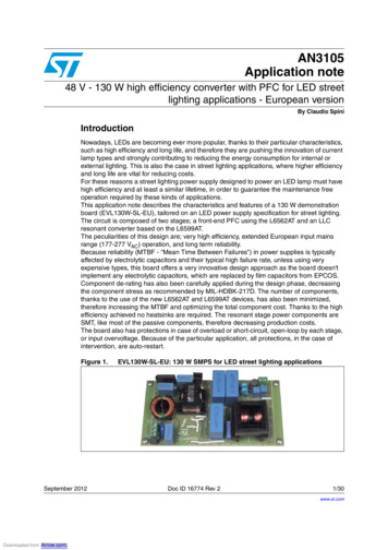
FUSE T4AF1R47VCCRX2R22Doc ID 16774 Rev 211C1515 nF23Z112N. M.R49R42C24N. M.R44567R37VCCZCDGNDGD8C13220 nFC32R43C910 nF911R5212218765R33N. 7R113L6599ATU2D9LL4148C25 3470 pF D5LL4148R3D17BZV55-B2410 nFC33C264.7 nFLL4148R36C21220 nFR27R38R13R8R5C4470 nF-X2VCCC31220 nFR1MULTCSU1R16L6562ATCOMPINVQ33N. M.VIN C16220 pF4321R15D10Q7BC847CD3GBU8JC3470 nF-X2N. M.R20C11220 nFC124PCB rev. 0.232L22019.00021C2470 nF-X2Q82 BC847C3R45R14R12R7177-277 VAC1RV1300 VACMKDS 1,5/ 3-5,08R34910111213 VCC1415C22100 nF163C30Q22 STF22NM60ND6LL4148D2STTH3L06UD24LL4148220 nFR26VINR39R57R4611C5C6C40D19LL4148RX1R533 Q4STD10NM60N23 48C35R25R9R6R2R4C34R59220 pFD20STPS1L60AGB6C715 nFC20131214108911REV. 0.9U334R622121C18C39470 nFN. M.R54R60R58R413U5TS2431AILTC38R50D22D21C41R611N. M.3N. M. 2R56N. M.R51N. M.VctrlIctrlOUT45I.sense VCC 6GND12N.M.C36C37N. M.48 V at 2.7 A100 nFC19J2MKDS 1,5/ 2-5,08U4SEA05 - N. M.R31R30L3R55R29N. M.BZV55-B24 TPS10150CGC27220 nFSFH617A-2X0097642T11860.0013C82.2 nF - Y1C12.2 nF - Y1Figure 2.23 Downloaded from Arrow.com. J1AN3105Main characteristics and circuit descriptionEVL130W-SL-EU demonstration board: electrical diagramAM008687/30
Efficiency measurement2AN3105Efficiency measurementTable 1 shows the overall efficiency, measured at 230 VAC - 50 Hz with different loads.At 230 VAC and full load the overall efficiency is 93.85%, making this design suitable for highefficiency power supplies. The efficiency has been measured at 25%, 50%, 75%, and 100%,the average efficiency calculated according to the ES-2 standard is 91.56%.Table 1.EVL130W-SL-EU demonstration board: overall efficiency vs. load230 V-50 HzLoadVOUT [V]IOUT [A]POUT [W]PIN [W]Efficiency [%]25% load47.590.68232.4637.1487.39%50% load47.551.3765.1470.8991.89%75% load47.542.0095.08102.193.12%100% load47.542.74130.26138.893.85%Average efficiency91.56%The measured output voltage at different load conditions is reported in Table 1. As seen, thevoltage is very stable over all the output load range.The measured efficiency is shown on the lefthand side of the graph in Figure 3, while on therighthand side of Figure 3 the efficiency, at maximum load and at minimum, nominal, andmaximum AC input voltage, is reported.Figure 3.EVL130W-SL-EU demonstration board efficiency diagrams%FFICIENCY VS 6!# %FFICIENCY%FFICIENCY%FFICIENCY VS LOAD ,OAD8/30Downloaded from Arrow.com. 6!# ;6RMS Doc ID 16774 Rev 2 !-
AN3105Input current harmonics measurement3Input current harmonics measurementOne of the main purposes of a PFC pre-conditioner is the correction of input currentdistortion, decreasing the harmonic contents below the limits of the relevant regulations.Therefore, this demonstration board has been tested according to the European standardEN61000-3-2 Class-C relevant to lighting equipment, at full load and nominal input voltagemains. Measurement results are in Figure 4 - on the lefthand side.The circuit shows its ability to reduce the harmonics, also well below the limits ofEN61000-3-2 Class-C regulation, not only at full load but also at significant lower load; onthe righthand side of Figure 4 the input current harmonics measurement at light load(minimum input power to be compliant with the above mentioned rule is 25 W) shows thateven if the power supply is working out of its typical operating region it is still compliant withthe EN61000-3-2 Class-C limits.Figure 4.EVL130W-SL-EU demonstration board: compliance to EN61000-3-2 Class-C standard (ARMONIC CURRENT ;! (ARMONIC CURRENT ;! (ARMONIC ORDER ;N (ARMONIC ORDER ;N -EASURED VALUE%. #LASS # LIMITS!- VIN 230 VAC - 50 Hz, POUT 130 WTHD 6.85%, PF 0.981VIN 230 VAC - 50 Hz, PIN 26.7 WTHD 10.3%, PF 0.753Doc ID 16774 Rev 2Downloaded from Arrow.com.9/30
Input current harmonics measurementAN3105For user reference, waveforms of the input current and voltage at nominal input voltagemains full load and 50% load conditions are given in Figure 5.Figure 5.EVL130W-SL-EU demonstration board: input current waveform at 230 V - 50 Hz- 130 W load and 65 W loadCH1: VIN ACCH1: VIN ACCH4: I ACCH4: I ACThe “Power Factor” (PF) and the “Total Harmonic Distortion” (THD) versus load variationshave also been measured and the results are given in Figure 6. As seen, the Power Factorremains close to unity and the Total Harmonic Distortion is very low.Figure 6.EVL130W-SL-EU demonstration board: Power Factor and Total Harmonic Distortionvs. load4( VS LOAD 4( 0OWER &ACTOR0OWER &ACTOR VS LOAD ,OAD,OAD!- 10/30Downloaded from Arrow.com.Doc ID 16774 Rev 2
AN3105Functional check4Functional check4.1PFC circuitOn the lefthand side of Figure 7, some waveforms relevant to the PFC stage have beencaptured; the envelope of CS pin (#4) waveforms of the L6562AT is in phase with the MULTpin (3#) and has the same sinusoidal shape, demonstrating the correct functioning of thePFC stage. It is also possible to measure the peak-to-peak value of voltage ripple overimposed to the PFC output voltage; this is due to the low value of the PFC output capacitors.On the righthand side of Figure 7 the details of some waveforms at switching frequency aregiven.Figure 7.EVL130W-SL-EU demonstration board: PFC stage and L6562AT waveforms at 230 V 50 Hz - full load – detailCH2: VOUT PFCCH4: MULT4.2CH3: CSCH3: CSCH1: Vdrain Q2CH4: ZCDCH2: VOUT PFCHalf-bridge resonant LLC circuitSome waveforms relevant to the resonant stage during steady-state operation are given inthe following pages. The resonant stage switching frequency is about 100 kHz, in order tohave a good trade off between transformer losses and dimensions.The LLC converter has been designed to operate at nominal voltage and full load at theresonance frequency, but due to the PFC output voltage ripple at twice the mains frequencyit is driven slightly above and below the resonant tank frequency, according to theinstantaneous value of PFC output voltage.In Figure 8 (on the lefthand side) some waveforms relevant to the resonant stage ZVSoperation are shown; it is possible to see that both MOSFETs are turned on when resonantcurrent is flowing through their body diodes and therefore drain-source voltage is almostzero, achieving good efficiency because the turn-on losses are negligible. The HB MOSFETvoltage de-rating and low operating temperature allow the board MTBF to be increased.The current flowing in the resonant tank is sinusoidal; in Figure 8 it is possible to appreciatea slight asymmetry of operating modes by each half portion of the sinewave; half cycle isworking at resonant frequency while the other is working above the resonant frequency. ThisDoc ID 16774 Rev 2Downloaded from Arrow.com.11/30
Functional checkAN3105is due to a small difference between each half-secondary leakage inductance of thetransformer reflected to the primary side, providing the two slightly different resonantfrequencies. This phenomenon is typically due to a different coupling of transformersecondary windings and in this case it is not an issue. The slight asymmetry can also beappreciated in Figure 8 (on the righthand side); the small ringing appearing on bothsecondary rectifiers anode voltage indicates that for a short time the rectifiers are notconducting; it demonstrates that during half cycle the circuit is working below the resonantfrequency while during the following half cycle it is working at resonance frequency.In Figure 8 it is also possible to appreciate the rectifier operating voltage and its margin withrespect to the maximum reverse voltage (VRRM). This de-rating with respect to the rectifiersVRRM guarantees good reliability of the output rectifiers increasing the board total MTBF.Figure 8.EVL130W-SL-EU demonstration board: primary and secondary side resonant stagewaveforms at 230 V - 50 Hz - full loadCH1: HB voltageCH3: VCC12/30Downloaded from Arrow.com.CH2: CF pin voltageCH4: res. tank currentCH1: V D12CH3: VOUTDoc ID 16774 Rev 2CH2: V D11
AN3105Functional checkOn the lefthand side of Figure 9 the high frequency ripple has been measured; as seen theripple and noise at switching frequency is very limited, thanks to the low EMI generated byboth stages. On the righthand side of Figure 9 the low frequency ripple has also beenmeasured. It is possible to note that the peak-to-peak value is not so low but it doesn't affectthe application, in fact the converters regulating the current flowing in each LED strip canreject the ripple without any problem.Figure 9.CH3: VOUT4.3EVL130W-SL-EU demonstration board: high and low frequency ripple on outputvoltage at 230 V - 50 Hz - full loadCH1: HB voltageCH3: VOUTDynamic load operationWaveforms reported in Figure 10 are relevant to the demonstration board during operation,supplying converters dedicated to power LED strips with constant current.In both figures it is possible to see the output voltage modulation during operation withvariable load due to the dimming of the LED current by PWM. For both measurements,a dimming frequency of 300 Hz has been chosen.On the lefthand side of Figure 10 the converter output current was 2.6 A and dimming dutycycle was 90%, therefore very close to the converter nominal output power. The outputvoltage in the image has two modulations; one is due to the rejection of the PFC outputvoltage ripple already measured in Figure 9, on the righthand side. Over imposed there isthe voltage variation due to the LED current dimming. The peak-to-peak variation is 5.37 V,this doesn't create any problems for the load as the converters reject the modulation.Whereas on the righthand side of Figure 10 the converter has been checked at light load, sothe peak output current was 3 A and dimming duty cycle was 15%, for an output power of21 W. Even in this case the peak-to-peak modulation doesn't give any trouble to the downstream current regulators and the board still works correctly.Doc ID 16774 Rev 2Downloaded from Arrow.com.13/30
Functional checkAN3105Figure 10. EVL130W-SL-EU demonstration board: output voltage variation drivinga CC LED converter - PWM 90% and PWM 15%CH1: PWM dimming signalCH4: SMPS output currentCH2: VOUTCH1: PWM dimming signalCH4: SMPS output currentCH2: VOUTIt is worth clarifying that, for correct operation with LED strips, the board needs someadditional capacitors connected on the 48 V output bus. It has not been equipped with allthe capacitors necessary for correct operation with LEDs but only with minimumcapacitance to allow board operation, in order to optimize the system cost and reliability.The additional capacitors needed are intended to be placed close to each LED strip currentregulator, therefore filtering the EMI generated by these. In several cases, in fact, the powersupply is placed at the base of the lighting pole while the LED current regulators are locatedon top, in the lamp. The long wiring connection between the power supply and theconverters can act as an antenna radiating EMI. Therefore local filtering minimizes theradiated EMI.The capacitance to be added to the 48 V bus, for correct operation with LEDs, is around40 µF. In order to not affect the board MTBF, using the same capacitor type already used onthe power supply board is suggested.4.4Overcurrent and overvoltage protectionThe L6599AT is equipped with a current sensing input (pin #6, ISEN) and a dedicatedovercurrent management system. The current flowing in the resonant tank is detected andthe signal is fed into the ISEN pin. It is internally connected to a first comparator, referencedto 0.8 V, and to a second comparator referenced to 1.5 V. If the voltage externally applied tothe pin exceeds 0.8 V, the first comparator is tripped causing an internal switch to be turnedon and discharging the soft-start capacitor C24 (CSS). Under output short-circuit, thisoperation results in a nearly constant peak primary current.With the L6599AT the designer can program externally the maximum time that the converteris allowed to run overloaded or under short-circuit conditions. Overloads or short-circuitslasting less than the set time do not cause any other action, and so provide the system withimmunity to short duration phenomena. If, instead, an overload condition continues,a protection procedure is activated which shuts down the L6599AT. In the case ofcontinuous overload or short-circuit, it results in continuous intermittent operation witha user defined duty cycle.14/30Downloa
All demonstration boards implement the voltage loop circuitry described above but in case a current loop is also required it can be achieved by implementing the following modifications: Replace R30 and