Transcription
Altera Quartus II TutorialECE 552Quartus II by Altera is a PLD Design Software which is suitable for high-density Field-ProgrammableGate Array (FPGA) designs, low-cost FPGA designs, and Complex Programmable Logic DevicesCPLD designs. The tutorial is organized as follows. The first section gives pointers to Altera’swebsite from where this software can be downloaded and instructions to install this software. Thesecond section describes a step by step approach to designing a simple 2 to 4 decoder using QuartusII’s Schematic Editor. The third section describes the functional simulation process of verifying thelogic design of the decoder. Finally, section four describes using buses and hierarchical design. Eachsection is augmented with figures of each step.1. Downloading and Installing Quartus II1.1 DownloadThe software can be downloaded from Altera’s website (www.altera.com) at following ad/altera design/quartus we/dnlquartus we.jsp1.2 Installation InstructionInstructions to install the software can be found at the following ad/altera design/quartus we/inswebdnl consol.html1.3 Setting up LicensingA license is no longer needed for the web version.
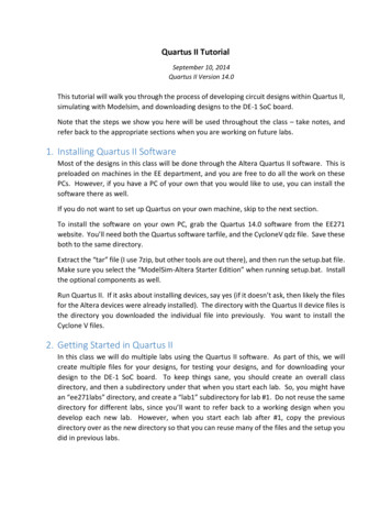
ECE 552 – Quartus TutorialFall 20092 Creating Design Projects with Quartus IIIn this section, we will learn to create a new project using Quartus II. For ease in understanding, I willgo through each and every step in designing a simple digital circuit, a 2 to 4 decoder, withaccompanying figures illustrating the step. The steps in creating a new project are as follows. Afterwe have successfully installed Quartus II and set up the license, we load the software, go to the filemenu and select ‘New Project Wizard’. This will open ‘New Project Wizard’ dialog box. The firstscreen asks us to provide names of the working directory of the project, name of the project and nameof the top level entity in the project. We will have to fill all these fields with the relevant information.Figure 1 illustrates this process.Figure 1. First screen of the ‘New Project Wizard’ dialog boxThe second screen asks us to add files to the project that we may have designed in advance. Since wedon’t have any such file to add, we will simply click next button to skip this step. Screen 2 is shownin figure 2.Page 2 of 19
ECE 552 – Quartus TutorialFall 2009Figure 2. Screen2 of the ‘New Project Wizard’ Dialog boxQuartus allows users familiar with other PLD tools to integrate their designs from those tools withQuartus II generated projects. Screen3 basically asks if there are other tools apart from Quartus II thatwe plan to use during the project. Since there are no such tools in our case, we will simply skip thisprocess by clicking ‘next’. Screen3 is shown in figure 3.Figure 3. Screen3 of the ‘New Project Wizard’Page 3 of 19
ECE 552 – Quartus TutorialFall 2009Screen4 of the wizard asks us the target device family for our project. For all projects in ECE552, wewill let the compiler select the appropriate device. This step is shown in Figure 4.Figure 4. Screen4 of the ‘New Project Wizard’Screen 5 of the ‘New Project Wizard’ asks us to specify a list of devices so that the compiler canselect one of them as the target device. For our case, default list will suffice. Screen5 is shown inFigure 5.Page 4 of 19
ECE 552 – Quartus TutorialFall 2009Figure 5. Screen5 of the ‘New Project Wizard’Finally Screen6 tells us that the ‘New Project Wizard’ is finished and the new project with the shownsettings is created. This step is shown in Figure 6.Figure 6. Screen6 of the ‘New Project Wizard’Page 5 of 19
ECE 552 – Quartus TutorialFall 2009Once we are done creating the project space, we now need to create design files for the project. Wewill use Block Diagram/Schematic File based design method throughout the course. To create a newdesign file, we go to file menu and select ‘New’ which will open the ‘New File’ Dialog box as shownin Figure 7.Figure 7. Creating a new schematic based design fileOnce we highlight the Block Diagram/Schematic File and press OK. Quartus II will open a schematiceditor with an array of tools arranged in sidebar. Figure 8 shows the toolbar holding schematic editorrelated tools. ‘Symbol Tool’ which we will use most frequently is highlighted. This tool has the shapeof an AND gate.Figure 8. Tools available with Schematic Editor where ‘Symbol Tool’ with the shape of an‘AND’ gate is highlightedPage 6 of 19
ECE 552 – Quartus TutorialFall 2009In our example of decoder design, we will use this ‘Symbol Tool’ to place all the logic elementsrequired for our decoder circuit i.e. four ‘AND’ gates and two ‘NOT’ gates as well as input and outputpins. The procedure to place any element in the schematic file is very simple, we simply select thatelement using ‘Symbol Tool’ and place it on the schematic file by the click of mouse and keep onclicking till we have placed it for the required number of times. When we are done, we just press‘ESC’ key and the mouse pointer returns to the normal arrow pointer. Figures 9-13 illustrate thisprocess.Figure 9. Selecting a 2-input ‘AND’ gate using ‘Symbol Tool’Page 7 of 19
ECE 552 – Quartus TutorialFall 2009Figure 10. Four AND gates placed on the schematic layout area.Figure 11. Selecting an ‘Input’ pin using ‘Symbol Tool’Page 8 of 19
ECE 552 – Quartus TutorialFall 2009Figure 12. Selecting a ‘NOT’ gate using ‘Symbol Tool’Figure 13. Selecting an ‘Output Pin’ Using ‘Symbol Tool’Figure 14 shows all the logic elements, without wiring, placed in the schematic file design layoutarea.Page 9 of 19
ECE 552 – Quartus TutorialFall 2009Figure 14. All logic elements required for the 2 to 4 Decoder circuit, shown placed onSchematic design layout areaFigure 15 shows how all these elements are connected to form the eventual decoder circuit.Figure 15. Schematic design of the entire 2 to 4 Decoder circuitFigure16 shows the step of saving the schematic design file. We must make sure that ‘Add file to theCurrent Project’ checkbox is in checked state while saving the file. After saving the file, we compileour project (see figure 17) and if the compilation is successful, move to the next step of simulating thecircuit which is explained in the next section.Page 10 of 19
ECE 552 – Quartus TutorialFall 2009Figure 16. Saving the schematic file, make sure that ‘Add File to current project’checkbox is in checked stateFigure 17. Compiling the schematic designPage 11 of 19
ECE 552 – Quartus TutorialFall 20093 Simulating Designed Circuits Using QuartusIn this section, we will follow the same step by step illustrative approach to go through each steprequired to perform simulation of the decoder circuit in the previous section. First step is to create anew Simulation Input file. We will use the “Vector Waveform File’ format to define simulationinputs. To create a new ‘Vector Waveform file’ we first go to file menu, select ‘New’ and then select‘Vector Waveform File’ in the ‘Other Files’ tab on the ‘New File’ Dialog box. The step is shown inFigure18.Figure 18. ‘New File’ Dialog box for creating a new simulation file based upon ‘VectorWaveform File’ formatAfter pressing OK on the “New File’ Dialog box, we go to the ‘View’ menu, select ‘Utility Windows’and then select ‘Node Finder’ as shown in Figure19.Page 12 of 19
ECE 552 – Quartus TutorialFall 2009Figure 19. Selecting the ‘Node Finder’ toolWe will use ‘Node Finder’ to select input nodes of our newly designed circuit. What I have done hereis to simply ask it to list all nodes by using the filter pins: all as illustrated in Figure20.Figure 20. The input and output nodes enumerated by ‘Node Finder’ toolOnce it shows all the pins I select the input ones (represented by a preceding i on a pin shape) anddrag them to the vector waveform file designated area for inputs as shown in Figure21.Page 13 of 19
ECE 552 – Quartus TutorialFall 2009Figure 21. Dragging input nodes onto the simulation input file.Once we have dragged the input nodes on the Vector Waveform file, we will use the ‘WaveformEditing Tool’ (shown highlighted!in Figure22) to create simulations waveforms for the inputs. Forthis, we simply select the ‘Waveform Editing Tool’ and drag it on the waveform area correspondingto the input for which we want to generate the waveform. Just by dragging mouse pointer, afterselecting this tool, on the waveform area we cans switch between logic low and logic high levels asshown in Figure23. Finally once we have generated the waveforms corresponding to all inputs (two incase of decoder) (Figure24) we save the simulation file (Figure25).Figure 22. The ‘Waveform Figure 23. Using ‘Waveform Editing Tool’ to create waveforms forEditing Tool’ highlightedinput nodes A and BFigure 24. The simulation waveforms for inputs A and BPage 14 of 19
ECE 552 – Quartus TutorialFall 2009Figure 25. Saving the ‘Vector Waveform File’ format basedsimulation input file for decoder circuit.Figure26. “Start Simulation’button highlightedAfter saving the simulation input ‘Vector Waveform File’. We perform simulation bypressing the ‘Start Simulation’ button (shown highlighted in Figure26).Once simulation is donesuccessfully, we can see output waveforms corsesponding to output pins on the VectorWaveform File as shown in Figure27Figure 27. Simulation ResultsPage 15 of 19
ECE 552 – Quartus TutorialFall 20094 Hierarchical Design and Buses Using QuartusIn this section, we will follow a similar step-by-step illustrative approach to learn how to performhierarchical design and how to use buses in our design. First, make sure the demo.bdf schematic isopen, then we need to save a copy, e.g., File saveas 2to4.bdf. Then, make sure this file is openin the design window. Delete the nets connecting the inputs and outputs to the rest of the circuitry,and also delete all but one of the inputs and outputs. The results are shown in figure 28.Figure 28.Rename the input as ‘A[1.0]’ and the output as ‘CS[3.0]’. You can easily do this by putting themouse over the object, right-clicking, selecting ‘properties’, and changing the name. Add a bus tothe input and a bus to the output. Do this by selecting the bus symbol (like the net symbol butwith a thicker line) and drawing the bus lines. The results are shown in figure 29.Figure 29.Page 16 of 19
ECE 552 – Quartus TutorialFall 2009Now select the net tool and add nets from the NOT gate inputs to the input bus and from the ANDgate outputs to the output bus. Name the buses and nets by right-clicking on each in turn,selecting ‘properties’ and changing the name. See figure 30 for the name assignments.Figure 30.Save the design file. Now we need to make a symbol file for use in schematics. Do File Create/update Create symbol file to save 2to4 as a symbol.Now, open demo.bdf again. Delete the circuit logic symbols and the nets, as well as all inputs andoutputs except one of each. Rename the input to A[3.0] by doing a {right-click} Propertiesand changing the name. Repeat the procedure to change the output to CS[7.0]. Your schematicshould look like that of figure 31.Figure 31.Now we need to add two 2to4 decoder symbols using the decoder we designed earlier. In thetoolbar, select the ‘symbol’ key and in the dialog box that comes up, select Project 2to4 then‘OK’. This dialog is shown in figure 32.Page 17 of 19
ECE 552 – Quartus TutorialFall 2009Figure 32.Place two copies of the 2to4 decoder in the schematic and hit ‘Esc’. Your schematic should looklike figure 33.Figure 33.Add buses to the input and to the output and connect to the decoders with sub-buses. Select eachsegment of the buses in turn, then {right-click} Properties and name them to match figure 34.Page 18 of 19
ECE 552 – Quartus TutorialFall 2009Figure 34.Save the file. Now we need to set this as the top-level entity. In the ‘Project Navigator’ area,select demo.bdf and {right-click} set as top-level entity.Congratulations! You are now a Quartus II expert!Page 19 of 19
ECE 552 – Quartus Tutorial Fall 2009 Page 2 of 19 2 Creating Design Projects with Quartus II In this section, we will learn to create a new project using Quartus II. For ease in understanding, I will go through each and every step in designing a simple digital circuit, a 2 to 4
