Transcription
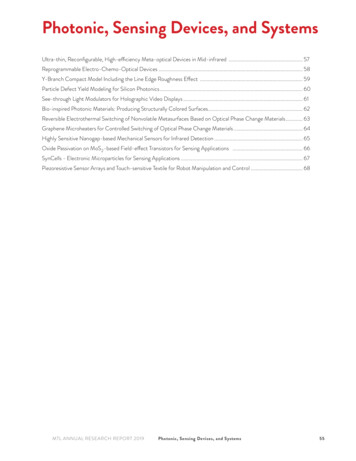
Photonic, Sensing Devices, and SystemsUltra-thin, Reconfigurable, High-efficiency Meta-optical Devices in Mid-infrared . 57Reprogrammable Electro-Chemo-Optical Devices. 58Y-Branch Compact Model Including the Line Edge Roughness Effect . 59Particle Defect Yield Modeling for Silicon Photonics. 60See-through Light Modulators for Holographic Video Displays. 61Bio-inspired Photonic Materials: Producing Structurally Colored Surfaces. 62Reversible Electrothermal Switching of Nonvolatile Metasurfaces Based on Optical Phase Change Materials. 63Graphene Microheaters for Controlled Switching of Optical Phase Change Materials. 64Highly Sensitive Nanogap-based Mechanical Sensors for Infrared Detection. 65Oxide Passivation on MoS2-based Field-effect Transistors for Sensing Applications . 66SynCells - Electronic Microparticles for Sensing Applications. 67Piezoresistive Sensor Arrays and Touch-sensitive Textile for Robot Manipulation and Control. 68MTL ANNUAL RESEARCH REPORT 2019Photonic, Sensing Devices, and Systems55
56Photonic, Sensing Devices, and SystemsMTL ANNUAL RESEARCH REPORT 2019
Ultra-thin, Reconfigurable, High-efficiency Meta-optical Devices in Mid-infraredM. Y. Shalaginov, S. An, Y. Zhang, P. Su, A. Yadav, M. Kang, C. Rios, A. Agarwal, K. Richardson, H. Zhang, T. Gu, J. HuSponsorship: DARPA EXTREME ProgramThe mid-infrared (MIR) is a frequency band strategically important for numerous biomedical, military,and industrial applications. Further development ofMIR devices is hindered by the lack of inexpensive andefficient basic optical elements such as lenses, waveplates, filters, etc. Furthermore, the available components are typically bulky and passive. Our research addresses these challenges by leveraging novel low-lossoptical phase-change materials (Ge-Sb-Se-Te) and theirsub-wavelength patterning to achieve ultra-thin (thickness 0/5), high-efficiency ( 25%), and multi-functional MIR components.As a proof-of-principle, we demonstrated areconfigurable bifocal meta-lens with a switchablefocus. Our metalens principle is based on collective Miescattering of incident plane waves by subwavelengthdielectric structures, which sustain both electric andmagnetic dipolar resonances. Each of the scatterers,also known as Huygens’ meta-atoms, contributesto the phase and amplitude of the incident beam.The amount of phase shift was controlled by themeta-atom geometry and its refractive index. Properspatial arrangement of meta-atoms can reconstruct adesired phase profile. For instance, lens functionalitycan be achieved by introducing a hyperboloid phasedistribution. In amorphous state (A-state) the lensfocuses the incident light at a focal length of 1 mm;after the heating-induced material state transition, thefocal length changes to 1.5 mm (C-state). The switchingof the focal length was attained by changing thehyperboloidal phase profiles.For simplicity, we performed binary discretizationof original continuous phase distributions: 0 and 180 phase shifts. Then, we formed a library of four distinctmeta-atoms that can realize the binary transitions.The metalens was fabricated by depositing a 1-m-thickGe2Sb2Se4Te1 film onto CaF2 substrate followedby patterning processes involving electron-beamlithography patterning and reactive ion etching witha mixture of fluoromethane gases. We believe that ourfindings will enable a new range of compact, multifunctional spectroscopic, and thermal imaging devices. Figure 1: Illustration of reconfigurable meta-lens, with properties that can be switched by transitioning non-volatile phase-change material (GeSbSeTe) from amorphous (A) to crystalline (C) state.FURTHER READING Y. Zhang, J. B. Chou, J. Li, H. Li, Q. Du, A. Yadav, S. Zhou, M. Y. Shalaginov, Z. Fang, H. Zhong, C. Roberts, P. Robinson, B. Bohlin, C. Ríos, H. Lin,M. Kang, T. Gu, J. Warner, V. Liberman, K. Richardson, and J. Hu, “Extreme Broadband Transparent Optical Phase Change Materials for Highperformance Nonvolatile Photonics,” arxiv:1811.00526, 2018.L. Zhang, J. Ding, H. Zheng, S. An, H. Lin, B. Zheng, Q. Du, G. Yin, J. Michon, Y. Zhang, Z. Fang, M. Y. Shalaginov, L. Deng, T. Gu, H. Zhang, and J. Hu,“Ultra-thin High-efficiency mid-Infrared Transmissive Huygens Meta-optics,” Nat. Commun. vol. 9, p. 1481, 2018.MTL ANNUAL RESEARCH REPORT 2019Photonic, Sensing Devices, and Systems57
Reprogrammable Electro-Chemo-Optical DevicesD. Kalaev, H. L. TullerSponsorship: U.S. Department of Energy, Basic Energy Sciences ProgramPhotonic devices with programmable properties allowmore flexibility in the manipulation of light. Recently,several examples of reconfigurable photonic deviceswere demonstrated by controlling the local/overall index of refraction in thin films, either by a thermallyinduced phase change in chalcogenides or by intercalation of lithium into oxides. We propose a novel approach for design of reprogrammable photonic devicesbased on electrochemical modification of ceria-basedelectro-chemo-optical devices.Previously, it was shown that the refractive Figure 1a: Nonvolatile change in the optical transmissionof PrxCe1-xO2-δ (PCO) thin film by electrochemical oxygenpumping. a. Oxygen pumped into the PCO thin film by anapplied positive bias, resulting in the low optical transmission.58index of PrxCe1-xO2-δ (PCO) is a function ofoxygen nonstoichiometry δ , that can be controlledelectrochemically via closely spaced electrodes in alateral device configuration. For transverse modifiedconfigurations, a PCO thin film on yttrium-stabilizedzirconia (YSZ) substrate with transparent conductingoxide (TCO) top electrode allows for voltage-controlledoxygen exchange. Enhanced spatial resolution canbe further achieved with the aid of lithographicallypatterned nano-dimensioned oxide layers. Figure 1b: Oxygen pumped out of the PCO thin film byan applied negative bias, resulting in the high optical transmission.Photonic, Sensing Devices, and SystemsMTL ANNUAL RESEARCH REPORT 2019
Y-Branch Compact Model Including the Line Edge Roughness EffectS. I. El-Henawy, D. S. BoningSponsorship: AIM PhotonicsSilicon photonics is a booming design platform due toits ability to support high data rates and enable novelapplications. Since the CMOS fabrication infrastructure is leveraged in silicon photonics, it becomes crucialto provide process-variation-aware compact modelsas optical components inherit the process variationsfound in CMOS. These models would help designers,enhance yield, and serve as a building block in the silicon photonics process design kit (PDK).We develop a compact model for a basic photoniccomponent, a Y-branch, that specifies the variationsin the transfer characteristics against line-edgeroughness (LER). LER is a common statistical randomprocess variation that causes imbalanced transmissionbetween the two output ports of the Y-branch, whichis supposed to be balanced. As a random processvariation, LER affects the Y-branch transmission in arandom behavior, so the transmission can be describedby its mean (µ) and variance (σ2). This model providesthe transmission mean and variance as a function ofLER parameters, amplitude (A) and correlation length(LC), across the operating wavelength range of interest(λ).The flow of modeling, shown in Figure 1, startsby simulating different A and LC combinations withmultiple instantiations for each to get a statistical senseof the variations. Afterward, the optical behavior of theY-branch with the imposed LER is extracted and usedto develop the compact model. The model is developedusing the Gaussian process regression method wherethe R2 score for both mean and variance predictions is0.99. Figure 2 shows the model’s performance on testdata for predicting mean and variance. This modelcan be used in photonic integrated circuit simulatorsto predict the performance across process variationsand worst corner cases as the models we rely upon inCMOS design. Figure 1: Simulation flow used to develop a statistical compact model that includes the LER effect.WWFigure 2: Mean and variance prediction for test data using aGaussian process regression model across the wavelength ofinterest.FURTHER READING S. I. El-Henawy, R. Miller, and D. S. Boning, “Effect of a Random Process Variation on the Transfer Characteristics of a Fundamental PhotonicIntegrated Circuit Component,” SPIE Optics and Photonics, vol. 10743, p. 107430O-1, 2018.L. Chrostowski and M. Hochberg, “Silicon Photonics Design: From Devices to Systems,” Cambridge: Cambridge University Press, 2015.MTL ANNUAL RESEARCH REPORT 2019Photonic, Sensing Devices, and Systems59
Particle Defect Yield Modeling for Silicon PhotonicsZ. Zhang, M. B. McIlrath, D. S. BoningSponsorship: AIM PhotonicsSilicon photonics, where photons instead of electronsare manipulated, shows promise for higher data rates,lower energy communication and information processing, biomedical sensing, and novel optically based functionality applications such as wavefront engineeringand beam-steering of light. In silicon photonics, bothelectrical and optical components can be integrated onthe same chip, using a shared silicon integrated circuit(IC) technology base. However, silicon photonics doesnot yet have a mature process, device, and circuit variation models for the existing IC and photonic processsteps; this lack presents a key challenge for design inthis emerging industry.Our goal is to develop key elements of a robustdesign for manufacturability methodology for siliconphotonics. As one part of the goal, here we focus on theimpact of particle defects in silicon photonics, whichcan arise in photolithography, deposition, etching, andother processes. The model and result will be usedto help generate layout design rules and critical areaextraction methods, predicting and optimizing theyield of complex silicon photonic devices and circuitsfor tomorrow’s silicon photonics designers, just as ICdesigners do today.We model the impact of different types of particledefects (Figure 1) on different device components, e.g.,straight waveguides (Figure 2) and y-splitters (Figure3). We modify and apply the adjoint method, which iswidely used in optimization, to accelerate the speedof simulation and reduce numerical error. The resultfrom the adjoint method shows good consistency withdirect simulation over different types of particles,different device components, and wavelengths rangingfrom 1500 to 1600 nm. The same methodology can beused on the circuit level and thus predict the yield ofthe chip. Present research also focuses on generatinglayout design rules and critical area extraction basedon results from the adjoint method. Figure 1: Examples of modeling of particle defects: (a) silicon pillar photolithography defect and (b) metal ball for foreignmetal particle. Figure 2: Phase shift impact of a dioxide pillar hole of radius40 nm on a straight silicon waveguide, from both direct simulation and adjoint methods. Distance is measured from the centerof the waveguide to the center of the particle. Figure 3: Mapping of transmission impact of a dioxide pillarhole of radius 40 nm on a y-splitter, as the function of the location of the defect, predicted by the adjoint method.FURTHER READING 60Z. Zhang, S. I. El-Henawy, A. Sadun, R. Miller, L. Daniel, J. K. White, and D. S. Boning, “Adjoint-based Sensitivity Analysis for Silicon PhotonicVariations,” 2019 IEEE MTT-S International Conference on Numerical Electromagnetic and Multiphysics Modeling and Optimization (NEMO),Cambridge MA, 2019.L. Chrostowski and M. Hochberg, “Silicon Photonics Design: from Devices to Systems,” Cambridge: Cambridge University Press, 2015.Photonic, Sensing Devices, and SystemsMTL ANNUAL RESEARCH REPORT 2019
See-through Light Modulators for Holographic Video DisplaysS. Jolly, T. Schoeppner, B. Datta, V. M. Bove, Jr. in collaboration with Daniel Smalley (Brigham Young University)Sponsorship: MIT Media Lab Research Consortium, U.S. Air Force Research LaboratoryIn this research, we design and fabricate acousto-optic,guided-wave modulators in lithium niobate for use inholographic and other high-bandwidth displays. Guided-wave techniques make possible the fabrication ofmodulators that are higher in bandwidth and lower incost than analogous bulk-wave acousto-optic devicesor other spatial light modulators used for diffractivedisplays; these techniques enable simultaneous modulation of red, green, and blue light.We are investigating multichannel variants ofthese devices with an emphasis on maximizing thenumber of modulating channels to achieve largetotal bandwidths. To date, we have demonstratedmultichannel full-color modulators capable ofdisplaying holographic light fields at standarddefinition television resolution and video frame rates.Our current work explores a device architecturesuitable for wearable augmented reality displays andother see-through applications, in which the lightoutcouples toward the viewer (Figure 1), fabricatedusing femtosecond laser micromachining (Figure 2). Figure 1: Diagram of near-eye version of our device. Figure 2: Metal features, waveguides, and reflection gratings fabricated using femtosecond laser processing.FURTHER READING S. Jolly, N. Savidis, B. Datta, D. Smalley, and V. M. Bove, Jr., “Progress in Transparent, Flat-panel Holographic Displays Enabled by Guided-waveAcousto-optics,” Proc. SPIE Practical Holography XXXII: Displays, Materials, and Applications, p. 10558, 2018.S. Jolly, N. Savidis, B. Datta, T. Karydis, W. Langford, N. Gershenfeld, and V. M. Bove, Jr., “Progress in Fabrication of Anisotropic Bragg Gratingsin Lithium Niobate via Femtosecond Laser Micromachining,” Proc. SPIE Advanced Fabrication Technologies for Micro/Nano Optics andPhotonics XI, p. 10554, 2018.MTL ANNUAL RESEARCH REPORT 2019Photonic, Sensing Devices, and Systems61
Bio-inspired Photonic Materials: Producing Structurally Colored SurfacesB. Datta, S. Jolly, V. M. Bove, Jr.Sponsorship: MIT Media Lab Research ConsortiumAdvances in science and engineering are bringing uscloser and closer to systems that respond to humanstimuli in real time. Scientists often look to biology forexamples of efficient, spatially tailored multifunctionalsystems, drawing inspiration from photonic structureslike multilayer stacks similar to those in the morphobutterfly. In this project, we develop an understanding of the landscape of responsive, bio-inspired, andactive materials, drawing on principles of photonicsand bio-inspired material systems. We are exploringmaterial processing techniques (starting with electronbeam lithography and moving to direct laser writing)to produce and replicate structurally colored surfaceswhile developing simulation and modeling tools (suchas inverse design processes) to generate new structuresand colors. Such complex biological systems requireadvanced fabrication techniques. Our designs are realizable through fabrication using direct laser writingtechniques such as two-photon polymerization. Weaim to compare our model system and simulations tofabricated structures using optical microscopy, scanning electron microscopy, and angular spectrometry.This process provides a toolkit with which to examineand build other bio-inspired, tunable, and responsivephotonic systems and expand the range of achievablestructural colors.Unlike with natural structures, producingbiomimetic surfaces allows researchers to testbeyond tunability that occurs naturally and explorenew theory and models to design structures withoptimized functions. The benefits of such biomimeticnanostructures are plentiful: they provide brilliant,iridescent color with mechanical stability and lightsteering capabilities. By producing biomimeticnanostructures, designers and engineers can capitalizeon unique properties of optical structural color andexamine these structures based on human perceptionand response. Figure 1: “Tree-like” structures replicating the ridge structure Figure 2: Color responses generated with incident reflecof morpho butterflies, fabricated in poly (methyl methacrylate) tive illumination using a broadband light source, demonstratingon silicon using electron beam lithography.proof-of-principle optical response.FURTHER READING 62B. C. Datta, S. K. Jolly, and V. M. Bove, “Towards Inverse Design of Biomimetic Nanostructures Exhibiting Composite Structural Coloration,” Proc.SPIE Advanced Fabrication Technologies for Micro/Nano Optics and Photonics XII, vol. p. 10930, 2019.R. H. Siddique, S. Diewald, J. Leuthold, and H. Hölscher, “Theoretical and Experimental Analysis of the Structural Pattern Responsible for theIridescence of Morpho Butterflies,” Optics Express, vol. 21, p. 12, pp. 14351-14361, 2013.G. Zyla, A. Kovalev, M. Grafen, E. L. Gurevich, C. Esen, A. Ostendorf, and S. Gorb, “Generation of Bioinspired Structural Colors via Two-photonPolymerization,” Scientific Reports, vol. 7, no. 1, p. 17622, 2017.Photonic, Sensing Devices, and SystemsMTL ANNUAL RESEARCH REPORT 2019
Reversible Electrothermal Switching of Nonvolatile Metasurfaces Based on OpticalPhase Change MaterialsY. Zhang, J. Liang, M. Shalaginov, S. Deckoff-Jones, C. Ríos, J. B. Chou, C. Roberts, S. An, C. Fowler, S. D. Campbell, B. Azhar, C.Gonçalves, K. Richardson, H. Zhang, D. H. Werner, T. Gu, J. HuSponsorship: DARPA ASD (R&E )Chalcogenide phase change materials (PCMs) are highly attractive for active metasurface applications due totheir nonvolatile switching capability. So far, reversible switching of PCM-based metasurfaces is realizedvia either laser pulsing or electrical-current-inducedphase transition. Both methods require raster-scannedwriting and bulky off-chip instruments (lasers or AFMsetups), making them incompatible with large-scale onchip integration. A robust and scalable, on-chip, PCMbased metasurface switching method is therefore highly desired. Here we report an electrothermal switchingmethod employing on-chip metal heaters, enablinglarge-area reversible switching for PCM-based metasurfaces.Figure 1a shows the optical constants of thelow-loss optical PCM (O-PCM) we choose for thisapplication: Ge2Sb2Se4Te1 (GSST), which exhibits lowloss at both its amorphous and crystalline phasesover a broad spectral range. Moreover, its improvedamorphous phase stability gives rise to a larger criticalswitching thickness than that of traditional PCMs (e.g.,GST-225). These two factors make GSST a preferredmaterial for metasurface applications. Figure 1billustrates the design of the switching platform.Ti/Pt are used as a metal heater for its excellentconductivity. After an atomic layer deposition ofAl2O3, GSST is subsequently deposited and patternedvia electron beam lithography. The thickness of theGSST meta-atoms is designed to be 220 nm. Finally, aSiO2 capping layer is deposited to prevent oxidationand evaporation of the PCM. The devices are wirebonded onto a custom printed circuit board carrier toenable in-situ Raman and Fourier transform infrared(FTIR) characterizations. Figure 1c shows the SEM andoptical microscope images of a fabricated device. Theboundary of the heat is optimized for uniform heatingin the PCM area. Figure 1d confirms the completereversible switching of the PCM utilizing the distinctRaman peaks of amorphous and crystalline states.Figure 1e shows that more than 40% reflection contrastis achieved using this platform. Figure 1f, on the otherhand, demonstrates that applying different voltagescan achieve any arbitrary levels of crystallization,therefore providing possibilities for quasi-continuoustuning using this platform. Figure 1: (a) Optical properties of a- (black) and c- (red) state GSST alloys; (b) Sketch of the device; (c) Optical and scanningelectron microscope images of the device; (d) Raman spectra of as-deposited, crystallized and re-amorphized PCM metasurfaces;(e) FTIR response of a device in its a- and c- states after 35 cycles of switching; (f) Demonstration of quasi-continuous switching.FURTHER READING Y. Zhang, J. B. Chou, J. Li, H. Li, Q. Du, J. Hu, et al., “Extreme Broadband Transparent Optical Phase Change Materials for High-performanceNonvolatile Photonics,” [online], arXiv preprint arXiv:1811.00526, 2018.Y. Zhang, J. Liang, M. Shalaginov, S. Deckoff-Jones, C. Ríos, J. Chou, C. Roberts, S. An, et al., “Electrically Reconfigurable Nonvolatile Metasurfaceusing Optical Phase Change Materials,” Conference on Lasers and Electro-Optics, OSA Technical Digest (Optical Society of America, 2019 ), p.JTh5B.3, 2019.MTL ANNUAL RESEARCH REPORT 2019Photonic, Sensing Devices, and Systems63
Graphene Microheaters for Controlled Switching of Optical Phase Change MaterialsC. Ríos, Y. Zhang, S. Deckoff-Jones, M. Shalaginov, H. Wang, H. Li, J. Kong, T. Gu, J. HuSponsorship: Defense Advanced Research Projects Agency Extreme ProgramThe integration of optical phase change materials(O-PCMs) into photonic devices enables a long-soughtfunctionality: nonvolatile reconfiguration, the abilityto switch between at least two distinct configurationswith no power consumption to retain either one. Energy-efficient, highly cyclable integrated optical devicessuch as switches, memories, metasurfaces, color pixels,and brain-inspired computing elements are successful examples of O-PCMs applications. However, theseresults use optical switching mechanisms that arechallenging to scale up for architectures comprisinghundreds of large-area active cells. To tackle this challenge, we present a hybrid electro-optical frameworkin which we use graphene microheaters for thermalswitching of Ge2Sb2Se4Te1 (GSST). We choose GSST because of its broadband transparency in the infrared beyond 18.5-µm wavelengths in both the amorphous andthe crystalline states. Similarly, we choose graphene forour integrated approach because of its minimal opticalloss ( 0.1–1.2 dB/mm), high thermal conductivity, andstability. Such a device benefits from scalable electricalcontrol, while having a reconfigurable optical response.We demonstrate large-area switching of 50-nmthick, 4 3-µm2 GSST using a 5 10-µm2 grapheneheater (Figures 1A and 1B). The chip was wire-bondedonto a printed circuit board to enable in-situ Ramanprobing while electrically testing each integrateddevice (Figures 1C and D). To switch the as-depositedGSST to the crystalline state (heat up over 280 C), weused 6V pulses with varying lengths between 10-20ms. To reamorphize (melt over 650 C and quench), wetriggered 13-µs electrical pulses with a peak voltage of7.5V. We demonstrate repeatable electrical switchingby in-situ Raman spectroscopy of GSST after each pulseexcitation (Figure 1E), done by tracking the amorphousand crystalline signature peaks at 159 cm-1 and120cm-1, respectively (Figure 1F). Furthermore, thechange in color observed in the inset microscope imagesof Figure 1F demonstrates the nonvolatile modulationof the optical properties upon GSST switching. Figure 1: A sketch of a reconfigurable PCM device using a graphene heater. B. Optical microscope image ofthe device. C. Switchable wire-bonded device arrays. D. Assembly inside a Raman microscope using long workingdistance objectives. E. Demonstration of 10 switching events by measuring the Raman signal (RS) at the characteristic peaks of both states. F. Raman spectra of GSST for the four points highlighted in E.FURTHER READING 64M. Wuttig, H. Bhaskaran, and T. Taubner, “Phase-change Materials for non-Volatile Photonic Applications,” Nat. Photonics, vol. 11, pp. 465–476,2017.C. Ríos, Y. Zhang, S. Deckoff-Jones, H. Li, J.B. Chou, H. Wang, M. Shalaginov, C. Roberts, C. Goncalves, V. Liberman, T. Gu, H. Wang, T. Gu, J. Kong, K.Richardson, and J. Hu, “Reversible Switching of Optical Phase Change Materials using Graphene Microheaters,” CLEO Science and Innovations,paper SF2H.4, 2019.Photonic, Sensing Devices, and SystemsMTL ANNUAL RESEARCH REPORT 2019
Highly Sensitive Nanogap-based Mechanical Sensors for Infrared DetectionY. Lin, X. Ji. R. J. Catalano, E. N. Tas, J. Han, J. H. Lang, F. Niroui, J. Kong, T. PalaciosSponsorship: Army Research Office MIT-ISN, Air Force Office of Scientific Research-MURIMany new physical phenomena show up only on nanoscale structures; with these phenomena, we candesign novel devices with unprecedented functionality. Nanoengineering makes it possible to fabricationnanometer-sized quantum tunneling barriers that canbe tuned mechanically. Such a tremendous mechanicaltunability can be harnessed for mechanical sensors andmany other types of sensors with extremely high sensitivity.Here we demonstrate two nanostructures thatimplement such a mechanically tunable tunnelingbarrier and use them for either a mechanical/strainsensor or a mid-infrared bolometric detector. Thefirst nanostructure is the self-assembled graphene Figure 1: Nanogap based mechanical/strain sensors. (a) Schematic of graphene nanoflake network. (b) Schematic of metal/SAM/metal nanogap structure. (c) Measured maximum gaugefactors (GFmax) of graphene nanoflake network and metal/SAM/metal structure vs. state of the art .MTL ANNUAL RESEARCH REPORT 2019nanoflake network (Figure 1 (a)). It is composed of aresistance network of sub-micron graphene flakesthat connect with 100 nm overlap. The secondnanostructure is a metal nanogap with the gap definedby self-assembled monolayers (SAMs) (Figure 1 (b)).The proposed structures show high gauge factorsand/or improved linear dynamic range as strainsensors (Figure 1 (c)). Such mechanical sensors canalso be integrated with a thermal actuator to realizea highly sensitive, uncooled bolometer-type midinfrared detector (Figure 2(a) and (b)). The measuredtemperature coefficient of resistance (TCR) can beas high as 5 K-1, which is more than one order ofmagnitude better than the state of the art (Figure 2(c)). Figure 2: Thermo-mechanical bolometric mid-IR detectors.(a) Schematic of device composed of nanogap-based mechanical sensing component (black), thermal actuator (grey), and rigidframe (green). (b) Optical microscopic image of as-fabricateddevice. (c) Measured maximum TCR (TCRmax) vs. state of the art.Photonic, Sensing Devices, and Systems65
Oxide Passivation on MoS2-based Field-effect Transistors for Sensing ApplicationsM. Xue, T. PalaciosSponsorship: MIT-ARL ISN, NSF CIQMTwo-dimensional materials have attracted much attention as candidates for next-generation sensingplatforms because of their unique electrical, optical,mechanical, and chemical properties. Due to its naturalbandgap, MoS2 is one of the most popular two-dimensional materials for sensing. The sensing signal can beamplified as charges transfer onto the MoS2 channeland result in strong modulations in current with thepresent of the analyte. The large surface-to-volume ratio also contributes to the high sensitivity of a MoS2based sensor. However, high sensitivity also results inmuch noise as vapor molecules and other interferingmolecules absorb on the exposed MoS2 surface. Also,unprotected MoS2 can degrade in an ambient environment due to oxidation and surface contaminants.Therefore, a suitable passivation layer is needed to protect the channel surface but still preserve the sensitivity of MoS2.In this work, back-gated MoS2 field-effecttransistors (FETs) were fabricated, and a thin layer of Figure 1: Output characteristic of oxide-passivated MoS2FETs. The inset shows the device structure.Al2O3 was deposited to passivate the channel surface.Prior to atomic layer deposition of Al2O3 as a seed layer,2 nm of aluminum was deposited. Approximately 13 nmof Al2O3was added to the final device. With the oxidepassivation, the hysteresis of both output and transfercharacteristics was greatly reduced, indicatingeffective protection from fast absorbent-type trappingsite.The sensing ability of oxide-passivated MoS2FETs was also tested with a series of the electrolytesolution of pH ranging from 5 to 10. As shown inFigure 2, a near-linear relationship between relativechange in resistance and change in pH was achieved.This work proves that Al2O3is a great passivationlayer for MoS2-based sensor devices. With oxide beingthe outmost layer, other oxide-compatible surfacefunctionalization can also be used to improve theselectivity of such sensors while still benefiting fromMoS2’s natural sensitivity. Figure 2: Relative change in channel resistance as functionof pH values of electrolyte. The channel size is 50 µm x 10 µm,Vgs 0V.FURTHER READING 66Y. Y. Illarionov, K. K. H. Smithe, M. Waltl, T. Knobloch, E. Pop, and T. Grasser, “Improved Hysteresis and Reliability of MoS2Transistors with Highquality CVD Growth and Al2O3Encapsulation,” IEEE Electron Device Lett., vol. 38, no. 12, pp. 1763–1766, 2017.A. Sinha, Dhanjai, B. Tan, Y. Huang, H. Zhao, X. Dang, J. Chen, and R. Jain, “MoS2 Nanostructures for Electrochemical Sensing of MultidisciplinaryTargets: A Review,” TrAC Trends Anal. Chem., vol. 102, pp. 75–90, May 2018.Photonic, Sensing Devices, and SystemsMTL ANNUAL RESEARCH REPORT 2019
SynCells - Electronic Microparticles for Sensing ApplicationsM. Hempel, V. Schröder, C. Park, M. Xue, J. Park, T. Swager, J. Kong, T. PalaciosSponsorship: Air Force Office of Scientific ResearchAlthough tra
Integrated Circuit Component," SPIE Optics and Photonics, vol. 10743, p. 107430O-1, 2018. L. Chrostowski and M. Hochberg, "Silicon Photonics Design: From Devices to Systems," Cambridge: Cambridge University Press, 2015. Silicon photonics is a booming design platform due to its ability to support high data rates and enable novel
