Transcription
IEEE JOURNAL OF SELECTED TOPICS IN QUANTUM ELECTRONICS, VOL. 25, NO. 5, SEPTEMBER/OCTOBER 20198200818Open-Access Silicon Photonics Platforms in EuropeAbdul Rahim , Jeroen Goyvaerts, Bertrand Szelag , Jean-Marc Fedeli , Philippe Absil, Timo Aalto ,Mikko Harjanne , Callum Littlejohns , Graham Reed, Georg Winzer, Stefan Lischke, Lars Zimmermann,Dieter Knoll, Douwe Geuzebroek , Arne Leinse, Michael Geiselmann, Michael Zervas, Hilde Jans, Andim Stassen,Carlos Domínguez , Pascual Muñoz , Senior Member, IEEE, David Domenech, Anna Lena Giesecke ,Max C. Lemme , Senior Member, IEEE, and Roel Baets , Fellow, IEEE(Invited Paper)Abstract—Offering open-access silicon photonics-based technologies has played a pivotal role in unleashing this technologyfrom research laboratories to industry. Fabless enterprises rely onthe open-access of these technologies for their product development. In the last decade, a diverse set of open-access technologieswith medium and high technology readiness levels have emerged.This paper provides a review of the open-access silicon and silicon nitride photonic IC technologies offered by the pilot lines ofManuscript received January 3, 2019; revised March 18, 2019; accepted April26, 2019. Date of publication May 10, 2019; date of current version June 6, 2019.(Corresponding author: Abdul Rahim.)A. Rahim, J. Goyvaerts, and R. Baets are with the Photonics Research Group,Department of Information Technology, Ghent University—imec and Center forNano- and Biophotonics, Ghent University, Ghent B-9000, Belgium (e-mail:abdul.rahim@ugent.be; jeroen.goyvaerts@ugent.be; roel.baets@ugent.be).B. Szelag and J.-M. Fedeli are with the Commissariat à l’Energie Atomique et aux Energie Alternatives, University Grenoble Alpes and CEA, LETI,F-38054, Grenoble Cedex, France (e-mail: bertrand.szelag@cea.fr; jean-marc.fedeli@cea.fr).P. Absil, H. Jans, and A. Stassen are with the Imec, 3001 Leuven, Belgium(e-mail: absilp@imec.be; hilde.jans@imec.be; andim.stassen@imec.be).T. Aalto and M. Harjanne are with VTT, FI-02044 Espoo, Finland (e-mail:timo.aalto@vtt.fi; mikko.harjanne@vtt.fi).C. Littlejohns and G. Reed are with the Optoelectronics Research Centre, University of Southampton, Southampton SO17 1BJ, U.K. (e-mail:c.littlejohns@soton.ac.uk; g.reed@soton.ac.uk).G. Winzer, S. Lischke, and D. Knoll are with IHP Leibniz-Institut fürinnovative Mikroelektronik, 15236 Frankfurt, Germany (e-mail: winzer@ihp-microelectronics.com; lischke@ihp-microelectronics.com; Knoll@ihpmicroelectronics.com).L. Zimmermann is with IHP Leibniz-Institut für innovative Mikroelektronik,15236 Frankfurt, Germany, and also with the Siliziumphotonik, Institut fürHochfrequenz- und Halbleiter - Systemtechnologien, Fakultät IV, 10587 Berlin,Germany (e-mail: lzimmermann@ihp-microelectronics.com).D. Geuzebroek and A. Leinse are with the LioniX International BV,Enschede, The Netherlands (e-mail: d.h.geuzebroek@lionix-int.com; a.leinse@lionix-int.com).M. Geiselmann and M. Zervas are with LIGENTEC, 1015 Lausanne,Switzerland (e-mail: michael.geiselmann@ligentec.com; michael.zervas@ligentec.com).C. Domínguez is with the Instituto de Microelectrónica de Barcelona(IMB-CNM, CSIC), 08193 Bellaterra, Spain (e-mail: carlos.dominguez@imb-cnm.csic.es).P. Muñoz is with the Photonics Research Labs, Universitat Politécnica deValencia, 46021 Valencia, Spain (e-mail: pascual.munoz@upv.es).D. Domenech is with the VLC Photonics S.L., 46021 Valencia, Spain (e-mail:jose.domenech@vlcphotonics.com).A. L. Giesecke is with AMO GmbH, 52074 Aachen, Germany (e-mail:giesecke@amo.de).M. C. Lemme is with RWTH Aachen University and AMO GmbH, 52074Aachen, Germany (e-mail: lemme@amo.de).Color versions of one or more of the figures in this paper are available onlineat http://ieeexplore.ieee.org.Digital Object Identifier 10.1109/JSTQE.2019.2915949European research institutes and companies. The paper also highlights upcoming features of these platforms and discusses how theyaddress the long-term market needs.Index Terms—Silicon photonics, Silicon-on-Insulator, SiliconNitride, CMOS, foundry, open-access, photonic integrated circuits,photonic manufacturing.I. INTRODUCTIONHE key asset of silicon photonics stems from its ability to provide compact form-factor, high-performance andlow-cost Photonic Integrated Circuits (PICs) [1], [2]. Siliconphotonics uses high-index contrast material systems for PICmanufacturing to provide dense and large-scale integration ofcomplex photonic functions. Such high-index contrast materials require a manufacturing process that can ensure nmscale process control to deliver high-performance PICs [3]–[5].This allows silicon photonics to benefit from the existing andwell-established Complementary Metal-Oxide Semiconductor(CMOS) manufacturing technology, which results in the lowcost manufacturing of PICs through economics of scale [7],[9]. The cost-effectiveness of silicon photonics even holds formodest volumes by using the existing CMOS-fabs that are fullyloaded with electronics CMOS manufacturing [6].The public and private investment in R&D has led to a rapiddevelopment of silicon photonics technologies in the last twodecades. CMOS pilot lines and advanced research institutes[10]–[17] have played a pivotal role by: (a) continuously evolving and maturing the technology platforms to reach a high Technology Readiness Level (TRL);1 and (b) making these platformsaccessible with minimal restriction and at low-cost to third parties for validating their design innovations. This open-accessmodel enables an economically viable and low-barrier accessto fabless companies where such companies bank on the offthe-shelf Intellectual Property (IP) and technology processes ofpure-play foundries for PIC prototyping and manufacturing.The open-access foundry model is one of the success storiesof semiconductor electronics [18]. In Europe, CMOS pilot linesof advanced research institutes imitated this model for siliconphotonics-based technologies. For example, ePIXfab – a jointT1 The TRL-level of various open-access silicon photonics platforms discussedin this paper follows the definitions provided in the Appendix.1077-260X 2019 IEEE. Personal use is permitted, but republication/redistribution requires IEEE permission.See http://www.ieee.org/publications standards/publications/rights/index.html for more information.
8200818IEEE JOURNAL OF SELECTED TOPICS IN QUANTUM ELECTRONICS, VOL. 25, NO. 5, SEPTEMBER/OCTOBER 2019initiative by imec in Belgium and CEA-LETI in France – hostedfrom Ghent University in Belgium, pioneered open-access silicon photonics technologies in 2006 [7]. Later on this initiativeexpanded to include other European research institutes [8]2 . Followed by that, similar initiatives such as Optoelectronic SystemsIntegration in Silicon (OpSIS) [19], A*STAR Institute of Microelectronics (IME) [16] and American Institute for Manufacturing Integrated Photonics (AIM Photonics) [13] have emerged tostrengthen the open-access foundry model for silicon photonics.Open-access silicon photonics technologies are offered in different modes of access. The type of access-mode can dependon: (a) the nature of innovation (i-e, academic or industrial) or(b) the phase of the design innovation (i-e, a proof-of-concept,prototyping or scale-up for manufacturing). For example, theMultiproject Wafer (MPW) approach is the mode where a usershares the design area with various other users. The sharing ofthe mask and fabrication cost among these users make MPWan excellent low-cost path for proof-of-concept experiments atacademic or industrial early stage R&D [6], [19], [20]. The platforms offered by MPW are versatile to address demands from abroad range of applications. Typically in MPW mode, each usergets a few tens of chips fabricated by using the generic baselinetechnology offered by the fab. On the other hand, through (customized) dedicated engineering runs an end-user gets the fullreticle on a full lot of wafers (typically 20 to 25 wafers) withthe optional flexibility to have customized processes to meet targeted specifications. Though considerably more expensive thanMPW, they provide a large number of chips to determine the maturity of the design and fabrication process. As the PIC designmeets the performance specifications, the customer may seekroutes for low-, medium-, or high-volume manufacturing, depending on the needs of the application.3 In some cases, CMOSpilot lines provide low- and medium-volume manufacturing ofsilicon PICs, typically up to several hundred wafers per order.With the growing industrial interest in high-volume manufacturing of silicon photonics products for telecommunication/datacommunication applications, which is the biggest driver for thistechnology since its inception, pure-play fabs have started developing open-access silicon photonics technologies [21]. In certain cases, the CMOS pilot lines and research institutes partnerwith pure-play CMOS fabs for the seamless translation fromprototyping towards high-volume manufacturing [22].While originally silicon photonics was synonymous for PICplatforms based on Silicon-on-Insulator (SOI) wafers withwaveguides with a silicon core, the field has diversified to someextent to include other material stacks that can be processedon silicon wafers in a CMOS-environment. Most noteworthyis the emergence of Silicon Nitride (SiN) platforms, in whichthe waveguide core is made of silicon nitride. More generally2 Since 2015, the MPW services offered by ePIXfab have been transferredto Europractice IC Service. ePIXfab represents the European silicon photonicsecosystem and has transformed itself into the European Silicon Photonics Alliance with the mission to promote silicon photonics science, technology andapplications ([Online]. Available: http://epixfab.eu).3 The definition of manufacturing volume used here for silicon PICs is asfollows: up to 50 wafers per order is termed as low-volume manufacturing,up to 500 wafers per order is termed as medium volume and beyond this isconsidered as high-volume manufacturing.we see strong interest in heterogeneous platforms in which avariety of materials (III-V semiconductors, LiNbO3 , polymersetc) are combined with SOI or SiN either through front-end orthrough backend processes. The key unifying feature of siliconphotonics is the capability to process PICs in a silicon technology environment on large wafers, typically 200 or 300 mm indiameter.CMOS pilot lines and research institutes have acted as thegateway for the technological innovation in the field of siliconphotonics. This paper provides a brief description of the variousopen-access technology platforms offered by European siliconphotonics research institutes and companies,4 the routes to access these technologies and the current status of these technologyplatforms. Each technology platform has features, which makeit unique when compared with the other technologies. This diversity enables the uptake of silicon photonics technology forvarious emerging applications such as sensing and biophotonics[23], [24], light detection and ranging (LiDAR) for automotive industry [25], neuromorphic computing [26]–[28], machinelearning [29], [30], quantum information processing [31], [32]and many more. The paper also highlights upcoming features inthese technology platforms and how they are evolving to addressthe upcoming market needs.II. SILICON-ON-INSULATOR TECHNOLOGY PLATFORMSThis section mentions the salient features of the open-accessSOI-based technology platforms offered by various Europeanfabs. The described platforms are diverse in terms of TRL ranging from 5 and upwards, access mechanism (i-e, directly fromthe fab or through a technology broker), the technology used forthe fabrication of PICs (i-e., e-beam, Ultra Violet (UV), DeepUltra Violet (DUV)) and the SOI material stack used (i-e, thinSOI with a thickness of the guiding layer ranging 220 nm to500 nm and thick SOI with a thickness of more than 1 μm). Theturnaround time for these technology platforms through MPWruns depends on the type of the process flow and type of the fab.A full process flow, which includes monolithically integrated(high-speed) modulators, (high-speed) detectors and the backend of line process, in a CMOS pilot line typically takes at leastsix months from design submission to chip delivery. Design submission to chip delivery for a passive process flow in a CMOSpilot line takes around three months. A comparable process flowthrough rapid prototyping services takes two to three weeks delivery time. All fabs are striving continuously towards bringingdown the turnaround time to meet the end- user expectations.Therefore, the above mentioned turnaround times may evolveto shorter times in the near future.4 ST Microelectronics’ manufacturing platform, which is based on sub-micronSOI material system and has an integrated SiN layer, is not discussed in thisreview. The platform uses 193 nm immersion lithography and features highperformance passive devices, high-speed active devices and a capability forelectronic IC and photonic 3-D IC integration using a micro-pillar technology.ST Microelectronics does not provide open-access to its technology. It onlyprovides restricted access to customers that align well with ST Microelectronics’business strategy.
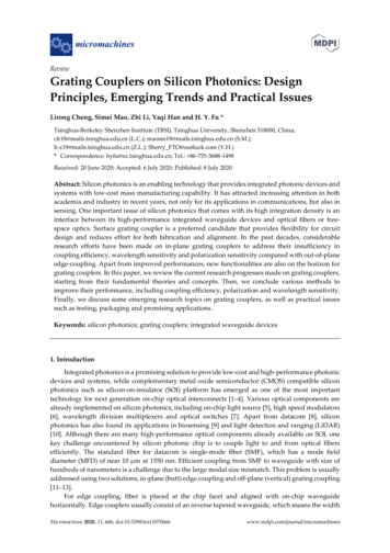
RAHIM et al.: OPEN-ACCESS SILICON PHOTONICS PLATFORMS IN EUROPE8200818A. Imec’s Silicon Photonics Platformimec, in collaboration with Ghent University, was among thefirst to demonstrate the power of DUV lithography for siliconphotonic ICs [3]. imec’s ISIPP50G technology is based on a130 nm CMOS node toolset. It uses SOI wafers with 220 nmthick guiding silicon layer with 2 μm BOX in its 200 mm R&Dpilot line. The technology includes 193 nm lithography for highfidelity patterning of a variety of passive devices possible dueto the provision of three etch levels (one full and two partialetch levels). The technology uses optimized Inductively CoupledPlasma - Reactive Ion Etching (ICP-RIE) dry etch processes. Itoffers a poly-silicon overlay layer for high-efficiency couplingto and from SOI chips. To achieve active functionalities, such as(high-speed) modulation, ISIPP50G platform offers four levelsof P-type and N-type doping each. Photodetection is enabledby a low-defect epitaxially grown Germanium on silicon. Thetechnology provides various features at the Back-End-Of-Line(BEOL) such as local removal of the dielectric stack for improving the coupling efficiency of the grating couplers and access tothe Front-End-Of-Line (FEOL) and a deep etch through the fullstack into the silicon substrate for fiber edge coupling.imec’s ISIPP50G technology finds a wide range of applications ranging from optical communication, sensing to spectroscopy. The technology has a high TRL of 7. The accessto the technology is possible via MPW service provided byEuropractice IC (http://www.europractice-ic.com/), which offers at least three MPW runs in a year. Moreover, imec alsoprovides dedicated engineering runs as well as low-volumemanufacturing.The components library of imec includes a wide variety ofpassive and active devices for O- and C-band applications.The three etch levels support strip waveguides (typical loss of1.6 dB/cm for C-band) and rib waveguides (for C-band, typical loss of 1.1 dB/cm and 0.7 dB/cm for deep and shallowetched waveguides, respectively). A variety of grating couplers(1D, curved and high-efficiency grating couplers) are part ofthe component library. It also includes low-loss and broadbandedge couplers. For splitting and combing of light, the libraryincludes directional couplers and MMI couplers (1 2 and 2 2) with a negligible power imbalance, good phase accuracy andsmall excess loss over the C-band. The key feature of imec’s silicon photonics technology is the availability of 50G modulatorsand detectors for datacom/telecom applications operating in Oand C-band. The components library provides carrier depletionbased lateral PN junction Mach-Zehnder modulator (MZM) andring modulator with an integrated thermal heater to tune the operating wavelength of the modulator. Recently, a compact Germanium Electro-Absorption Modulator (EAM) using the FranzKeldysh effect is included in the component library. It providesup to 100 Gb/s modulation speed. The technology offers lowdark current photodiodes with either high responsivity or highbandwidth to support up to 100 Gb/s data rates [10], [33]. Anoverview of the components offered by imec’s ISIPP50G tecnology is shown in Fig. 1.The capability to imec’s ISIPP50G platform is illustratedby an ultra-dense 16 56 Gb/s NRZ transceiver. It uses aFig. 1. imec’s fully integrated silicon photonics platform for 1310 nm/1550 nmwavelengths comprising low-loss passive waveguide devices, efficient fiber I/Oand 50 Gb/s modulators and detectors.multicore fiber to implement a short-reach optical link with atransmission capacity of 896 Gb/s. The transceiver has a formfactor of 1.47 mm2 highlighting the dense photonic integration using silicon photonics technology. The transceiver usesthe GeSi waveguide electro-absorption device as a modulatorand a photodetector. The 16-channels of the demonstrator aredriven at 56 Gb/s and are tested sequentially. An open eye diagram with an SNR of 3.05 to 3.92 dB has been recorded at1565 nm (L-band) when driven with 2.5 Vp p RF signal and 2.5 V reverse bias for the photodiode [34].The Process Design Kit (PDK) is available via various EDAsoftware vendors. The PDK contains the static GDS files, maturity levels and variability statistics of the library components.The PDK aids the designers for custom component designs byproviding details of the technology, typical process tolerances,layer specifications and design rules. The future versions of thePDK will contain Layout vs. Schematic (LVS) verification to reduce design errors and Lithography Friendly Design (LFD) toimprove the patterning predictability.For the future, imec is developing efficient thermo-optic phaseshifting elements by substrate undercutting. Such heaters canreduce the power consumption by a factor of 4. Furthermore,imec is developing technology to improve the performance ofpassive waveguide circuits through the integration of SiN in itstechnology platform.To address the long-term market needs, imec, in collaboration with Ghent University, is actively engaged in developingtechnologies for low-cost integration of laser sources on itssilicon photonics platform. As an example, transfer printingis developed for simultaneous transfer of multiple (semi-)processed III-V lasers from the source III-V wafer to thetarget silicon photonics wafer [35]. The technology promisesmassive richness of functionality and performance and allowsfor efficient use of III-V material.B. CEA-Leti’s Laser-Integration Compatible SiliconPhotonics PlatformLeti has developed a fabrication platform for siliconphotonics-based circuits allowing large-scale integration of active and passive devices in a flexible CMOS compatible process.This platform provides more than silicon with the integration of
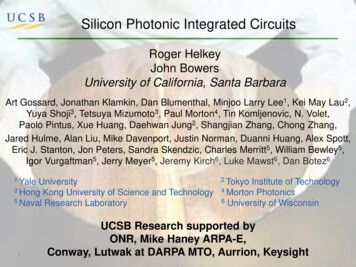
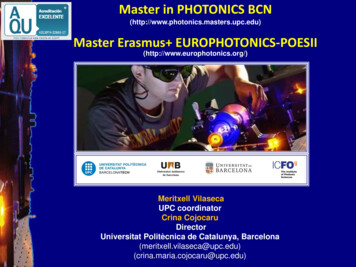
8200818IEEE JOURNAL OF SELECTED TOPICS IN QUANTUM ELECTRONICS, VOL. 25, NO. 5, SEPTEMBER/OCTOBER 2019Fig. 3. Cross-section of IHP’s EPIC technology platform (image of the firstgeneration EPIC technology with 30 GHz photo detector). Locally reconstructedbulk Silicon by using epi CMP enables frontend-of-line integration approachof SiGe electronics with state-of-the-art SOI-based photonics.Fig. 2. CEA-Leti’s silicon photonics platform: (a) Cross section of the overallplatform. (b) III-V die bonded on patterned silicon.a SiN layer and is compatible with III-V bonded epilayer on thesame wafer, offering the advantages of each material. This convergence of different photonic platforms in this multi-materialsprocess allows addressing various application needs with in thesame platform.The silicon core process is based on an SOI wafer with asilicon film thickness of 305 nm. This thickness enables improved performance of passive devices as compared to the former 220 nm technology [36]. A modular approach is used tobuild the process flow that supports various sets of devices.Multi-level silicon patterning module allows the fabrication ofwaveguide with different slab heights, leading to different optical characteristics, which can be mixed inside the same die. ADUV 193 nm lithography mask level defines the most criticalpatterns. Up to eight levels of implantation are available in orderto define the various type of lateral PN-based phase modulators.Modulation of up to 64 Gb/s has been demonstrated with thiscore silicon process [37]. Selective Germanium epitaxy is usedto form the absorbing section of the device. The integrated photodiode is based on a SiGeSi architecture leading to a better lightconfinement compared to a full-Ge device [38]. A second optical layer made of SiN is integrated on top of the silicon. Thislayer can be used to design specific SiN-based devices or hybridSiN/Si devices [39]. A two metal level BEOL is available withan integrated heater for thermal wavelength tuning of devices.Figure 2(a) presents the cross section of the overall platform.InP-based epitaxial layer can be integrated on top of the silicon layer of LETI’s platform. Wafer or die bonding is availabledepending on the level of integration needed. Post-bonding fabrication is performed without downsizing the initial SOI waferand using “CMOS-friendly” processes and materials allowingthe large-scale integration of III-V based device on the maturesilicon photonic platform (see Fig. 2 (b)).The PDK supporting this platform proposes two device libraries containing a large set of devices to address O-band andC-band applications. The technology is accessible through thebroker CMP (https://mycmp.fr/) with two MPW runs/year (without III-V integration) and has a TRL of 7.The current focus of developments is on optimized hybridlaser designs taking into account the new capabilities offered bythe CMOS compatible processes. Technology transfer to LETI’s300 mm fabrication line is ongoing. Advanced EIC/PIC integration solutions based on 50 μm pitch micro-bumps are availablefor dedicated customers and projects. Furthermore, TSV integration on silicon photonic platform is under development. Theoverall platform is becoming versatile enough to address morethan telecom/datacom applications. Application diversificationis a crucial issue for the sustainability of the silicon photonics.New markets such as advanced computing, 3D sensing or cryptography can be targeted with LETI’s silicon photonics platform.C. IHP’s Monolithic Electronic-Photonic PlatformThe goal of IHP’s monolithic electronic-photonic integrationplatform is to deliver the integration of the basic componentsof electro-optic transceiver (i-e, modulator, driver, amplifier,photo-detector,.) on a single chip, which has SiGe HeteroJunction Bipolar Transistors (HBTs) and PICs. IHP uses200 mm SOI wafers with 220 nm guiding layer thickness on2 μm BOX for a platform providing monolithic ElectronicPhotonic Integrated Circuits (EPICs). The platform uses DUV(KrF) and i-line 250 nm CMOS-baseline technology. The technology has a mixed electronic-photonic frontend with fivemetal layers at the backend (three thin and two thick) and cointegration with high-performance HBTs as shown in Fig. 3.The technology is developed for C- and O-band applicationsand has a TRL of 7. IHP’s high performance BiCMOS technology SG25H5-ePIC is available to academic and industrialusers in MPW mode through Europractice IC. IHP also provides
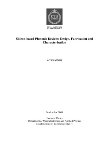
RAHIM et al.: OPEN-ACCESS SILICON PHOTONICS PLATFORMS IN EUROPEdirect access to its technology through dedicated engineeringruns. Key building blocks in IHP’s EPIC technology are:(i) nano-waveguides (etch depth 220 nm, 120 nm, 70 nm)with loss between 1-3.5 dB/cm, (ii) Standard Single Mode Fiber(SSMF) compatible 1D grating couplers with a typical insertionloss of 4.5 dB, (iii) MMI based splitters/combiners (1 2, 2 2, 4 4), (iv) Carrier dispersion based phase shifters (lateralPN, lateral PIN), (v) linear lateral PN with Vπ L 2.8 V.cm and1.2 dB/mm @-1 V, (vi) thermal phase shifters, (vii) Waveguidecoupled Germanium PIN detectors with responsivity 0.9 A/W(internal), OE-S21 3dB 60 GHz, dark current 200 nA @ roomtemperature, 2 V, (viii) HBTs with BVCEO 1.65 V, fT 220 GHz and fmax 290 GHz [12], [40], [41]. Figure 3 showsthe cross section of IHP’s EPIC technology.Recently, IHP’s technology has been used to demonstrate anovel Mach-Zehnder modulator that is monolithically integratedwith drivers in a photonic BiCMOS technology. The MZM consists of two 6 mm long parallel phase shifting elements. Theyare divided into 16 segments that are based on waveguide diodesand utilize the carrier dispersion effect to induce phase changes.The overall Vπ of the modulator is 3.9 V at 1 V reverse biasand a fiber-to-fiber optical loss of 18 dB. The modulator driveris monolithically integrated with the modulator. The combinedelectro-optical S21 spectrum of the driver and modulator exhibitsa slow roll-off with 3 dB and 6 dB bandwidth of 11 GHz and36 GHz, respectively. The monolithically integrated modulatorwith a driver is used to demonstrate data transmission of net300 Gb/s over 120 km SSMF. [42].The PDK of the technology is developed for Cadence as wellas TexEDA with fully featured electronic PDK, fundamentaloptical cells, electronic-photonic Design Rule Check (DRC),photonics-enabled LVS and script-based filler generation. Moreover, the PDK provides parametric building blocks and opticalcircuit simulation (optical S-Parameter transient) using IPKISS. The upcoming features of the technology include higherperformance HBT module integration, low-loss edge couplingand on-chip polarization management. In the long-term, IHP isstriving to provide an integrated laser source on its EPIC platform. Regarding hybrid integration of other platforms, IHP collaborates with commercial partners. Solder bumping and copperpillars are available with 120 μm and 70 μm pitch, respectively.As for the photonic-electronic integration roadmap, IHP plansto provide co-integration with HBT performance of ft /fmax of300/500 GHz in the mid-term future.D. VTT’s Thick-SOI PlatformThe foundation for VTT’s Thick-SOI technology platform isthe Micronova clean room facility where the first silicon photonics components were designed in 1997, and fabricated a fewyears later. Today, the main technology platform is based on3 μm thick SOI where light is almost fully confined inside the Sicore. The combination [43] of single-mode rib waveguides andmulti-mode strip waveguides offers a unique combination of lowlosses ( 0.1 dB/cm), dense integration (bend radii 1–30 μm) andsmall polarization dependence in effectively single-mode PICs.In addition to fully passive components, also thermo-optic phase8200818Fig. 4. (a) Top view of a 35 cm long waveguide spiral. (b) Simulation ofthe fundamental mode for the 3 µm 1.875 µm silicon strip waveguide.(c) Rib-to-strip converter for coupling to the fundamental mode [47].modulators, plasma dispersion modulators and Ge photodiodeshave been developed. Compared to the performance of similar devices in sub-micron SOI, the performance of passive andthermo-optic components is often better, while the bandwidthof high-speed active components is much lower (well below10 GHz).Silicon photonics has become the most important driver forVTT to develop the Micronova clean room facility. 3 μm SOIforms the basis for silicon photonics research and related smallvolume manufacturing in Micronova. Continuous platformdevelopment covers TRL range 1–9. There is additional development on 12 μm SOI for optical interposers between SSMFarrays and PIC chips.VTT offers up to two MPW runs/year in 3 μm SOI. Dedicatedruns and other R&D services from design and process development to hybrid integration, packaging and chip/wafer level testing are carried out for customers around the world. They rangefrom small university groups to large-scale companies. Contractmanufacturing in Micronova is offered by VTT Memsfab, a separate company within the VTT group. Also, technology transferand IP licensing are available. VTT provides direct access to itstechnology platform (www.vtt.fi/siliconphotonics).The key building blocks in MPW technology are single-moderib waveguides ( 0.1 dB/cm), multi-mode strip waveguides( 0.15 dB/cm including bends), rib-strip converters ( 0.05 dB)[43], Euler bends ( 0.01 dB for 20 μm radius) [44], TIR mirrors (0.1–0.3 dB), thermo-optic phase modulators ( 0.01 dB, 10 kHz, 25 mW/π), PIN modulators ( 1 MHz, 5 mW/π),MMI couplers (0.1–0.2 dB), Mach-Zehnder interferometers,echelle gratings (1–4 dB), Arrayed Waveguide Gratings (AWGs)(2–5 dB) and dry-etched I/O facets with anti-reflection coatings( 0.5 dB coupling loss to lensed fibers). Dedicated runs alsoinclude up-reflecting mirrors with either 55 or 45 mirror angle(0.5–2 dB) and Ge photodiodes ( 10 GHz). Hybrid integrationmounts (with end-fire coupling) can be fabricated for variousoptoelectronic chips that are obtained either from the customeror from other service providers.One key capability of the thick-SOI platform is to realizelong and low-loss waveguide spirals in ultra-small footprint (seeFig. 4). They can be used to measure precisely the propagationloss of the waveguides and they have been used, for example,
8200818IEEE JOURNAL OF SELECTED TOPICS IN QUANTUM ELECTRONICS, VOL. 25, NO. 5, SEPTEMBER/OCTOBER 2019to demonstrate demodulators for phase-shift-keying [45], Faraday rotation [46] and Instantaneous Frequency Measurement(IFM). In particular, IFM has been demonstrated in collaboration with the University of Sydney and the results were reported in [47]. The 35 cm long waveguide spiral used in thisdemonstration is shown in Fig. 4 and it allowed to efficientlyharness Kerr non-linearity and to demonstrate the first on-chipfour-wave mixing-based IFM
oping open-access silicon photonics technologies [21]. In cer-tain cases, the CMOS pilot lines and research institutes partner with pure-play CMOS fabs for the seamless translation from prototyping towards high-volume manufacturing [22]. While originally silicon photonics was synonymous for PIC-platforms based on Silicon-on-Insulator (SOI .
