Transcription
MENU !(/)SYSTEM-LEVEL DESIGN (/CATEGORY-MAIN-PAGE-SLD/)Silicon Photonics Comes Into Focus2114923Using light to move large quantities of data looks promising, but gaps remainand the adoption timeline will vary by application.OCTOBER 31ST, 2016 - BY: ED NG/)Silicon photonics is attracting growing attention and investment as a companiontechnology to copper wiring inside of data centers, raising new questions about whatcomes next and when.Light has always been the ultimate standard for speed. It requires less energy to movelarge quantities of data, generates less heat than electricity, and it can work equallywell over long or short distances. Moreover, many experts contend it will be harder tohack data delivered with photons than over a copper wire.For all of these reasons and others, investments are increasing in silicon photonics(http://semiengineering.com/kc/knowledge center.php?kcid 41). A study by UCSanta Barbara showed that between 2009 and 2015, the number of papers more thandoubled to roughly 14,000. In 2005, there were about 500 papers on the subject.
Unlike in the past, when most research was funded academic or government sources,today’s funding is largely from commercial s-ups-and-downs/).There are signs of tangible progress on other fronts, as well. Mentor eid 22017) and id 22032) have tool flows for siliconphotonics design. Synopsys (http://semiengineering.com/kc/entity.php?eid 22035), meanwhile, has been expanding its photonics and simulation software linethat it acquired when it bought RSoft Design Group in 2012. And GlobalFoundries hasramped up its investment in the process for commercializing it. Now the question ishow quickly the infrastructure can be developed, vetted, and ramped to utilize siliconphotonics for new applications and in new markets.The long-term goal is to use photons to carry data across a chip, eventually replacingSerDes, traditional interconnects and maybe even conventional transistors. But thatcould take a decade or more. The short- and mid-term goals are more focused on thedata center and within the network, where data is ballooning from video, various typesof imaging (including embedded vision and virtual/augmented reality), and aproliferation of sensors with the Internet of Things. The first mass deployment of lightbased communication began in the 1990s, using fiber optics to lay the backbone forthe Internet. It has since expanded into data centers, where silicon photonics is used tocommunicate between racks of servers, and between those servers and storage. Thenext phase is expected to involve communications between chips within a package.But there are a number of technical and business-related challenges that must beresolved to really propel this technology forward. Light sources based on materialssuch as gallium arsenide, indium arsenide (InAs) or indium gallium arsenide (InGaAs)need to be more tightly coupled into the manufacturing process to achieve economiesof scale, which has been problematic in the past because these III-V materials aredifficult to work with using conventional silicon processes.In addition, tools are required to effectively deal with waveguide sidewall roughness,spatial separation, and die-level variation in waveguides and devices, according to JohnBower, a UC Santa Barbara professor and deputy CEO of the American Institute for
Manufacturing of Photonics (AIM), a joint effort between the U.S. government anduniversities in New York, Massachusetts and California.“What’s needed now is to increase the lifetime of these lasers,” said Bower. “The goal is4,000 hours. We’ve seen 2,100 hours, which is not sufficient for anyone’s laser.”How rapidly those changes will be implemented isn’t clear. Nevertheless, estimates ofthe size of this market are enough to warrant at least some attention.GlobalFoundries (http://semiengineering.com/kc/entity.php?eid 22819) expectsthis will become a 3 billion market within three years, facilitated by continuedimprovements in process technology to more easily incorporate light sources intosilicon, which has been the chief problem identified by proponents of the technology.And given the data growth rates, silicon photonics is on a very short list of possiblesolutions.“IP (Internet protocol) traffic is overwhelming bandwidth,” said Ted Letavic, seniorfellow at GlobalFoundries. “Mobile data use will be 30.6 exabytes per month by 2020.”Letavic believes the first major impact of silicon photonics will be the re-architecting ofthe data center. Rather than one or two huge data centers, he said the current thinkingis to set up many smaller data centers and connect them with silicon photonics.“Optical interconnects will replace copper and be used to augment microwave andmillimeter wave. And with 5G, you will need a high-speed interconnect from the datacenter to small cells. You will need at least 1 gigabit per second to the edge node, and16 to 25 gigabits per second between the small cell and the base station.”That scale-out will involve heterogeneous networks, or HetNets(http://semiengineering.com/kc/knowledge center.php?kcid 232), and these willbenefit from photonics integration, he said. Then, over time, this technology willmigrate into 2.5D, 3D and monolithic packages. “Thermal-optical effects still have to bevery accurately models, and substantial improvement is needed on waveguide design.We also need more structured toolsets for reliability.”
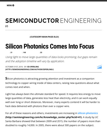
GlobalFoundries isn’t alone in seeing silicon photonics as a big opportunity. HewlettPackard Enterprise, Intel and Juniper Networks, all are aggressively pursuingheterogeneous integration of photonics, said UCSB’s Bower. Cisco has a big investmentin this market, as well.Silicon photonics, in a nutshell, relies on optical waveguides rather than copper toroute the light. The real challenge is incorporating the light source into silicon as part ofthe manufacturing process. The current approach uses quantum wells—basicallycreating a sandwich of one III-V material, such as gallium arsenide, between layers of aanother III-V material, such as indium gallium arsenide. By doing that the electrons aretrapped perpendicular to the layer surface, to create a laser light source.Research is underway to replace quantum wells with quantum dots, which can befinely tuned by changing the size or shape of the dot. As current is applied, the dotsemit light at very specific frequencies. Researchers say this will reduce the cost forintegrated light sources, lower the power threshold, and increase reliability over s/2016/10/004730 10 fig1.jpg)Hybrid silicon III-V optical amplifier. Quantum wells are in red. Source: SPIE
ptation vs. reinventionDespite some fundamental differences in the technology between photonics andsilicon-based semiconductors, there also are some overlaps.“Thirty mask layers are common, and there are more than 400 elements per chip,” saidBower. “What we need is a photonics version of Moore’s Law.”There are other similarities, as well. “The most sensitive parameters like line width andedge roughness are already being dealt with in silicon,” said Duane Boning, professorof electrical and computer science at MIT. “Sensitivity lags IC applications, but withGlobalFoundries moving from 200mm to 300mm processes, there will be bigimprovements in photonics. You get finer process control. CMOS technology is still acouple generations ahead, but what we’re seeing in photonics is that it’s gatheringenough replication to understand more subtle variations. So we understand thicknessof wafers, for example. And we’ve had to deal with so much variation around thermalthat we have had to adapt and tune structures.”He said that some of these approaches may be hard to translate to the siliconphotonics world, but they don’t have to be reinvented.Techniques on the design side are applicable, too. “There is a lot of stuff we learned atadvanced nodes, like self-heating, where the solution is very applicable to photonicsbecause it provides a thermal map,” said Gilles Lamant, distinguished engineer atCadence. “We also have dealt with line-edge roughness on fins, which is very applicableto waveguides. There is a potential to provide other things to photonics, as well, suchas design for manufacturing.”Added Lamant: “The key is making sure that design intent is correctly implemented.”Process design kits are in the works for silicon photonics, as well. Chris Cone, productmarketing manager for Pyxis IC Station at Mentor Graphics, said that to create a designwith photonics you take a PDK and build it around two or three specialized devices.
“Photonics is a new market, so basically you’re designing around a novel device. Butyou’re still doing verification for DRC (design rule checking) and LVS (layout versusschematic), lithography simulation, and you still need a full flow as you do in CMOS.”PhoeniX Software, based in the Netherlands began developing PDKs in 2008 with Imecfor silicon photonics, according to Twan Korthorst, PhoeniX’s CEO.Korthorst noted that other areas are being explored, as well, including biophotonics,where sensing is done with light rather than electronics. “Some light is not confined tothe waveguide. It’s influenced by a surrounding ring, which you coat with a chemical.So that chemical may be sensitive to certain bacteria. We’re seeing commercialcompanies working with this in the biological domain.”Mentor’s Cone pointed to another biomedical application involving sensors createdfrom an array of micro-capillaries. “You’re able to sort out molecules based upon themolecule source. Then you use optics to interact with them and find potentialpathogens in the blood.”Progress on other fronts, tooWhile silicon photonics may provide a huge reduction in latency, it’s not the only pieceof the puzzle. For data to move at the speed of light, everything else has to be speededup, as well. That means signals need to be processed and routed much faster thantoday. At the chip level, this ultimately could become a requirement because of the RCdelay in increasingly skinny wires, thinner contacts, and a predicted breakdown indielectrics at the most advanced nodes.“There is always a need for higher and higher communication speeds,” said MikeGianfagna, vice president of marketing at eid 22242). “We’ve seen that withSerDes in the high-end network and compute space. We’ve also seen that in theinterface between high-bandwidth memory and the mission-critical stack. Demand forhigher-bandwidth is holding steady, which right now makes SerDes the most criticalelement. It’s like the price of admission these days. It’s been shown to have reliabledeployment.”
How long that will be good enough, and when SerDes will run out of steam andprovide an opportunity for photonics, is unknown.“In the networking space there has been talk about high-bandwidth, low-latencytechnology that would replace SerDes,” said Kurt Shuler, vice president of marketing atArteris (http://semiengineering.com/kc/entity.php?eid 22674). “For some chips insome niches, photonics may work, and maybe in the future we’ll see it chip-to-chip.We’ve been working with the CCIX (Cache Coherent Interconnect for Accelerators)Consortium, where everything will run on a PCIe PHY using a CCIX controller. In thefuture, that won’t be on a board. But you will still need physical connectivity, andphotons produce less heat.”Shuler said that at the chip level, the big bottleneck is communication between the SoCand DRAM. “If you look at high-bandwidth memory (HBM) and the Hybrid MemoryCube, everyone is trying to work around that. But DRAM is still slower and cheaper, sogiven that constraint, how do you make everything run faster? One solution is to addmore SRAM. You can build in cache coherency and proxy caches, and it helps if anyelement can use it rather than just one processor. But with DRAM, it’s not just aboutlatency and bandwidth. It’s also about power.”And this is where photonics really excels. “If you take a look at the trends on the roadmap, there is a move to get away from silicon,” said Greg Yeric, an ARM(http://semiengineering.com/kc/entity.php?eid 22186) fellow. “That includesmaterials such as germanium and indium-gallium-arsenide. It’s inconceivable thatphotonics won’t be part of that, and someday you’re going to see a dedicatedphotonics chip in a package for the people who really care about performance. We alsomay see a move toward plasmonics. With nanometer manufacturing capability, youcan make the right thickness and pattern of film and convert from a photon to aplasmon.”But how quickly all of this technology gets rolled up into a vibrant market opportunitymay depend on how well other technologies fare. A classic comparison is in the area ofEthernet, which everyone assumed would die off when wireless became pervasive.Quite the opposite occurred.
“Industrial is all moving to Ethernet because of economies of scale,” said Lixin Zhou,senior director of the switching product line at id 22903). “If you look at highperformance computing, the majority of those are based on Ethernet now. It used tobe InfiniBand and Fibre Channel. Now it’s Fibre Channel over Ethernet.”When Ethernet was introduced back in 1980, it had a transfer rate of 2.94Mbits/second. The latest Ethernet speeds run as high as 100 Gbits/second, andEthernet speeds inside of existing transceivers are increasing from 25 Gbps/line to 10Gbps/cable for a four-cable connection, which also provides more granularity incontrolling traffic.Whether that will be enough to offset adoption of faster technologies such asphotonics may depend on the application, but the point is that nothing is standing still.So while photonics is definitely on the horizon, the timing needs to be considered inthe context of other technologies, the challenges of sticking with Moore’s Law, and avariety of other issues that are only tangentially connected to photonics.ConclusionsThe promise of photonics is enormous. It’s not clear whether speed will be the maindriving force, or whether power and thermal effects will propel it forward. It may beone or all of them. But it’s not clear when this will happen or for which markets it willhappen first.This is a technology that is still in its infancy, and change is swirling around almostevery aspect of the electronics design through manufacturing flow. Quantumcomputing (http://semiengineering.com/kc/knowledge center.php?kcid 207),neural networks, artificial intelligence and machine learning(http://semiengineering.com/kc/knowledge center.php?kcid 305) all will have animpact on the volume and required speed of moving data, and photonics will be apiece of the puzzle. How big of a market it garners, where that happens—whether itremains as a communications channel between racks of servers and storage orwhether it moves further to the chip—and when are all big question marks.
Nevertheless, nothing moves faster than the speed of light, and with the amount ofmoney pouring into research, this market appears to be moving rather quickly.Related StoriesPhotonics Moves Closer To Chi to-chip/)pGovernment, private funding ramps up as semiconductor industry looks for faster low-powersolutions.Focus Shifting To Photonics onics/)Using light to move data will save power and improve performance; laser built into processtechnology overcomes huge hurdle.21TAGS:149232.5D (HTTP://SEMIENGINEERING.COM/TAG/2-5D/)AMERICAN INSTITUTE OF MANUFACTURING OF PHOTONICS -OFMANUFACTURING-OF-PHOTONICS/)ARM (HTTP://SEMIENGINEERING.COM/TAG/ARM/)ARTERIS (HTTP://SEMIENGINEERING.COM/TAG/ARTERIS/)CADENCE (HTTP://SEMIENGINEERING.COM/TAG/CADENCE/)CISCO (HTTP://SEMIENGINEERING.COM/TAG/CISCO/)ESILICON (HTTP://SEMIENGINEERING.COM/TAG/ESILICON/)GALLIUM ARSENIDE GLOBALFOUNDRIES ETNETS (HTTP://SEMIENGINEERING.COM/TAG/HETNETS/)HEWLETT PACKARD ENTERPRISE TERPRISE/)IMEC (HTTP://SEMIENGINEERING.COM/TAG/IMEC/)INDIUM ARSENIDE NDIUM-GALLIUM-ARSENIDE ENIDE/)INTEL (HTTP://SEMIENGINEERING.COM/TAG/INTEL/)JUNIPER NETWORKS LOW POWER (HTTP://SEMIENGINEERING.COM/TAG/LOW-POWER/)MARVELL (HTTP://SEMIENGINEERING.COM/TAG/MARVELL/)MENTOR GRAPHICS IT (HTTP://SEMIENGINEERING.COM/TAG/MIT/)PHOENIX SOFTWARE PLASMONICS (HTTP://SEMIENGINEERING.COM/TAG/PLASMONICS/)SERDES (HTTP://SEMIENGINEERING.COM/TAG/SERDES/)UC SANTA BARBARA WAVEGUIDES (HTTP://SEMIENGINEERING.COM/TAG/WAVEGUIDES/)Ed Sperling(all posts) (http://semiengineering.com/author/esperling/)Ed Sperling is the editor in chief of Semiconductor Engineering.
2.org)NEWSLETTER SIGNUPEmail:
Interests:System-Level DesignLow Power-High PerformanceManufacturing, Design & TestIoT, Security & AutomotiveSubscribe(/)ABOUTAbout us (http://semiengineering.com/corp)Contact us (http://semiengineering.com/corp)Advertising on SemiEng mepage (http://semiengineering.com/)System-Level Design /)Low Power-High Perf p/)Manufacturing Des & Test ufacturing-design/)IoT, Security & Automotive -security/)Knowledge Centers (http://semiengineering.com/kc)Startup Corner (http://semiengineering.com/startup-corner)Bus & Marketing Strategies rategies/)CONNECT WITH USFacebook (https://www.facebook.com/SemiEngineering)Twitter (http://www.twitter.com/SemiEngineering) @semiEngineeringLinkedIn ineering)YouTube pyright 2013-2016 SMG Terms of Service (http://semiengineering.com/terms-of-service/) Privacy Policy(http://semiengineering.com/privacy/)
Added Lamant: "The key is making sure that design intent is correctly implemented." Process design kits are in the works for silicon photonics, as well. Chris Cone, product marketing manager for Pyxis IC Station at Mentor Graphics, said that to create a design with photonics you take a PDK and build it around two or three specialized devices.