Transcription
ReviewGrating Couplers on Silicon Photonics: DesignPrinciples, Emerging Trends and Practical IssuesLirong Cheng, Simei Mao, Zhi Li, Yaqi Han and H. Y. Fu *Tsinghua-Berkeley Shenzhen Institute (TBSI), Tsinghua University, Shenzhen 518000, China;clr18@mails.tsinghua.edu.cn (L.C.); maosm19@mails.tsinghua.edu.cn (S.M.);li-z19@mails.tsinghua.edu.cn (Z.L.); Sherry FTO@outlook.com (Y.H.)* Correspondence: hyfu@sz.tsinghua.edu.cn; Tel.: 86-755-3688-1498Received: 20 June 2020; Accepted: 6 July 2020; Published: 8 July 2020Abstract: Silicon photonics is an enabling technology that provides integrated photonic devices andsystems with low-cost mass manufacturing capability. It has attracted increasing attention in bothacademia and industry in recent years, not only for its applications in communications, but also insensing. One important issue of silicon photonics that comes with its high integration density is aninterface between its high-performance integrated waveguide devices and optical fibers or freespace optics. Surface grating coupler is a preferred candidate that provides flexibility for circuitdesign and reduces effort for both fabrication and alignment. In the past decades, considerableresearch efforts have been made on in-plane grating couplers to address their insufficiency incoupling efficiency, wavelength sensitivity and polarization sensitivity compared with out-of-planeedge-coupling. Apart from improved performances, new functionalities are also on the horizon forgrating couplers. In this paper, we review the current research progresses made on grating couplers,starting from their fundamental theories and concepts. Then, we conclude various methods toimprove their performance, including coupling efficiency, polarization and wavelength sensitivity.Finally, we discuss some emerging research topics on grating couplers, as well as practical issuessuch as testing, packaging and promising applications.Keywords: silicon photonics; grating couplers; integrated waveguide devices1. IntroductionIntegrated photonics is a promising solution to provide low-cost and high-performance photonicdevices and systems, while complementary metal oxide semiconductor (CMOS) compatible siliconphotonics such as silicon-on-insulator (SOI) platform has emerged as one of the most importanttechnology for next generation on-chip optical interconnects [1–4]. Various optical components arealready implemented on silicon photonics, including on-chip light source [5], high speed modulators[6], wavelength division multiplexers and optical switches [7]. Apart from datacom [8], siliconphotonics has also found its applications in biosensing [9] and light detection and ranging (LiDAR)[10]. Although there are many high-performance optical components already available on SOI, onekey challenge encountered by silicon photonic chip is to couple light to and from optical fibersefficiently. The standard fiber for datacom is single-mode fiber (SMF), which has a mode fielddiameter (MFD) of near 10 μm at 1550 nm. Efficient coupling from SMF to waveguide with size ofhundreds of nanometers is a challenge due to the large modal size mismatch. This problem is usuallyaddressed using two solutions, in-plane (butt) edge coupling and off-plane (vertical) grating coupling[11–13].For edge coupling, fiber is placed at the chip facet and aligned with on-chip waveguidehorizontally. Edge couplers usually consist of an inverse tapered waveguide, which means the widthMicromachines 2020, 11, 666; chines
Micromachines 2020, 11, 6662 of 25of waveguide is gradually decreasing along the propagation of light to the edge [14]. As it graduallydecreases, light confinement is reduced and the mode size becomes larger to be comparable withfiber mode. It is reversed for fiber-to-chip propagation case, where Gaussian fiber mode distributionwill be confined in the tapered waveguide as its size gradually increase. Edge couplers can achievehigh coupling efficiency (CE), large bandwidth (BW) and low polarization dependent loss (PDL) [11].However, a properly cleaved and polished facet with strict smoothness requirement is needed toreduce the loss, which adds extra fabrication cost considering mass manufacturing. The highperformance also comes with reduced flexibility, since they have relatively large footprint and mustbe placed at the edge of chip. In addition, edge coupling solutions have low fiber-chip alignmenttolerance and prohibit wafer-level testing, which will further increase the cost per chip and requirehigher accuracy for testing and packaging.On the contrary, vertical grating couplers (GCs) are much more flexible in terms of arbitrarycoupling position on chip, compact size, easy fabrication and wafer-level testing capability. Forgrating coupling, fiber is placed above diffractive grating structures on the top of chip. A vertical GCchanges the off-plane wave-vector direction of light to the in-plane waveguide direction, and thencouples the light into waveguide using a spot-size converter. Although GCs have the abovementioned advantages, they also have some drawbacks coming with their operation principles. First,they usually have lower CE compared with edge couplers, while numerous research works havefocused on improving CE of GC. Secondly, gratings are intrinsically sensitive to both wavelength andpolarization. We first introduce basic working principles and theories for GCs, and then we reviewspecific design principles that are widely adopted to overcome these limitations. In addition, we alsodiscuss some emerging research trends in silicon PIC that also apply to GC design, including newfunctionalities, new design methodology and new material platforms in recent years. Finally,practical issues concerning testing, packaging and applications of GC are also provided.2. Fundamentals of Grating CouplerGrating is basically a varying arrangement of different materials or structures on certain surface,usually periodic. On SOI-based photonic chips, it is realized through etching on SOI or selectivelydepositing amorphous silicon on SOI. Either etching or deposition creates refractive index variation.If the index variation has a period larger than the wavelength of light inside the grating material,diffraction effect prevails. Otherwise, the light propagation in grating will exhibit similar feature asuniform medium, which becomes more significant as its period decreases [15–17]. GCs, as depictedin Figure 1, work in the diffraction regime. For a surface GC, if the refractive index varies only in onedirection, we call it a 1D-GC and light is coupled in the direction of index variation. For simplicity,we analyze the diffraction GC working principles in terms of 1D-GC, while the theories are also validfor 2D-GC if only the propagation direction works in a diffraction regime. However, if both directionswork in diffraction regime, light can propagate in both directions and the 1D-GC working principlesapply for both directions. For a GC with straight gratings, a spot-size converter based on taperedwaveguide of hundreds of microns is required to convert the coupled fiber mode into a 500-nmwaveguide mode, while a confocal grating allows compact design of GC with tens of microns infootprint.
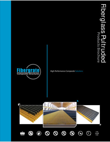
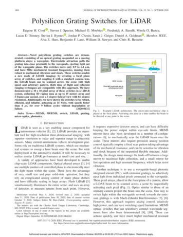
Micromachines 2020, 11, 6663 of 25Figure 1. Schematic structure for a 1D grating coupler (GC) with linear waveguide taper and keyparameters: periodΛ , fiber tilt angle θ, varying taper width W and taper angle θ taper .2.1. Bragg Condition, Loss Channels and Fiber Tilt AngleThe diffraction behavior for a GC, as illustrated in Figure 2a, can be described using Braggcondition (also called phase matching condition), which reveals the relationship between wavevector k0 of an incident light beam above chip and propagation constant β of the correspondingcoupled light beam into the waveguide. The Bragg condition is expressed ask0 sin mG βm ,(1)where G is the grating vector and m is the grating diffraction order. This equation is better depictedby a wave-vector diagram, as shown in Figure 2b for fiber-to-chip coupling, while a similar analysisalso applies for chip-to-fiber case.(a)(b)(c)Figure 2. (a) Loss channels in input and output coupling; (b) wave-vector diagram for fiber-to-chipcoupling; and (c) wave-vector diagram for chip-to-fiber perfectly vertical coupling.The Bragg condition only predicts which diffraction order is allowed, instead of energydistribution between different orders or diffraction efficiency. CE is usually obtained using a
Micromachines 2020, 11, 6664 of 25numerical method such as finite element time domain (FDTD) calculations [18]. To estimate the CEqualitatively, we can analyze some major power loss channels, as marked in Figure 2a. Firstly, for theinput coupling case on the left side of Figure 2a, some uncoupled power will propagate downwards.Although part of that power can be reflected if the oxide thickness is properly chosen for constructiveinterference upwards, a considerable portion Psub is leaked to the substrate. Secondly, some portionPr is reflected to the opposite of incident direction. Thirdly, some portion Pw 2 is coupled oppositeto the waveguide direction, especially for perfectly vertical incidence. The final coupled power intothe waveguide is then given asPw ηCE Pin Pin Psub Pr Pw2 ,(2)where CE is the coupling efficiency or expressed as coupling loss in decibel (dB).For chip-to-fiber out-coupling, as depicted on the right side of Figure 2a, a similar analysis holdsand CE is usually described in terms of directionality and modal overlap. Directionality Pup / Pwrefers to the fraction of waveguide power that diffracts towards fiber. Modal overlap refers to theportion of upward directed power that is launched into fiber. Hence, the final coupled power intothe fiber isPout ηCE Pw η( Pw Pt Pr ) ,(3)where the overlap integral between upward directed mode and fiber mode is expressed as F( x)G( x)dx. F 2 ( x )dx G 2 ( x)dx(4)Although the Bragg condition allows θ 0 for perfectly vertical coupling, a fiber tilt angle isusually adopted. For chip-to-fiber case, this is explained by the strong backwards reflection due tosecond-order diffraction shown as βr in the wave-vector diagram (Figure 2c). The second-orderreflection greatly reduces the CE for a perfectly vertical GC. For fiber-to-chip case, grating symmetryleads to bi-direction propagation of coupled light, for diffraction order m 1 and m 1 . However,attachment of fiber without tilt angle is preferred in packaging. Therefore, many studies focus onimproving the performance of perfectly vertical GC [19–28]. For the bi-directional propagation natureof perfectly vertical incidence, some designs adopt bi-directional coupling to two waveguides [25,27]while others add reflective structure to enhance coupling for only one direction [21,28]. For chip-tofiber coupling, certain structures with reduced effective index can be placed between grating andwaveguide to reduce back reflection [25,29]. Since perfectly vertical GCs have rather low CE, it iseven more important for these perfectly vertical designs to adopt directionality [22,24] and modaloverlap [20,25] enhancement. We discuss them in Section 3 since it also applies for GC with tiltedfiber.2.2. Subwavelength Grating and Effective Index Medium TheorySubwavelength grating (SWG) refers to grating with period small enough to suppress diffractioneffects [16,17]. Under certain conditions, it behaves as a homogeneous medium and has found widerange of applications in silicon photonics in the last decade. Consider a planar waveguide gratingstructure with grating material index n1 , gap material index n0 , period Λ and fill factorf , asmarked in Figure 3a. This grating structure can be modeled as an equivalent homogeneous materialunder two conditions. Firstly, the structure has a thickness large enough so that evanescent modescannot tunnel through the grating. Secondly, the grating has a period small enough ( Λ λ ) so thatdiffraction is suppressed. The approximated refractive index of this equivalent medium is given byRytov’s expression [30] as
Micromachines 2020, 11, 6665 of 252nTE fn12 (1 f )n02 ,(5) 2nTM fn1 2 (1 f )n0 2 .(6)andSWGs allow effective index engineering in a straightforward way. By alternating SWG structureand unetched silicon in x-direction, as depicted in Figure 3b, subwavelength grating coupler (SWGC)with single patterning and single full etch step is enabled [31–36], thus fine tuning of etch depth tocontrol effective index is avoided. By alternating subwavelength engineered structures with differenteffective index, apodized GC [32,34] and broadband GC [36] is achieved. SWGs are also utilized inthe designs of fiber edge couplers [37,38], ring resonators [39] and multimode interference (MMI)couplers [40].(a)(b)Figure 3. (a) Schematic of planar waveguide grating; and (b) Illustration of a subwavelength gratingcoupler (SWGC) (inset: its 2D equivalent index model).2.3. Transition Taper and Focusing Grating CouplerSince GC interfaces the fiber mode directly, the grating width at y-direction is usuallycomparable to the MFD of around 10 μm. The transition of light to single-mode waveguide with 400–500 nm width is usually conducted by a tapered waveguide. If propagating mode only changes itssize and shape in this transition, without radiating outside waveguide or converting to other higherorder waveguide mode, then energy is conserved. In this case, we consider it as an adiabatictransition. For a linear tapered waveguide that allows adiabatic transition, its geometric parametersmust satisfy [41]θtaper λ,2Wneff(7)where θ taper is the taper angle, W is the varying waveguide width and n eff is the correspondingmode effective index, as marked in Figure 1. To ensure high CE, GC follows an adiabatic transitionwaveguide, usually of 300-500 μm in length, which occupies much space on chip. To reduce footprint,a focusing design of GC is usually adopted, as illustrated in Figure 4. In this design, the grating linesare curved to [42]mλ neff x2 y2 xn0 cosθ ,(8)where origin is the focal point, m is an integer for each grating line, θ is the fiber tilt angle, n0 is thecladding refractive index and n eff is the GC effective refractive index. The curved grating lines formellipses with common focal points. In this way, the coupled wavefront will be curved and light fromfiber will be focused as it propagates, thus eliminating the need for full-length adiabatic taper. For afocusing GC with grating lines curved as in Equation 8, light diffracted from different positions isexpected to interfere constructively at the focal point. However, since the effective refractive index
Micromachines 2020, 11, 6666 of 25n eff may not be evaluated precisely for etched gratings, it is recommended to perform a sweep onthe radius of curvature in simulation. For an optimum design, the CE verified by 3D-FDTDsimulation can be nearly identical to its straight-line counterpart. After setting the grating curve, thesize of a focusing GC is determined by section angle αs . Since the first grating line span on y-axis d0should be comparable to MFD, footprint for a focusing GC can be further reduced by choosing alarger sector angle αs . However, this may increase roughness on the curves as they are representedby polygons in lithography, which induces extra scattering loss. Thus, a balance is requiredconsidering fabrication limitations and also the footprint.Figure 4. Schematic diagram of a focusing GC with curved grating lines.3. Coupling Efficiency EnhancementAs illustrated in Figure 2a, CE of GC can be improved by enhancing directionality (or reducingback-reflection and substrate loss) and increasing modal overlap. We first discuss adding overlay ongrating or reflector below grating to increase CE, and then review structural modifications of SOIgrating without adding fabrication steps other than etch. We present a comparison of the differentcoupling efficiency enhancement schemes of GCs reviewed in this section in Table 1.Table 1. Comparison between some grating couplers (GCs) with features reviewed in Section 3.Ref.1SectionFeaturesdescriptionPeak CE(dB)Sim.1:BW(nm, Exp.1)Comments[43]3.1.1SOI GC withoverlay-1.0Exp.1: -1.644 (1dB)Polysilicon overlay enhances the upwardsdirectionality for GCs.[44]3.1.2SOI GC with Aubottom reflectorSim.: -1.1Exp.: -1.645 (1dB)Metal reflector enhances directionality by“recycling” substrate leakage, but requires complexfabrication processes.[45]3.1.2SiN GC withDBR reflectorSim.: -2.3Exp.: -2.553 (1dB)DBR is another type of reflector that depositedlayer by layer, compatible with SiN fabricationprocess. Reflectivity restricted by the number oflayers.[46]3.1.2SiN GC with SOIgrating reflectorSim.: -1.0Exp.: -1.380 (1dB)SOI grating can also be an efficient bottomreflector, it is compatible with SiN multilayerintegration.[47]3.2.1SOI GC, dutycycle apodizedExp.: -3.141 (1dB)The diffraction field profile of apodized GC has agood overlap with fiber mode, which enhances CEwithout additional processes.[34]3.2.1SOI SWGC,effective indexapodizedSim.: -2.0Exp.: -2.264 (3dB)Apart from duty-cycle and period, SWG effectiveindex can also be apodized for SWGC.[48]3.2.2SOI SWGC, dualetchSim.: -1.1Exp.: -1.352 (3dB)Multiple etch depths is another option to enhancedirectionality without introducing overlay orreflector.[49]3.2.2Slanted GCSim.: -1.9Exp.: -3.480 (3dB)Slanted GC is one option to enhance directionality,but fabrication requires FIB, and results differsfrom simulation.Sim. refers to simulation results, Exp. refers to experimental results.
Micromachines 2020, 11, 6667 of 253.1. Additional Fabrication Techniques for Directionality3.1.1. Poly-silicon OverlayDiffraction grating on SOI has limited directionality, due to the similar refractive index ofsuperstrate (SiO2 or air) and buried oxide below grating (SiO2). One widely investigated approach toenhance directionality is by modifying the grating structure so that different scattering centers havea constructive interference towards superstrate and a destructive interference downwards to thesubstrate [43,50]. By adding a poly-silicon layer deposition prior to grating etching as in Figure 5a, ahighly directional GC can be obtained with the depth of each grating teeth higher than the thicknessof SOI. For upwards propagation of radiated beam, the additional poly-silicon thickness providesadditional phase difference among scattering centers. Constructive interference towards fiber can beachieved by properly choosing the poly-silicon thickness and directionality can be maximized in thisway.(a)(b)(c)(d)Figure 5. Additional fabrication techniques to enhance GC directionality: (a) GC with poly-siliconoverlay; (b) GC with metal reflector, fabricated by flip-chip and benzo-cyclobutene-bond; (c) GC withdistributed Bragg reflector; and (d) GC with silicon grating reflector on silicon-nitride-on-siliconplatform.3.1.2. Bottom ReflectorApart from intrinsic property of grating structure, directionality can also be increased by“recycling” downwards radiated power. When light is diffracted towards the substrate, a part of thepower reflects towards grating at the oxide/substrate interface. This reflection can be enhanced byoptimizing the oxide layer thickness to achieve constructive interference, but it requires custom SOI.A straightforward approach to maximize this reflection is to insert a reflector, such as metal withclose to 100% reflectivity. Figure 5b is an example of SOI flip-chip and BCB-bond with metal reflectorto realize high efficiency GC [44,51–54]. With metal mirror, many GCs with sub-decibel CE isachieved. However, this approach requires bonding nonstandard in CMOS-compatible process.Another similar approach is to fabricate a distributed Bragg reflector (DBR) such as in Figure 5c,which is also complex for device processing [45,55]. To our best knowledge, thus far, all highperformance GCs with sub-decibel measured CE adopt bottom reflector. Therefore, directionalityenhancement using bottom reflector is still worth exploring, even though complex fabricationtechniques are involved. In recent years, multi-layer silicon-nitride-on-silicon platform has
Micromachines 2020, 11, 6668 of 25developed, which provides an elegant approach to realize bottom reflector: grating reflector onsilicon layer [46,56,57], as shown in Figure 5d.3.2. Grating structural innovation3.2.1. Apodized Grating Coupler to Increase Modal OverlapAs depicted in Figure 2b, one major GC loss is due to the modal mismatch between Gaussianfiber mode and grating diffraction profile. Since the grating diffraction profile at y-direction isGaussian-like, we only discuss its variation in x-direction. For a uniform GC, each diffraction unithas the same ability to diffract light (referred to as coupling strength α). Thus, the grating diffractedfield G(x) is exponentially decreased, which is expressed asG( x) G(0)exp[ α0 ( x x0 )2 ] .(9)For G(x) to match the fiber Gaussian field distribution, we can vary the coupling strength alongx-direction to get an “apodized” GC [55,58]. Gaussian output beam can be obtained by replacing α0withα(x) F2 (x)x2*[1 0 F2 (t)dt](10),where F(x) is the normalized fiber Gaussian mode profile. We plot the calculated α(x) andcorresponding output power profile in Figure 6a. The figure also shows that linear variation is a goodapproximation, which is adopted by many reported apodized grating coupler designs. For 1D GC,varying coupling strength α(x) is usually performed by varying duty cycle (or fill factor)fn fn 1 Δf for etch grating trench along x-direction [47,55], by varying grating period [20,59] orthe two combined [59], as shown in Figure 6b. For 2D SWGC, by varying the fill factor for SWGs, theeffective index is changed along x-direction to achieve apodization [31,60]. Etch depth apodization isalso investigated, where gradual change of etch depth is created using lag effect in ICP-RIE etching[61].11G 2(x) for0 0.30.8G 2(x) for (x) in Eq.(10)0.80.6G 2(x) for linear approx.(x) in Eq.(10)Linear approx. of (x)0.60.40.40.20.2002468Position on x-direction m(a).(b)(c)(d)10012
Micromachines 2020, 11, 6669 of 25Figure 6. Structural innovations on GC: (a) apodized GC with varied duty cycle fn or period Λ nfor different grating teeth; (b) theoretical calculation of normalized output power distribution (solid)and coupling strength (dashed) for ideally (red) and linearly (blue) apodized GCs. (c) GC with doubleetch steps; and (d) slanted GC (upper) and dual-layer GC (lower).3.2.2. Complexity in Z-direction to Increase DirectionalityFor poly-silicon overlay GC, the enhanced directionality is attributed to the increased gratingstructure asymmetry in z-direction. There are many research works focused on asymmetry withinthe silicon waveguide layer. The most popular approach is to introduce multiple (usually two duesto the difficulty in alignment) etch depths within top silicon layer [29,48,62–67], as shown in Figure6c. Several dual-etch GCs are proposed with high CE. Although many silicon photonics multi-projectwafer (MPW) service provides multiple etch depth, the difficulty in realization of dual-etch GC liesin the requirement of alignment between patterns with different etch depth, which is usually tens ofnanometers. Other complexity schemes including slanted grating [49,68] and dual-layer grating [69–71] in Figure 6d are also investigated, but with little feasibility for massive manufacturing. Slantedgrating, for instance, requires focused ion beam (FIB) for fabrication.4. Polarization and Wavelength Diversity4.1. Polarization DiversityThe output beam polarization from SMF is constantly changing due to polarization modedispersion. However, GCs are polarization selective due to the strong birefringence of SOI. Thepolarization uncertainty from fiber and sensitivity from GC influence the power of light coupled toon-chip waveguides. Therefore, it is important to introduce polarization diversity for receiver GC,while for chip-to-fiber emitter GC single polarization should be enough. Table 2 provides acomparison of different polarization diverse GCs reviewed in this section.Table 2. Comparison of polarization diversity in GCs reviewed in Section 4.1.Ref.YearFeature description[72]20091D PSGC[53]20131D PSGC with Al bottom reflector[73]2003[74]2014[27]Peak d-3//C-1.1-2.4/C2D PSGC first proposal/-7/C2D PSGC on double-SOI substrate/-2/S2015Perfectly vertical 2D four-port PSGC, bi-directionpropagation/-4.8/C[54]20182D PSGC with gold bottom reflector-1.4-1.81C[67]2019Dual-etch 2D PSGC-2.4-2.60.8C[75]2015Four-port fully-etched 2D PSGC with uniquegrating cell-5.8-60.2C[76]20162D PSGC with unique grating cell-4-4.40.25C[77]20182D PSGC with unique grating cell-3.4-4.20.2C[78]20202D PSGC with unique grating cell and gold bottomreflector-1.7-2.40.2O[79]2010T-shaped polarization-insensitive GC-2.4//C[80,81]2011&2014Polarization-insensitive SWGC on 340 nm SOIwith DBR reflector-2.5TM: -3.2TE: -4.31.1C[82]2012Polarization-insensitive GC on 1.5 μm SOI, 0.75μm-thick waveguide-2.8//C[83]2016Non-uniform GC by union/intersection of TE/TMGCTE: -6.9TM: -7.1TE: -7.9TM: -7.40.5C
Micromachines 2020, 11, 66610 of 254.1.1. Polarization Splitting Grating Coupler (PSGCs)PSGCs can be designed as both 1D GC [53,72] and 2D GC [54,67,73–78,84]; in both cases, twopolarizations are coupled into waveguides at different directions. For 1D PSGC, TE and TMpolarizations are coupled in contrary directions using diffraction order m 1 in Equation (1).Figure 7a is an example of 1D PSGC; its k-vector diagram is shown in Figure 7b. More research worksare focused on 2D PSGC. It functions as two orthogonally arranged 1D GCs combined, each couplinglight of its corresponding polarization into TE mode in the waveguide it connects, as illustrated inFigure 7c. Fiber incidence plane is rotated by 45 for symmetry, while remaining tilted off-normal forbetter CE. Incoming beam from fiber with arbitrary polarization state can be decomposed into twoorthogonal linear components that can be converted to TE modes in two waveguides. Even whenpolarization state varies, the sum of total power coupled to the two waveguides remains almostunchanged. Therefore, the 2D PSGC is polarization insensitive. Due to the fiber tilt angle, refractionoccurs in SOI and coupled mode propagates with a small angle offset from the two orthogonaldirections, typically 3–4 depending on the tilt angle.(a)(b)(c)(d)Figure 7. GCs with polarization diversity: (a) 1D polarization splitting grating coupler (PSGC) withtraverse electric (TE)/ traverse magnetic (TM) polarizations coupled to TE0/TM0 waveguide modes incontrary directions; (b) wave-vector diagram for 1D PSGC; (c) 2D PSGC with TE/TM polarizationscoupled to TE0 waveguide modes in orthogonal directions; and (d) thick silicon-on-insulator GC forpolarization-insensitive coupling.4.1.2. Unidirectional Polarization Insensitive Grating CouplerSome GC designs overcome the polarization dependence without splitting them up. Oneapproach is to eliminate the birefringence by engineering subwavelength effective index medium.For example, in [81], both first and second orders of effective index medium theory equations areinvestigated in the design, so that the effective indices are made similar for both TE and TM modesto support polarization insensitive operation. It is also possible to couple TE and TM polarizationusing different grating diffraction order, or coupling into different order of waveguide mode, asshown in Figure 7d, while these methods usually adopt thick SOI to reduce birefringence [82,85,86].Structural innovations are also investigated for polarization diverse coupling in 1D GC, includingdual-etch grating [79], intersection and union of TE and TM GCs [83], as well as non-uniform GCsusing inverse design [87,88] that we describe in detail in Section 5.2.
Micromachines 2020, 11, 66611 of 254.2. Wavelength DiversityBragg condition suggests that GC is highly wavelength sensitive, since radiation angle iswavelength dependent while the optical fiber only accepts light with a small range of diffractionangles. The 1-dB BW of GC is usually less than 50 nm, which limits its broadband applications.Depending on operation requirements, there are basically two solutions: GC with BW high enoughto cover the required wavelength range and GC with separated multiple operation bands. We discussthe operation principles and examples of these two types of GCs in this section.4.2.1. Broadband Grating CouplerThe 1-dB coupling BW for a GC is analyzed in many works [36,89–91]. Basically, these analyseshold similar conclusions that the BW is related with the fiber numerical aperture and the gratingdispersion. In other words, for different wavelengths, the diffraction angle is different while the fiberremains fixed. We take a simplified derivation in [89] as an example. Consider a GC with designedpeak coupling wavelength λ0 and corresponding diffraction angle θ0 . For a wavelength thatdeviates from central, assuming grating effective index n eff unchanged, the relationship betweendiffraction angle dispersion Δ θ and wavelength deviation Δ λ can be derived by substitutingλ λ0 Δλ and θ θ0 Δθ into Equation (1), obtaining:λ n cosθ0Δλ 0 0.Δθneff n0 sinθ0(11)For a fiber with numerical aperture NA, the allowed Δ θ before CE drops 1 dB is proportional toNA, assuming grating emission profile and fiber mode are both Gaussian-shaped. Therefore, the 1dB BW for a GC is given byΔλ1dB C NA λ0n0 cosθ0,neff n0 sinθ0(12)where C is a constant. This equation indicates that decreasing n eff or increasing θ0 can increase the1-dB BW for a GC. A more comprehensive derivation considering the effective refractive indexdispersion is given in [91], which suggests that minimizing dneff / d
Subwavelength grating (SWG) refers to grating with period small enough to suppress diffraction effects [16,17]. Under certain conditions, it behaves as a homogeneous medium and has found wide range of applications in silicon photonics in the last decade. Consider a planar waveguide grating structure with grating material index n 1, gap material .