Transcription
Silicon Photonics – Trends, Highlights and Challenges OverviewGnyan Ramakrishna, Chair, Technical Committee Photonics, EPS and Technical Leader, Cisco SystemsVipul Patel, Co-Chair, Technical Committee Photonics, EPS and Principal Engineer, Cisco SystemsThe Cisco Global Cloud Index estimates that total data center traffic (all traffic within or exiting adata center) will reach almost 20 zettabytes per year by 2021, up from 7 zettabytes in 2016. Datacenter traffic on a global scale will grow at a 25 percent CAGR, with cloud data center traffic growthrate at 27 percent CAGR or 3.3-fold growth from 2016 to 2021.The growth in internet traffic not only accelerates the need for next-generation technology tosupport higher port density and faster speed transitions but is also accompanied by large physicaldata center sizes as well as faster connectivity between the data centers. As the data rates anddistances to carry high speed data are increasing, the limitations of traditional copper cable andmultimode fiber-based solutions are becoming apparent and the industry focus is shifting towardsadoption of single-mode fiber-optic solutions.Silicon Photonics is an emerging technology that is bringing a paradigm shift in the field of singlemode fiber-optic communications. Silicon Photonics leverages mature CMOS wafer fabricationand packaging infrastructures to deliver high bandwidth, low power transceivers. Even thoughthe current focus of the industry is to develop products for the pluggable market, it is generallyaccepted that Silicon Photonics will play a key role in the next generation of optics that is neededfor co-packaging with ASICs. 1While the primary applications for silicon photonics lie within the data center market, driven byBig Data and cloud applications, this technology is poised to have a large impact within mobilecomputing as well. There is a need for low-cost optical transceivers to shuttle large volumes ofdata between wireless cellular antennas and their base stations, often located many kilometersaway. Silicon Photonics technology is identified as one of the key technologies needed to providenovel solutions to this new and emerging market space. 2 In addition to data center, telecom andwireless sectors, Silicon Photonics has many other applications. According to a recent Yole marketresearch report, overall silicon photonics market will reach US 3.9 billion in 2025. 3This review article focuses on the trends and opportunities in Silicon Photonics for networkingapplications and highlights some of the challenges that the industry is working collectively ontowards making it a mainstream technology.What is Silicon Photonics?Silicon Photonics is an emerging technology that is bringing a paradigm shift in the field of fiberoptic based communications. Silicon Photonics leverages mature and highly reliable CMOSfabrication and packaging infrastructure and takes advantage of more than 40 years and 400billion of investment in proven CMOS IC technology, mitigating risks associated with esotericfabrication technologies.
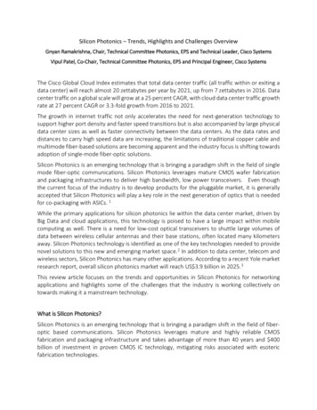
Silicon photonics technology allows formation of light guiding structures within an SOI siliconsubstrate and allows guiding, splitting, modulation and detection of light within a Silicon PhotonicsIC. Except for generation of light, Silicon Photonics can achieve all the remaining functions neededfor a transceiver for transmitting and receiving a digital signal to and from a single mode fiber opticcable.Silicon is a non-direct band gap material, and it is not possible to generate light efficiently in silicon.Hence, a Silicon Photonics IC is typically accompanied with a DC laser light source fabricated usingdirect band gap III-V materials. The laser source can be remote or can be integrated within theSilicon Photonics IC itself. 4 The photodiodes used for conversion of light into electrical signal (O-Econversion) are made using Ge, a material commonly available in the IC fabrication facilities. Themodulation of light (E-O conversion) is typically accomplished by a Mach Zehnder Interferometer(MZI) or with ring resonator design approaches. Fibers are attached to the Silicon Photonics IC tocarry light signals in and out of the waveguides of the Silicon Photonics IC using either surfacecoupling or edge coupling methods (Figure 1a).One of the key features of the Silicon Photonics is that various optical functional blocks such aswaveguides, modulators, mux/demux and detector are implemented using standard layout, DRC,LVS and simulation environment used for integrated circuit design/manufacturing (Figure 1b).Wafer level optical testing infrastructure is also developed by several IC fabrication housesallowing wafer level screening for yield management.Silicon Photonic ICTransceiver on a ChipCMOS/OSATMfg. InfrastructureFuture of OpticsCo-packaging with ASICsFigure 1: The promise of Silicon PhotonicsIn contrast to the traditional approach of using discrete optical elements with precisionplacements and costly alignments, Silicon Photonics enables wafer scale manufacturing of opticswith very high level of integration and scalability (Figure 1c). Silicon Photonics can be used in both1310nm (direct detect- within data centers) and 1550nm (coherent- between data centers andlong haul) wavelength categories and can support PAM4 and advanced coherent modulationschemes covering a wide spectrum of products.
Early products based on this technology relied on wire bonding to establish electrical connectionsbetween the electrical ICs (Driver, TIA, SERDES) and the Silicon Photonics IC. However, as the datarate and level of complexity have increased, more advanced packaging technologies such as 2.5Dintegration, TSVs, fanout technologies and 3D integration are being quicky adopted.Silicon Photonics based Pluggable Transceiver modulesThe industry adoption of Silicon Photonics based 100G modules has already started and isexpected to accelerate with 400G and beyond. Silicon photonics based direct detect as well ascoherent transceivers are being shipped by several vendors and roadmaps to develop SiliconPhotonics based higher speed and co packaged optics products have been shared by manycompanies. 5As the network connectivity speeds continue to increase to facilitate the enormous growth intraffic, the industry is witnessing a migration from 10G to 40G to 100G to 400G and beyond leadingto higher port density and faster speed transitions. This is accompanied by a higher level ofcomponent integration/packaging. The next generation form factors such as OSFP and QSFP-DDare targeted for 400G and 800G direct detect as well as 400G ZR coherent products. 6, 7 SiliconPhotonics based products are already being shipped or under development for CPAK, QSP28, OSFPQSFP-DD and QSFP800 form factors (Figure 2).22181411.612.49.54122189276929113016.2QSFP- DD400G/800G Modules100G Modules16OSFP5042CFP88335CFP4 QSFP28 uQSFP2921CFP2508675Line card faceplateCPAKCXP50CFP13.512.413.513.5Figure 2: Evolution of Pluggable ModulesData Center Evolution: From Pluggable to Co-Packaged OpticsASIC performance continues to follow the Moore’s law and doubles every two-three years. ASICcapacity is expected to increase from 12.6Tb to 25.2Tb to 51.4Tb and beyond, requiringcorresponding increase in the electrical signal speed of each I/O pin (input/output) and pin densityin the ASIC. With each new generation of ASIC, the challenge of moving the electrical signals acrossbecomes much greater as traditional metal wiring reaches its limits. To solve this challenge, theindustry is focusing on bring the optics closer and closer to the ASIC. Hence co-packaging of optics
and ASIC will become a necessity in the future to assure continued innovation in routing andswitching.OIF has already announced a project to address data rates around 224 Gbps 8 and it is widelybelieved that 102.4T switch ASIC will use 224 Gbps SerDes interface. According to a white paperby Rambus, integrating 800G optical engines in the same package as the switch ASIC will allow thesize, complexity, and power of the 112G SerDes to drop to extra short reach (XSR)requirements(Figure 3). Running at less than 1 picojoule per bit, XSR links reduce the I/O powerby more than 80% and the switch ASIC thermal design power (TDP) by more than 25% comparedto traditional short reach SerDes running at the same speed. 9Figure 3 : Co-packaging of 51.2 Tbps Switch ASICS- a conceptual drawing by RambusApplications of Silicon Photonics are not just limited to optical communication!!In addition to optical communication, Silicon Photonics has many applications in a wide range ofindustries that have the potential to revolutionize the world. These applications include opticalinterconnects and new architectures for high performance exascale super computers 10, lab on achip for biomedical testing and drug discovery 11, LIDARs for self driving cars 12, reconfigurableantennas for radars 13 as well as chip scale optical frequency combs for defense applications 14 toname a few. As the technology matures and eco system develops, Silicon Photonics is expected tofind many more applications. One of such notable application is development of Silicon Photonicsbased products for rapid testing and vaccine discovery for Covid-19 15.JEDEC Initiative to develop standards for Silicon Photonics reliabilityWhile high data rate pluggable modules and co-packaging are exciting developments that bringsa confluence of advances in semiconductor packaging such as 2,2.5D,3D heterogeneousintegration, optical alignments, thermal management and component and system level assemblyschemes and testing, in it lie many challenges as well. These challenges, viewed from a traditional
packaging framework, stem from selection of appropriate materials, integration schemes andarchitectures as well as to quantify and ensure testability and reliability. From the supply chainpoint of view, the eco system is very fragmented and developing quality and reliability standardsis a need of the hour to qualify and manage supply chain handoffs.By recognizing this need, JEDEC has recently formed Silicon Photonics Qualification and ReliabilityStandards Task Group (JC14) 16 with the goal of creating Silicon Photonics qualification andreliability standards (guidelines and methodology) within the JEDEC organization. The initial focusof this group is to develop requirements specific to Telecom Datacom. In the longer term, it plansto Include other industries using Silicon Photonics technology such as Automotive, Bio-medical,Sensing, Computing.ConclusionIn conclusion, the evolving Si-photonics technology offers a large opportunity to utilize innovationin electronic packaging technologies to meet the needs of the market currently driven by datacenters, telecom and many other upcoming verticals. This article looked into the trends inpluggable transceiver modules and upcoming trends in co-packaged optics.EPS Technical committee (TC) on Photonics aims to create a platform for conversation on this topicand would like to invite you to check for activities and updates on its webpagehttps://cmte.ieee.org/eps-pcsl/. The TC offers periodic webinars on related fields offered byleading industry experts and is a sponsor of the annual Reliability for Electronics and PhotonicPackaging symposium https://attend.ieee.org/repp/ .If you would like to contribute as a member into the committee, kindly contact the chair viaemail.For details on EPS – Photonics Technical committee, kindly send email tognyan.ramakrishna@ieee.orgSilicon Photonics: The future of High-Speed icon-photonics-the-future-of-high-speed-data/12 Siliconphotonics: the next onics-the-next-revolution/3 Siliconphotonics: datacom, yes, but not onlyhttp://www.yole.fr/Si Photonics Datacom Sensing.aspx4 IntelAdvances Progress in Integrated Photonics for Data C2020: The Future of Silicon Photonics and of-silicon-photonics-and-optics/6Verizon Media completes 400Gbit/s ZR trial with silicon photonics from Inphi
https://optics.org/news/11/9/397 Acaciasampling 400G pluggable optical transceiver modules including 400ZR, OpenZR andOpen ROADM MSAhttp://www.semiconductor-today.com/news items/2020/mar/acacia-100320.shtml8 OIFAnnounces 224 Gbps es-224-gbps-project-130500928.html9Data Center Evolution: From Pluggable To Co-Packaged Optics – White paper by from-pluggable-to-co-packaged-optics10 SiliconPhotonics for Extreme Scale ?tp &arnumber 863390311 On-chipwireless silicon photonics: from reconfigurable interconnects to lab-on-chip deviceshttps://www.nature.com/articles/lsa20175312 Anoverview of silicon photonics for t?SSO 113 Chip-basedphotonic radar for high-resolution 5.12802.pdf14 High-performancephotonics for defense takes a giant step forward, study -a-giant-step-forward-study-says15 ChasingCOVID-19 with 0/september/chasing covid19 with photonics/IEEE Photonics Standards Committee ds-Committee-June-18th-Meeting.pdf16
Silicon Photonics is an emerging technology that is bringing a paradigm shift in the field ofsingle mode fiber-optic communications. Silicon Photonics leverages mature CMOS wafer fabrication and packaging infrastructures to deliver high bandwidth, low power transceivers.