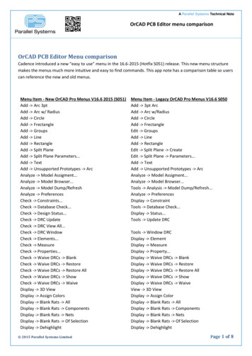
Transcription
OrCAD Flow TutorialProduct Version 16.2November 2008
1996–2008 Cadence Design Systems, Inc. All rights reserved.Portions Apache Software Foundation, Sun Microsystems, Free Software Foundation, Inc., Regents ofthe University of California, Massachusetts Institute of Technology, University of Florida. Used bypermission. Printed in the United States of America.Cadence Design Systems, Inc. (Cadence), 2655 Seely Ave., San Jose, CA 95134, USA.OrCAD Capture, OrCAD Capture CIS, PSpice, OrCAD Layout, and OrCAD PCB Editor contains technologylicensed from, and copyrighted by: Apache Software Foundation, 1901 Munsey Drive Forest Hill, MD 21050,USA 2000-2005, Apache Software Foundation. Sun Microsystems, 4150 Network Circle, Santa Clara,CA 95054 USA 1994-2007, Sun Microsystems, Inc. Free Software Foundation, 59 Temple Place, Suite330, Boston, MA 02111-1307 USA 1989, 1991, Free Software Foundation, Inc. Regents of the Universityof California, Sun Microsystems, Inc., Scriptics Corporation, 2001, Regents of the University of California.Daniel Stenberg, 1996 - 2006, Daniel Stenberg. UMFPACK 2005, Timothy A. Davis, University ofFlorida, (davis@cise.ulf.edu). Ken Martin, Will Schroeder, Bill Lorensen 1993-2002, Ken Martin, WillSchroeder, Bill Lorensen. Massachusetts Institute of Technology, 77 Massachusetts Avenue, Cambridge,Massachusetts, USA 2003, the Board of Trustees of Massachusetts Institute of Technology. All rightsreserved.Trademarks: Trademarks and service marks of Cadence Design Systems, Inc. contained in this documentare attributed to Cadence with the appropriate symbol. For queries regarding Cadence’s trademarks,contact the corporate legal department at the address shown above or call 800.862.4522.Open SystemC, Open SystemC Initiative, OSCI, SystemC, and SystemC Initiative are trademarks orregistered trademarks of Open SystemC Initiative, Inc. in the United States and other countries and areused with permission.All other trademarks are the property of their respective holders.Restricted Permission: This publication is protected by copyright law and international treaties andcontains trade secrets and proprietary information owned by Cadence. Unauthorized reproduction ordistribution of this publication, or any portion of it, may result in civil and criminal penalties. Except asspecified in this permission statement, this publication may not be copied, reproduced, modified, published,uploaded, posted, transmitted, or distributed in any way, without prior written permission from Cadence.Unless otherwise agreed to by Cadence in writing, this statement grants Cadence customers permission toprint one (1) hard copy of this publication subject to the following conditions:1. The publication may be used only in accordance with a written agreement between Cadence and itscustomer.2. The publication may not be modified in any way.3. Any authorized copy of the publication or portion thereof must include all original copyright,trademark, and other proprietary notices and this permission statement.4. The information contained in this document cannot be used in the development of like products orsoftware, whether for internal or external use, and shall not be used for the benefit of any other party,whether or not for consideration.Patents: The product, described in this document, are protected by U.S. Patents 5,481,695; 5,510,998;5,550,748; 5,590,049; 5,625,565; 5,715,408; 6,516,447; 6,594,799; 6,851,094; 7,017,137; 7,143,341;7,168,041.Disclaimer: Information in this publication is subject to change without notice and does not represent acommitment on the part of Cadence. Except as may be explicitly set forth in such agreement, Cadence doesnot make, and expressly disclaims, any representations or warranties as to the completeness, accuracy orusefulness of the information contained in this document. Cadence does not warrant that use of suchinformation will not infringe any third party rights, nor does Cadence assume any liability for damages orcosts of any kind that may result from use of such information.Restricted Rights: Use, duplication, or disclosure by the Government is subject to restrictions as set forthin FAR52.227-14 and DFAR252.227-7013 et seq. or its successor.
OrCAD Flow TutorialContents1Introduction to the tutorial. . . . . . . . . . . . . . . . . . . . . . . . . . . . . . . . . . . . . . . . . 7Objective of the tutorial . . . . . . . . . . . . . . . . . . . . . . . . . . . . . . . . . . . . . . . . . . . . . . . . . . . 7Audience . . . . . . . . . . . . . . . . . . . . . . . . . . . . . . . . . . . . . . . . . . . . . . . . . . . . . . . . . . . . 8Using the tutorial . . . . . . . . . . . . . . . . . . . . . . . . . . . . . . . . . . . . . . . . . . . . . . . . . . . . . . . . 8Installing design example . . . . . . . . . . . . . . . . . . . . . . . . . . . . . . . . . . . . . . . . . . . . . . . 8Terminology . . . . . . . . . . . . . . . . . . . . . . . . . . . . . . . . . . . . . . . . . . . . . . . . . . . . . . . . . 9What’s next . . . . . . . . . . . . . . . . . . . . . . . . . . . . . . . . . . . . . . . . . . . . . . . . . . . . . . . . . . . 10Recommended reading . . . . . . . . . . . . . . . . . . . . . . . . . . . . . . . . . . . . . . . . . . . . . . . . . . 102Creating a schematic design . . . . . . . . . . . . . . . . . . . . . . . . . . . . . . . . . . . . 11Objective . . . . . . . . . . . . . . . . . . . . . . . . . . . . . . . . . . . . . . . . . . . . . . . . . . . . . . . . . . . . .Design example . . . . . . . . . . . . . . . . . . . . . . . . . . . . . . . . . . . . . . . . . . . . . . . . . . . . . . . .Creating a design in Capture . . . . . . . . . . . . . . . . . . . . . . . . . . . . . . . . . . . . . . . . . . . . . .Guidelines . . . . . . . . . . . . . . . . . . . . . . . . . . . . . . . . . . . . . . . . . . . . . . . . . . . . . . . . .Creating a project . . . . . . . . . . . . . . . . . . . . . . . . . . . . . . . . . . . . . . . . . . . . . . . . . . . .Creating a flat design . . . . . . . . . . . . . . . . . . . . . . . . . . . . . . . . . . . . . . . . . . . . . . . . .Creating a hierarchical design . . . . . . . . . . . . . . . . . . . . . . . . . . . . . . . . . . . . . . . . . .Navigating through a hierarchical design . . . . . . . . . . . . . . . . . . . . . . . . . . . . . . . . . .Processing a design . . . . . . . . . . . . . . . . . . . . . . . . . . . . . . . . . . . . . . . . . . . . . . . . . . . .Adding part references . . . . . . . . . . . . . . . . . . . . . . . . . . . . . . . . . . . . . . . . . . . . . . . .Creating a cross reference report . . . . . . . . . . . . . . . . . . . . . . . . . . . . . . . . . . . . . . . .Generating a bill of materials . . . . . . . . . . . . . . . . . . . . . . . . . . . . . . . . . . . . . . . . . . .Getting your design ready for simulation . . . . . . . . . . . . . . . . . . . . . . . . . . . . . . . . . .Adding Layout-specific properties . . . . . . . . . . . . . . . . . . . . . . . . . . . . . . . . . . . . . . .Design rules check . . . . . . . . . . . . . . . . . . . . . . . . . . . . . . . . . . . . . . . . . . . . . . . . . . .Summary . . . . . . . . . . . . . . . . . . . . . . . . . . . . . . . . . . . . . . . . . . . . . . . . . . . . . . . . . . . . .What’s next . . . . . . . . . . . . . . . . . . . . . . . . . . . . . . . . . . . . . . . . . . . . . . . . . . . . . . . . . . .Recommended reading . . . . . . . . . . . . . . . . . . . . . . . . . . . . . . . . . . . . . . . . . . . . . . . . . .November 20083111212121316223737383942434547484949Product Version 16.2
OrCAD Flow Tutorial3Simulating a design. . . . . . . . . . . . . . . . . . . . . . . . . . . . . . . . . . . . . . . . . . . . . . . 51Objective . . . . . . . . . . . . . . . . . . . . . . . . . . . . . . . . . . . . . . . . . . . . . . . . . . . . . . . . . . . . .Simulation using PSpice . . . . . . . . . . . . . . . . . . . . . . . . . . . . . . . . . . . . . . . . . . . . . . . . .Files generated by PSpice . . . . . . . . . . . . . . . . . . . . . . . . . . . . . . . . . . . . . . . . . . . . .Analysis types . . . . . . . . . . . . . . . . . . . . . . . . . . . . . . . . . . . . . . . . . . . . . . . . . . . . . .Overview of the full adder design . . . . . . . . . . . . . . . . . . . . . . . . . . . . . . . . . . . . . . . .Simulating the full adder design . . . . . . . . . . . . . . . . . . . . . . . . . . . . . . . . . . . . . . . . . . . .Editing a simulation profile . . . . . . . . . . . . . . . . . . . . . . . . . . . . . . . . . . . . . . . . . . . . .Running PSpice . . . . . . . . . . . . . . . . . . . . . . . . . . . . . . . . . . . . . . . . . . . . . . . . . . . . .Viewing Output Waveforms . . . . . . . . . . . . . . . . . . . . . . . . . . . . . . . . . . . . . . . . . . . .Performing parametric analysis . . . . . . . . . . . . . . . . . . . . . . . . . . . . . . . . . . . . . . . . . . . .Adding a variable circuit parameter . . . . . . . . . . . . . . . . . . . . . . . . . . . . . . . . . . . . . .Adding a Plot Window Template marker . . . . . . . . . . . . . . . . . . . . . . . . . . . . . . . . . . .Setting up parametric analysis . . . . . . . . . . . . . . . . . . . . . . . . . . . . . . . . . . . . . . . . . .Running the simulation . . . . . . . . . . . . . . . . . . . . . . . . . . . . . . . . . . . . . . . . . . . . . . . .Exporting output waveforms . . . . . . . . . . . . . . . . . . . . . . . . . . . . . . . . . . . . . . . . . . . .Summary . . . . . . . . . . . . . . . . . . . . . . . . . . . . . . . . . . . . . . . . . . . . . . . . . . . . . . . . . . . . .What’s next . . . . . . . . . . . . . . . . . . . . . . . . . . . . . . . . . . . . . . . . . . . . . . . . . . . . . . . . . . .Recommended reading . . . . . . . . . . . . . . . . . . . . . . . . . . . . . . . . . . . . . . . . . . . . . . . . . .5252535458596060616869717173747575764Board design using OrCAD Layout . . . . . . . . . . . . . . . . . . . . . . . . . . . . . 77Overview . . . . . . . . . . . . . . . . . . . . . . . . . . . . . . . . . . . . . . . . . . . . . . . . . . . . . . . . . . . . .Objective . . . . . . . . . . . . . . . . . . . . . . . . . . . . . . . . . . . . . . . . . . . . . . . . . . . . . . . . . . . . .Preparations in Capture . . . . . . . . . . . . . . . . . . . . . . . . . . . . . . . . . . . . . . . . . . . . . . . . . .Running DRC . . . . . . . . . . . . . . . . . . . . . . . . . . . . . . . . . . . . . . . . . . . . . . . . . . . . . . .Creating Layout netlist . . . . . . . . . . . . . . . . . . . . . . . . . . . . . . . . . . . . . . . . . . . . . . . .Creating a board . . . . . . . . . . . . . . . . . . . . . . . . . . . . . . . . . . . . . . . . . . . . . . . . . . . . . . .Launch Layout . . . . . . . . . . . . . . . . . . . . . . . . . . . . . . . . . . . . . . . . . . . . . . . . . . . . . .Create the Layout board file . . . . . . . . . . . . . . . . . . . . . . . . . . . . . . . . . . . . . . . . . . . .Creating a board outline . . . . . . . . . . . . . . . . . . . . . . . . . . . . . . . . . . . . . . . . . . . . . . .Placing components . . . . . . . . . . . . . . . . . . . . . . . . . . . . . . . . . . . . . . . . . . . . . . . . . .Routing . . . . . . . . . . . . . . . . . . . . . . . . . . . . . . . . . . . . . . . . . . . . . . . . . . . . . . . . . . . . . .November 200847778797979808080868792Product Version 16.2
OrCAD Flow TutorialManual routing . . . . . . . . . . . . . . . . . . . . . . . . . . . . . . . . . . . . . . . . . . . . . . . . . . . . . . 92Autorouting using Layout . . . . . . . . . . . . . . . . . . . . . . . . . . . . . . . . . . . . . . . . . . . . . . 95Autorouting using SPECCTRA . . . . . . . . . . . . . . . . . . . . . . . . . . . . . . . . . . . . . . . . . . 95Post-processing . . . . . . . . . . . . . . . . . . . . . . . . . . . . . . . . . . . . . . . . . . . . . . . . . . . . . . . . 98Renaming components . . . . . . . . . . . . . . . . . . . . . . . . . . . . . . . . . . . . . . . . . . . . . . . 98Back annotation . . . . . . . . . . . . . . . . . . . . . . . . . . . . . . . . . . . . . . . . . . . . . . . . . . . . . 99Cross probing . . . . . . . . . . . . . . . . . . . . . . . . . . . . . . . . . . . . . . . . . . . . . . . . . . . . . . 100Generating output . . . . . . . . . . . . . . . . . . . . . . . . . . . . . . . . . . . . . . . . . . . . . . . . . . . . . 101Output files . . . . . . . . . . . . . . . . . . . . . . . . . . . . . . . . . . . . . . . . . . . . . . . . . . . . . . . . 102Reports . . . . . . . . . . . . . . . . . . . . . . . . . . . . . . . . . . . . . . . . . . . . . . . . . . . . . . . . . . . 103Summary . . . . . . . . . . . . . . . . . . . . . . . . . . . . . . . . . . . . . . . . . . . . . . . . . . . . . . . . . . . . 104What’s next . . . . . . . . . . . . . . . . . . . . . . . . . . . . . . . . . . . . . . . . . . . . . . . . . . . . . . . . . . 104Recommended reading . . . . . . . . . . . . . . . . . . . . . . . . . . . . . . . . . . . . . . . . . . . . . . . . . 1045Board design using OrCAD PCB Editor. . . . . . . . . . . . . . . . . . . . . . 105Overview . . . . . . . . . . . . . . . . . . . . . . . . . . . . . . . . . . . . . . . . . . . . . . . . . . . . . . . . . . . . 105Objective . . . . . . . . . . . . . . . . . . . . . . . . . . . . . . . . . . . . . . . . . . . . . . . . . . . . . . . . . . . . 106Preparations in Capture . . . . . . . . . . . . . . . . . . . . . . . . . . . . . . . . . . . . . . . . . . . . . . . . . 107Running DRC . . . . . . . . . . . . . . . . . . . . . . . . . . . . . . . . . . . . . . . . . . . . . . . . . . . . . . 107Creating PCB Editor netlist . . . . . . . . . . . . . . . . . . . . . . . . . . . . . . . . . . . . . . . . . . . . 107To know more about PCB Editor, see the PCB Editor tutorial. To open the tutorial, from theStart menu, choose Programs OrCAD 16.0 Tutorials PCB Editor Allegro PCBEditor Tutorial.Creating a board . . . . . . . . . . . . . . . . . . . . . . . . . . . . . . . . . . . . . . . . . 112Creating a board outline . . . . . . . . . . . . . . . . . . . . . . . . . . . . . . . . . . . . . . . . . . . . . . 112Adding mounting holes . . . . . . . . . . . . . . . . . . . . . . . . . . . . . . . . . . . . . . . . . . . . . . . 115Placing components . . . . . . . . . . . . . . . . . . . . . . . . . . . . . . . . . . . . . . . . . . . . . . . . . 118Routing . . . . . . . . . . . . . . . . . . . . . . . . . . . . . . . . . . . . . . . . . . . . . . . . . . . . . . . . . . . . . 121Manual routing . . . . . . . . . . . . . . . . . . . . . . . . . . . . . . . . . . . . . . . . . . . . . . . . . . . . . 122Autorouting using PCB Editor . . . . . . . . . . . . . . . . . . . . . . . . . . . . . . . . . . . . . . . . . . 126Autorouting using SPECCTRA for OrCAD . . . . . . . . . . . . . . . . . . . . . . . . . . . . . . . . 127Post-processing . . . . . . . . . . . . . . . . . . . . . . . . . . . . . . . . . . . . . . . . . . . . . . . . . . . . . . . 129Renaming components manually . . . . . . . . . . . . . . . . . . . . . . . . . . . . . . . . . . . . . . . 129Automatic Renaming of components . . . . . . . . . . . . . . . . . . . . . . . . . . . . . . . . . . . . 129Back annotation . . . . . . . . . . . . . . . . . . . . . . . . . . . . . . . . . . . . . . . . . . . . . . . . . . . . 132Cross probing and cross highlighting between PCB Editor and Capture . . . . . . . . . 136November 20085Product Version 16.2
OrCAD Flow TutorialGenerating output . . . . . . . . . . . . . . . . . . . . . . . . . . . . . . . . . . . . . . . . . . . . . . . . . . . . .Output files . . . . . . . . . . . . . . . . . . . . . . . . . . . . . . . . . . . . . . . . . . . . . . . . . . . . . . . .Reports . . . . . . . . . . . . . . . . . . . . . . . . . . . . . . . . . . . . . . . . . . . . . . . . . . . . . . . . . . .Summary . . . . . . . . . . . . . . . . . . . . . . . . . . . . . . . . . . . . . . . . . . . . . . . . . . . . . . . . . . . .What’s next . . . . . . . . . . . . . . . . . . . . . . . . . . . . . . . . . . . . . . . . . . . . . . . . . . . . . . . . . .Recommended reading . . . . . . . . . . . . . . . . . . . . . . . . . . . . . . . . . . . . . . . . . . . . . . . . .Glossary . . . . . . . . . . . . . . . . . . . . . . . . . . . . . . . . . . . . . . . . . . . . . . . . . . . . . . . . . .138139143143143144145Index. . . . . . . . . . . . . . . . . . . . . . . . . . . . . . . . . . . . . . . . . . . . . . . . . . . . . . . . . . . . . . . 149November 20086Product Version 16.2
Introduction to the tutorial1This chapter consists of the following sections: Objective of the tutorial Using the tutorial What’s next Recommended readingObjective of the tutorialTo enable users to evaluate the power of the OrCAD PCBtools used in the Windows-based PCB design process. Youcan use this tutorial to perform all the steps in the PCB designprocess. The tutorial focuses on the sequence of steps to beperformed in the PCB design cycle for an electronic design,starting with capturing the electronic circuit, simulating thedesign with PSpice, through the PCB layout stages, andfinishing with the processing of the manufacturing output andmaintaining the design through ECO cycles.Tasks covered in this tutorial may not cover all the features ofa tool. In this tutorial, the emphasis is on the steps that you willneed to perform in each OrCAD tool so that your design workssmoothly through the flow.OrCAD Flow Tutorial7
Chapter 1Introduction to the tutorialProduct Version 16.2The tutorial design example used in this tutorial works withinthe limits of the demo version of tools available in theOrCAD 16.2 CD.AudienceThis tutorial is useful for designers who want to use OrCADtools for the complete PCB design flow or for analogsimulation flow.You can also benefit from the tutorial if you are a first-time userof OrCAD Capture, PSpice, OrCAD Layout, OrCAD PCBEditor, or SPECCTRA for OrCAD.Using the tutorialTo run through the complete tutorial, you need the designexample and following tools: OrCAD Capture PSpice A/D OrCAD Layout or OrCAD PCB Editor SPECCTRA for OrCADAll these tools are available in the Unison Ultra suite exceptOrCAD PCB Editor, which is available in the OrCAD PCBDesigner suite .Note: This tutorial does not cover the tasks included inCapture CIS.Installing design exampleUnzip the flowtut.zip file provided with this tutorial.The design files are available at install dir /doc/flowtut/tutorial example.8OrCAD Flow Tutorial
Product Version 16.2Using the tutorialWhen you expand the design, the following directory structurewill be created.The partial directory contains files generated at the end ofChapter 2, “Creating a schematic design.” Use the files in thisdirectory only if you want to skip the design creation stepscovered in Chapter 2 and directly move on to Chapter 3 orChapter 4.The complete directory contains all the files generatedthrough all the chapters in this tutorial. You can use the files inthe complete directory to verify your results.TerminologyOrCAD Flow TutorialOrCAD CaptureOrCAD’s schematic designtoolCapture (initialCAPS)The terms OrCAD Captureand Capture have beenused interchangeably inthe tutorial.PSpiceOrCAD’s simulation tool,used for simulating bothAnalog and digital circuits.OrCAD LayoutOrCAD tool used for PCBrouting and floor-planningLayoutThe terms OrCAD Layoutand Layout have beenused interchangeably inthe tutorial.9
Chapter 1Introduction to the tutorialProduct Version 16.2OrCAD PCB EditorOrCAD tool used for PCBrouting and floor-planning.PCB EditorThe terms OrCAD PCBEditor and PCB Editorhave been usedinterchangeably in thetutorial.What’s nextIn the next chapter, Creating a schematic, you will useOrCAD Capture for creating a schematic design. You will learnto perform basic design tasks such as adding componentsfrom a library, adding wires, and getting your design ready forsimulation.Recommended readingFor more information about design suite configurationsprovided by OrCAD for affordable PCB design solutions, seethe OrCAD Unison Suites Flow Guide. For informationabout individual tools, see the respective User Guide.10OrCAD Flow Tutorial
Creating a schematic design2This chapter consists of the following sections: Objective Design example Creating a design in Capture Processing a design Summary What’s next Recommended readingObjectiveTo create a schematic design in OrCAD Capture. In thischapter, you will be introduced to basic design steps, such asplacing a part, connecting parts using wires, adding ports,generating parts, and so on.The steps for preparing your design for simulation usingPSpice and for taking your design for placement and routingto OrCAD Layout or OrCAD PCB Editor are also covered inthis chapter.OrCAD Flow Tutorial11
Chapter 2Creating a schematic designProduct Version 16.2Design exampleIn this chapter, you will create a full adder design in OrCADCapture. The full adder design covered in this tutorial is acomplex hierarchical design that has two hierarchical blocksreferring to the same half adder design.Duration:40 minutesCreating a design in CaptureGuidelinesWhen creating a new circuit design in OrCAD Capture, it isrecommended that you follow the guidelines listed below.121Avoid spaces in pathnames and filenames. This isnecessary to get your design into downstream products,such as SPECCTRA for OrCAD.2Avoid using special characters for naming nets, nodes,projects, or libraries. While naming nets, use of illegalcharacters listed below might cause the netlister to fail. ? (question mark) @ (at symbol) (telda) #(hash) & (ampersand) % (percent sign) “ (quotation marks) ! (exclamation mark) ( )(parenthesis) (smaller than)OrCAD Flow Tutorial
Product Version 16.2Creating a design in Capture (equal) (greater than) [ ](square parenthesis), * (asterisk)Creating a projectTo create a new project, we will use Capture's Project Wizard.The Project Wizard provides you with the framework forcreating any kind of project.1Launch Capture.2From the File menu, choose New Project.3In the New Project dialog box, specify the project name asFullAdd.4To specify the project type, select Analog or Mixed A/D.Note: An Analog or Mixed A/D project can easily besimulated using PSpice. It also ensures that your designflows smoothly into OrCAD Layout for your board design.5Specify the location where you want the project files to becreated and click OK.6In the Create PSpice Project dialog box, select theCreate a blank project option button.Note: When you create a blank project, the project canbe simulated in PSpice, but libraries are not configured bydefault. When you base your project on an existingproject, the new project has same configured libraries.7OrCAD Flow TutorialClick OK to create the FullAdd project with the abovespecifications.13
Chapter 2Creating a schematic designProduct Version 16.2TipIn case you already have a schematic design file(.dsn) that you want to simulate using PSpice, youneed to create an Analog or Mixed A/D project usingthe File New Project command and then addyour design to it.The FullAdd project is created. In the Project Managerwindow, a design file, fulladd.dsn, is created. Below thedesign file, a schematic folder with the name SCHEMATIC1 iscreated. This folder has a schematic page named PAGE1.Renaming the schematic folder and the schematic pageYou will now modify the design to change the name of both theschematic folder and the schematic page, to HALFADD.141In the Project Manager window, right-click onSCHEMATIC1.2From the pop-up menu, select Rename.3In the Rename Schematic dialog box, specify the nameas HALFADD.4Similarly, right-click on PAGE1 and from the pop-up menuselect Rename.5In the Rename Page dialog box, specify the page nameas HALFADD and click OK.OrCAD Flow Tutorial
Product Version 16.2Creating a design in CaptureAfter renaming of the schematic folder and the schematicpage, the directory structure in the Project Manager windowshould be to similar to the figure below.Using a design templateBefore you start with the design creation process in OrCADCapture, you can specify the default characteristics of yourproject using the design template. A design template can beused to specify default fonts, page size, title block, gridreferences and so on. To set up a design template in OrCADCapture, use the Design Template dialog box. To open the Design Template dialog box, from theOptions drop-down menu choose Design Template.To know more about setting up the design template, seeOrCAD Capture User’s Guide.OrCAD Flow Tutorial15
Chapter 2Creating a schematic designProduct Version 16.2Creating a flat designIn this section, we will create a simple flat half adder designwith X and Y as inputs and SUM and CARRY as outputs.Figure 2-1 Half adder designAdding partsTo add parts to your design:1From the Place menu in Capture, select Part.2In the Place Part dialog box, first select the library fromwhich the part is to be added and then instantiate the parton the schematic page.ImportantWhile working with the demo version of Capture, youwill add parts from EVAL.OLB. To add EVAL.OLB tothe project, select the Add Library button.16OrCAD Flow Tutorial
Product Version 16.2Creating a design in CaptureThe gates shown in Figure 2-1 on page 16 are availablein the 7400.OLB.TipUse the Part Search button in the Place Part dialogbox, to search the library to which the required partbelongs.To add 7400.OLB to the project, select the Add Librarybutton.3Browse to install dir /tools/capture/library/pspice/7400.olb.Select 7400.OLB and click Open.The 7400 library appears in the Libraries list box.4Browse to install dir /tools/capture/library/pspice/eval.olb.Select EVAL.OLB and click Open.OrCAD Flow Tutorial17
Chapter 2Creating a schematic designProduct Version 16.2The EVAL library appears in the Libraries list box.518From the Part List, select 7408 and click OK.OrCAD Flow Tutorial
Product Version 16.2OrCAD Flow TutorialCreating a design in Capture6Place three instances of the AND gate, 7408, on theschematic page as shown in the figure below.7Right-click and select End Mode.8Similarly, place an OR gate (7432) and two NOT gates(7404) as shown in the figure below.19
Chapter 2Creating a schematic designProduct Version 16.2Connecting partsAfter placing the required parts on the schematic page, youneed to connect the parts.1From the Place menu, choose Wire.The pointer changes to a crosshair.2Draw the wire from the output of the AND gate, U2A, tothe one of the inputs of the OR gate, U1B. To startdrawing the wire, click the connection point of the outputpin, pin3, on the AND gate.3Drag the cursor to input pin, pin4, of the OR gate (7432)and click on the pin to end the wire.Clicking on any valid connection point ends a wire.204Similarly, add wires to the design until all parts areconnected as shown in the figure below.5To stop wiring, right-click and select End Wire. Thepointer changes to the default arrow.OrCAD Flow Tutorial
Product Version 16.2Creating a design in CaptureAdding portsTo add input and output ports to the design, complete thefollowing sequence of steps:1From the Place menu in Capture, select HierarchicalPort.The Place Hierarchical Port dialog box appears.Note: Alternatively, you can select the Place port buttonfrom the Tool Palette.OrCAD Flow Tutorial2From the Libraries list box, select CAPSYM.3First add input ports. From the Symbols list, selectPORTRIGHT-R and click OK.4Place two instances of the port as shown in the figurebelow5Right-click and select End Mode.6To rename the ports to indicate input signals X and Y,double-click the port name.21
Chapter 2Creating a schematic design7Product Version 16.2In the Display Properties dialog box, change the value ofthe Name property to X and click OK.Note: You can also use the Property Editor to edit theproperty values of a component. To know the details, seeOrCAD Capture User’s Guide.8Similarly, change the name of the second port to Y.Note: You cannot use the Place Part dialog box for placingports, because ports in CAPSYM.OLB are onlysymbols and not parts. Only parts are listed in thePlace Part dialog box.9Add two output ports as shown in the figure below. To dothis, select PORTLEFT-L from the CAPSYM library.10 Rename the ports to SUM and CARRY, respectively.11 Save the design.The half adder design is ready. The next step is to create afull adder design that will use the half adder design.Creating a hierarchical designIn Capture, you can create hierarchical designs using one ofthe following methods: Bottom-up method Top-down methodAnother method of creating a hierarchical design is to createparts or symbols for the designs at the lowest level, and savethe symbols in a user-defined library. You can later add theuser-defined library in your projects and use these symbols inthe schematic. For example, you can create a part for the halfadder design and then instead of hierarchical blocks, use thispart in the schematic. To know more about this approach, seeGenerating parts for a schematic.In this section, we will create the full adder hierarchical design.The half adder design created in the Creating a flat designsection will be used as the lowest level design.22OrCAD Flow Tutorial
Product Version 16.2Creating a design in CaptureBottom-up methodWhen you create a hierarchical design using the bottom-upmethodology, you need to follow these steps. Create the lowest-level design. Create higher-level designs that instantiate thelower-level designs in the form of hierarchical blocks.In this section, we will create a full adder design usingbottom-up methodology. The steps involved are:1Creating a project in Capture. To view the steps, seeCreating a project on page 13.2Creating the lowest-level design. In the full adder designexample, the lowest-level design is the half adder design.To go through the steps for creating the half adder
of OrCAD Capture, PSpice, OrCAD Layout, OrCAD PCB Editor, or SPECCTRA for OrCAD. Using the tutorial To run through the complete tutorial, you need the design example and following tools: OrCAD Capture PSpice A/D OrCAD Layout or OrCAD PCB Editor SPECCTRA for OrCAD All these tools are available in the Unison Ultra suite except OrCAD PCB Editor .