Transcription
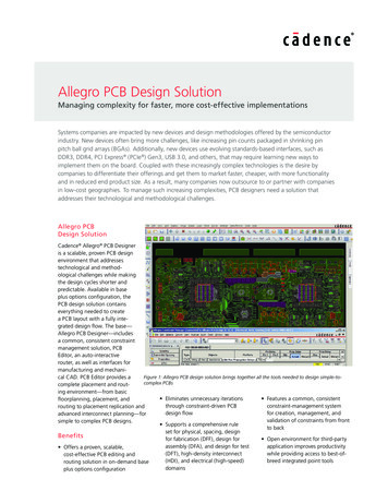
OrCAD PCB DesignerReal-Time PCB Design, High Speed Signal Routing, DesignTrue DFM, Interactive 3DThe OrCAD PCB design solution provides everything you needto take your PCB designs from concept to production. Trulyscalable and production proven in every market segment fromsmart-home controllers through industrial robotics to automotiveand spacecraft, the OrCAD PCB Designer Standard and OrCADPCB Designer Professional products help you stay competitive intoday’s electronics market. The OrCAD PCB design solution helpsyou manage the challenges in real-time of shorter design cycles,high speed signal routing, DesignTrue DFM, emerging Rigid-Flexsubstrates, and a faster time to market to achieve your designgoalsOverviewOrCAD PCB Designer Standard and OrCAD PCB DesignerProfessional, provide a tiered, scalable PCB design solutionthat delivers advanced capabilities and highly integrated flows.Whether your designs are simple or more sophisticated withhigher densities, complex rules, mixed-signal circuits, and/orstandards-based interfaces, the OrCAD PCB design solution haseverything you need to increase your team’s productivity andefficiency while reducing your overall costs and time to market.The OrCAD PCB design solution can not only be tailored toaddress your specific design needs but also your budget requirements; maximizing your investment with a low cost of entryand ownership. The powerful, tightly integrated PCB designtechnologies include schematic capture, librarian tools, PCBediting/routing, single, consistent front-to-back ConstraintManager environment, signal integrity exploration, autorouting(Professional), High-speed and Backdrilling rules (Professional),Rigid-Flex circuit support, and optional mixed-signal circuitsimulation. Easy-to-use and intuitive, they offer exceptional valueand future-proof scalability to the Cadence Allegro series ofPCB design products.Highlights Proven, scalable, easy-to-use PCB editing androuting solution that grows as design challengesand requirements evolve TÜV SÜD “Fit for Purpose – TCL1” certified tomeet ISO26262 automotive functional safetyrequirements Shorten time to identify and fix high speed signalsin real-time using visual feedback for Real-timeImpedance, Real-time Coupling and Real-time Route Save significant time using Backdrilling rules and realtime checks for clearances with backdrill markedvias and pins OrCAD PCB Designer Professional is now HighSpeed Aware leveraging Dynamic Diff Pair Phasecontrol, Pin Delay Property, Z-Axis Delay, Nested NetGroups, etc Constraint Manager provides real-time validationand status of physical/spacing, same net, region,differential pair, and length rules to help ensurefirst-time success Automatic and interactive etch editing deliversintelligent automation to maintain user controlwhile maximizing productivity Dynamic real-time copper pour plowing and healingto eliminate error-prone manual voiding and rework Rigid-Flex design support with cross-section stackupby zone, Flex bend editor, ARC route editing, andRigid-Flex-specific DRCs Support for IPC-2581, STEP, and IDX brings a levelof intelligence and integration that streamlinesmanufacturing and MCAD-ECAD flows
OrCAD PCB DesignerAutomotive TCL1 Certified for ISO 26262The industry’s first PCB design and verification flow to achieve “Fit for Purpose - Tool Confidence Level 1 (TCL1)” certification enablesyou to meet stringent ISO 26262 automotive safety requirements. The flow includes everything from design authoring to simulationto physical realization and verification using the PSpice , Allegro, and OrCAD product suites. The high-performance design entry,simulation, and layout editing tools provide an integrated environment for design engineers to validate the safety specificationsagainst individual circuit specifications for design confidence. For information on the safety manuals, Tool Confidence Analysis (TCA)documents, and compliance reports from TÜV SÜD, download the Functional Safety Documentation Kits through Cadence OnlineSupport.Powerful FloorplanningAt the heart of the OrCAD PCB design solution is OrCAD PCB Editor, an easy-to-use, interactive place-and-route environmentfor creating and editing simple to complex PCBs. The extensive feature set addresses a wide range of today’s modern design andmanufacturability challenges. This powerful and flexible set of features includes automatic, schematic-driven floorplanning and interactive placement, intelligent interactive routing, dynamic shapes, placement replication, simple and advanced rules (including differential pairs, length, region, layer, etc.), STEP model support and 3D viewing, and MCAD-ECAD (interfaces for manufacturing andmechanical CAD).STEP models provide a realistic three dimensionalrepresentation of your designFloorplanning and placementAutomatic, schematic-driven floorplanning and interactive-placement capabilities are designed to accelerate parts placement.Components or subcircuits are assigned to specific “rooms” during design entry to facilitate automatic floorplanning. In interactiveplacement, components can be filtered and selected in a wide variety of ways to streamline the placement process: by reference designator, device package and footprint style, associated net name, part number, or the schematic sheet/page number.Interactive etch editingInteractive routing capabilities deliver controlled automation while maximizing routing productivity. Real-time, shape-based, andany-angle push and shove routing methods address a wide array of routing challenges. The routing engine optimizes traces by eitherpushing obstacles or following contours while dynamically jumping over obstacles such as vias or component pins. Routing modesinclude “shove-preferred,” “hug-preferred,” or “hug-only.” The shove-preferred mode constructs the optimum trace path whiledynamically pushing obstacles or automatically “jumping” over obstacles such as pins or vias. The hug-preferred mode is the perfectsolution when a databus must be constructed. In this mode, the trace contour follows other traces as a priority and only pushes asideor jumps over obstacles when there is no other option.Backdrilling in PCB Designer ProfessionalUsers can now specify which vias on critical high-speed signals should be back drilled to avoid reflections. An output report—BackdrillNC and Legend Files from Bottom, Top, or Any Layer if backdrilling the inner core(s) of the PCB—allows users to send backdrillinginstructions to their PCB manufacturers2
OrCAD PCB DesignerDynamic copper shapesDynamic copper shape technology offers real-time copper pour plowing and healing functionality. Shape parameters can be applied atthree different levels: global, shape instance, and object-level hierarchies. Traces, vias, and components added to a dynamic shape willautomatically plow and void through the shape. When items are removed, the shape automatically fills back in. Dynamic shapes do notrequire batch autovoiding or other post-processing steps after edits are made.Placement replication and reuseIntelligent placement replication technology enables you to automatically place and route replicated circuits using a seed circuit that isapplied to other circuit instances within the design. Changes made to the seed circuit are automatically propagated to the duplicatedcircuits. Circuit templates with “known-good” placement and routing can be reused in other designs with similar circuits.Constraint ManagerDesign rules and electrical and physical constraints are more critical to your projects’ success than ever before. Dealing with all thecomplexities of the rules and constraints of a modern design requires a powerful constraint management system capable of coveringall the aspects of creation, management, and validation. The OrCAD PCB constraint management system displays physical/spacing,samenet, region, and differential pair and length rules along with their status (based on the current state of the design) in real timeand is available at all stages of the layout process. Each worksheet provides a spreadsheet interface that enables you to easily define,manage, and validate the different rules in a hierarchical fashion.The constraint management system is completely integrated within the OrCAD PCB design solution, and constraints can be validatedin real time as the design process proceeds. The result of the validation process is a graphical representation of whether constraintspass (highlighted in green) or fail (highlighted in red). This approach allows you to immediately see the progress of the design in thespreadsheets, as well as the impact of any design changes.High Speed Constraints-Driven Autorouting in PCB Designer ProfessionalIncreasing use of standards-based advanced interfaces such as DDR3, DDR4, PCIe, USB 3.0 are bringing a set of constraints that mustbe adhered to while implementing a PCB. The OrCAD PCB Designer Professional now makes adhering to high speed constraints onadvanced interfaces quick and easy. High-speed routing constraints and algorithms handle differential pairs, pin delay, nested netgroups, Z-axis delay requirements demanded by today’s high-speed circuits. The autorouting algorithms intelligently handle routingaround or through vias, and automatically conform to defined length criteria. Separate design rules may be applied to different regionsof the design; for example, you can specify tight clearance rules in the connector area of a design and less stringent rules elsewhere.Real Time PCB Design will shorten time to identity and fix High Speed signals in Real-time with visual feedback using Real-TimeImpedance, Real-Time Coupling and Real-Time Route. This is an innovative and unique environment that allows users to graphicallysee real time delay and phase information directly on the routing canvas. Traditionally, evaluating current status of length of a routedinterface required numerous trips to Constraint Manager and/or use of the Show Element command. Using an embedded route engineto evaluate complex timing constraints and interdependencies amongst signals shows current status of a set of routed signals—a DDRxbyte lane or a complete DDRx interface— via custom trace/connect line coloring; stipple patterns and customized data tip informationto define the delay problem in the simplest terms possible. This functionality is now available in the OrCAD PCB Designer Professional.STEP models provide a realistic three dimensionalrepresentation of your designReal-Time CouplingReal time RouteDesigning Rigid-FlexRigid-Flex substrates are becoming common in IoT, wearables, and mobile smart devices as well as inmedical devices and even automotive. In the OrCAD PCB Layout editors, a designer can define multiplesubstrate material cross-sections as well as area- dependent rules to meet Rigid-Flex design and3
OrCAD PCB Designermanufacturing guidelines. New Flex focus arc routing and Flex bend editor provide the designer with the necessary tools to managethe complex Rigid-Flex or pure Flex designs.3D Display and VisualizationThe OrCAD 3D viewer environment gives you the ability to see a realistic, three-dimensional representation of your design. Theenvironment supports several filtering options, camera views, graphic display options such as solid, transparency and wireframe, andcontrols for panning, zooming, and spinning the display. 3D viewing also supports the display of complex via structures or isolatedsections of the board for viewing more details. With support for the STEP format and models, the OrCAD PCB design solutionsupports the import of model-accurate component and mechanical elements, such as an enclosure, to view in the context of your PCBproject. This allows you to perform visual clearance checks to detect clashes early on and ensure you will have proper fit when youmove to manufacture.PCB ManufacturingThe OrCAD PCB design solution supports a full suite of phototooling and bare-board fabrication, and test outputs can be generatedincluding Gerber 274x, NC drill, and bare-board test in a variety of formats. The OrCAD PCB design solution also supports the industryinitiative toward Gerber-less manufacturing through the export (and import) of design data in the IPC-2581 format. The IPC-2581 datais passed in a single file that creates accurate and reliable manufacturing data for high-quality manufacturing. You have a choice toexport a subset of the design data for protecting design IP.Design Solutions and FlowsTopology exploration with signal integrity analysisIncluded with the OrCAD PCB Designer is the Allegro Sigrity SI SigXplorer, which provides a graphical view of I/O buffers, transmissionlines, and vias such that complex topologies can be modified in a what-if fashion without having to change the actual design.SigXplorer also allows engineers to sweep various parameters within the topology to identify a topology solution space. With theOrCAD PCB Designer Professional product, routed or unrouted topologies can be extracted directly from the PCB design database,enabling you to simulate critical nets to validate that the layout work matches the pre-route requirements. Topology extraction canbe performed at three key stages for signal-quality prediction and analysis: during part placement (pre-route), after routing criticalnets, and after final routing of the design. Topologies are extracted back into the SigXplorer canvas that was used to analyze the netduring pre-route, and the routed signal’s analysis is compared to the expected results. The extraction includes a detailed electricalrepresentation of how the net was physically implemented, including models for trace cross-sectional characteristics, routing layers, viamodels, and trace lengths. If the results do not match, the routed board can be modified and the net re-analyzed.MCAD-ECAD collaborationThe proven and industry-adopted IDX-based ECAD-MCAD collaboration in the OrCAD PCB design solution allows you to intelligently4
OrCAD PCB Designerand interactively synchronize on incremental changes between the electrical and mechanical design environments.Unlike interim file formats such as IDF and DXF, IDX formats give you the ability to preview and analyze changes graphically beforeaccepting or rejecting the data. Additionally, designers in both environments can choose to accept or reject the proposed changes onan object-by-object basis as well as offer counter- proposal changes. This level of interaction provides a degree of control and collaboration that was previously not possible and helps ensure the two environments remain in sync. It also helps to avoid any miscommunication that can result in rework and significantly improves the chances of first-time success.Automatic routingOrCAD PCB Designer Professional is tightly integrated with Cadence SPECCTRA for OrCAD, the market-leading PCB solution forautomatic and auto-interactive interconnect routing. Designed to handle routing challenges from contemporary designs to highdensity multilayer PCBs requiring complex design rules, SPECCTRA for OrCAD uses powerful shape-based algorithms to make themost efficient use of the routing area.The results are increased completion rates, higher productivity, and shorter design cycle times.Future-Proof ScalabilityUnlike other PCB design solutions, the OrCAD PCB design solution has the ability to grow with your evolving technology challengesand as your place and route needs change. Based on Allegro PCB design technology, the OrCAD PCB design solution provides thesecurity of scalability to meet those challenges easily. Features and technologies are shared across the OrCAD and Allegro productlines, allowing products to be easily upgraded and expanded without the need to translate databases or libraries, learn new applications, or change use models.For the latest product or release information, visit us atwww.orcad.com or contact your local Cadence Channel Partner.Sales, Technical Support, and TrainingThe OrCAD product line is owned by Cadence Design Systems, Inc., and is supported by a worldwide network of Cadence ChannelPartners (VARs). For sales, technical support, or training, contact your local channel partner. For a complete list of authorized channelpartners, visit www.orcad.com/CCP-Listing.www.orcad.com 2018 Cadence Design Systems, Inc. All rights reserved worldwide. Cadence, the Cadence logo, Allegro, SPECCTRA, and OrCAD are registered trademarks and the OrCAD logo is a trademark of CadenceDesign Systems, Inc. in the United States and other countries. All other trademarks are the property of their respective owners.
OrCAD PCB Designer Standard and OrCAD PCB Designer Professional, provide a tiered, scalable PCB design solution Whether your designs are simple or more sophisticated with higher densities, complex rules, mixed-signal circuits, and/or standards-based interfaces, the OrCAD PCB design solution has everything you need to increase your team's .