Transcription
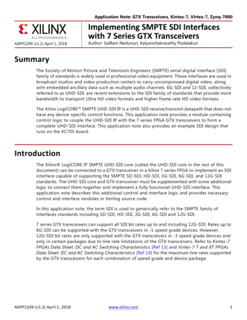
Application Note: GTX Transceivers, Kintex-7, Virtex-7, Zynq-7000XAPP1249 (v1.2) April 1, 2018Implementing SMPTE SDI Interfaceswith 7 Series GTX TransceiversAuthor: SaiRam Nedunuri, Kalyanchakravathy PodalakuriSummaryThe Society of Motion Picture and Television Engineers (SMPTE) serial digital interface (SDI)family of standards is widely used in professional video equipment. These interfaces are used inbroadcast studios and video production centers to carry uncompressed digital video, alongwith embedded ancillary data such as multiple audio channels. 6G-SDI and 12-SDI, collectivelyreferred to as UHD-SDI, are recent extensions to the SDI family of standards that provide morebandwidth to transport Ultra HD video formats and higher frame rate HD video formats.The Xilinx LogiCORE SMPTE UHD-SDI IP is a UHD-SDI receive/transmit datapath that does nothave any device-specific control functions. This application note provides a module containingcontrol logic to couple the UHD-SDI IP with the 7 series FPGA GTX transceivers to form acomplete UHD-SDI interface. This application note also provides an example SDI design thatruns on the KC705 board.IntroductionThe Xilinx LogiCORE IP SMPTE UHD-SDI core (called the UHD-SDI core in the rest of thisdocument) can be connected to a GTX transceiver in a Xilinx 7 series FPGA to implement an SDIinterface capable of supporting the SMPTE SD-SDI, HD-SDI, 3G-SDI, 6G-SDI, and 12G-SDIstandards. The UHD-SDI core and GTX transceiver must be supplemented with some additionallogic to connect them together and implement a fully functional UHD-SDI interface. Thisapplication note describes this additional control and interface logic and provides necessarycontrol and interface modules in Verilog source code.In this application note, the term SDI is used to generically refer to the SMPTE family ofinterfaces standards including SD-SDI, HD-SDI, 3G-SDI, 6G-SDI and 12G-SDI.7 series GTX transceivers can support all SDI bit rates up to and including 12G-SDI. Rates up to6G-SDI can be supported with the GTX transceivers in -1 speed grade devices. However,12G-SDI bit rates are only supported with the GTX transceivers in -3 speed grade devices andonly in certain packages due to line rate limitations of the GTX transceivers. Refer to Kintex-7FPGAs Data Sheet: DC and AC Switching Characteristics [Ref 13] and Virtex-7 T and XT FPGAsData Sheet: DC and AC Switching Characteristics [Ref 14] for the maximum line rates supportedby the GTX transceivers for each combination of speed grade and device package.XAPP1249 (v1.2) April 1, 2018www.xilinx.com1
IntroductionThe primary functions of the device-specific SDI control logic provided with this applicationnote are: Reset logic for the GTX transceiver Dynamic switching of the GTX RX and TX serial clock dividers to support the five SDIstandards Dynamic RX and TX reference clock switching to support two different bit rates in each ofthe HD-SDI, 3G-SDI, 6G-SDI, and 12G-SDI standards 1.485 Gb/s and 1.485/1.001 Gb/s in HD-DI mode 2.97 Gb/s and 2.97/1.001 Gb/s in 3G-SDI mode 5.94 Gb/s and 5.94/1.001 Gb/s in 6G-SDI mode 11.88 Gb/s and 11.88/1.001 Gb/s in 12G-SDI modeDynamic switching of the GTX RXDATA and TXDATA port widths 20-bit RXDATA and TXDATA ports for SD-SDI, HD-SDI, and 3G-SDI modes 40-bit RXDATA and TXDATA ports for 6G-SDI and 12G-SDI modes Data recovery unit for recovering data in SD-SDI mode RX bit rate detection to determine if the RX is receiving integer frame-rate signals (linerates such as 1.485 Gb/s and 2.97 Gb/s) or fractional frame-rate signals (line rates such as1.485/1.001 Gb/s and 2.97/1.001 Gbs)Also supplied with this application note is a wrapper file that contains a GTX transceiverinstance, an instance of the control module, and an instance of the SMPTE UHD-SDI core withthe necessary connections between them. This file simplifies the process of creating an SDIinterface.This application note includes an example SDI design using the UHD-SDI core. This exampledesign runs on the KC705 evaluation board. A Fidus 12G-SDI FPGA mezzanine card (FMC) is alsorequired to provide the UHD-SDI physical interfaces.In this document, the following terms are used. The UHD-SDI core refers to the SMPTE UHD-SDIcore that is available in the Vivado tool IP catalog starting with 2015.1 release. The controlmodule is a module that implements the various device-specific functions when using the GTXto implement an UHD-SDI interface using the UHD-SDI core. The control module is supplied onsource code form with this application note. The GTX wrapper is a wrapper file for a single GTXtransceiver generated by the 7 Series FPGAs Transceivers Wizard that is available in the IPcatalog. The GTX common wrapper is a wrapper file containing the QPLL for the GTX Quad alsogenerated by the 7 Series FPGAs Transceivers Wizard when the GTX wrapper is generated. TheSDI wrapper is a wrapper module that instances and interconnects the SMPTE UHD-SDI core,the GTX wrapper, and the control module. The SDI wrapper is supplied in source code form withthis application note. The GTX common wrapper is not included in the SDI wrapper and must beinstantiated separately in the application. Figure 1 is a simplified block diagram of how thevarious pieces fit together to form an UHD-SDI interface.XAPP1249 (v1.2) April 1, 2018www.xilinx.com2
FeaturesX-Ref Target - Figure 1Optional AudioEmbedder210 16TX ClockTX VideoTX ST352 PIDTX SDI Mode10 1632 83Kintex-7 FPGA10 16SDI WrapperSMPTEUHD-SDICoretxusrclk40RX Videotxusrclk2Cable DriverSDI OutResets & ControlCable EqualizerStatusRX StatusRX ST352 PIDBUFGtxoutclktxdataTX ControlRX SDI ModeGTX Wrapper40332 810 16EQrxdataControlModulerxusrclkrxusrclk2SDI InBUFGrxoutclkCPLL refclksRX ClockGTX CommonWrapper148.5 MHz148.5/1.001 MHzReference Clock SourceFigure 1:Block Diagram of a Complete UHD-SDI RX/TX InterfaceFeaturesThe LogiCORE IP SMPTE UHD-SDI Product Guide [Ref 16] lists all the features of the UHD-SDIcore and SMPTE standards supported by the core. Please refer to that document for moreinformation. That document also has timing diagrams showing the input and output timing ofthe core in the various SDI modes.This document uses the term elementary data streams to refer to an SDI data stream that is notmultiplexed. For example, an HD-SDI signal consists of two elementary data streams, usuallyreferred to as the Y and C data streams, that are multiplexed together onto the virtual 10-bitHD-SDI interface. Likewise, a 3G-SDI level A signal also consists of two elementary data streams,called data stream 1 and data stream 2, that are multiplexed together onto the 10-bit virtual3G-SDI interface. A 3G-SDI level B signal, however, consists of four elementary data streams, aY and a C data stream for each of the HD-SDI signals that are aggregated together onto the3G-SDI level B interface. These four elementary streams get interleaved in a 4-way multiplexonto the 10-bit virtual 3G-SDI interface. With the introduction of 6G-SDI and 12G-SDI, up to 16elementary data streams may be interleaved onto a single SDI interface. These data streams arecalled ds1 through ds16 in this document and in the port names of the UHD-SDI core and theUHD-SDI wrapper.XAPP1249 (v1.2) April 1, 2018www.xilinx.com3
Using 7 Series GTX Transceivers for SDI InterfacesThe UHD-SDI core TX only accepts and the RX only outputs elementary, non-multiplexed, datastreams on its data stream inputs and outputs. The multiplexing and de-multiplexing of datastreams occurs internally to the UHD-SDI core and is not something that must be dealt withoutside of the core. SD-SDI is an exception to this. The ST 259 SD-SDI standard defines a singledata stream that carries both the Y and C components. This is considered to be an elementarydata stream by the UHD-SDI core because multiple EAVs and SAVs are not interleaved.The UHD-SDI core does not do any mapping between native video formats and elementary datastreams. The user application must do any necessary mapping of video to elementary datastreams prior to providing those streams to the UHD-SDI transmitter and must reconstruct thevideo image from the elementary streams output by the UHD-SDI receiver. For all video formatson SD-SDI and single-link HD-SDI and for 1080p 50, 59.94, and 60Hz 4:2:2 YCbCr 10-bit videoon 3G-SDI level A, no mapping is necessary because there is a one-to-one correspondencebetween the data streams of these formats and the elementary data streams into and out of theUHD-SDI core. This is also true for 3G-SDI level B-DS, the dual stream mode where two HD-SDIvideo formats are aggregated onto a single 3G-SDI interface. For dual-link HD-SDI, 3G-SDI levelB-DL, multi-link 3G-SDI, 6G-SDI, and 12G-SDI, mapping of the video formats to and fromelementary data streams is required and is not done in the UHD-SDI core.For 6G-SDI, the UHD-SDI core supports up to 8 elementary data streams. For 12G-SDI, theUHD-SDI core supports up to 16 elementary data streams. In the SMPTE 6G-SDI and 12G-SDImapping documents, the term "data streams" refers to both multiplexed and non-multiplexed(elementary) data streams and care must be used when interpreting these documents todetermine how many elementary data streams are used by each mapping method. Dependingon the data format being transported, either four or eight elementary data streams areinterleaved together on a 6G-SDI interface and either eight or sixteen elementary data streamsare interleaved together on a 12G-SDI interface. The 16-way interleave only occurs in dual link12G-SDI. The UHD-SDI TX must be told how many streams are active on its input using the portcalled tx mux pattern. The UHD-SDI RX automatically determines how many elementary datastreams are present in the incoming SDI signal, demultiplexes the data stream appropriately,and indicates on the rx active streams port how many elementary data streams are present inthe incoming signal.Using 7 Series GTX Transceivers for SDI InterfacesThis section describes the details of implementation UHD-SDI interfaces using GTX transceiversin Xilinx 7 series FPGA devices (Kintex -7, Virtex -7, and Zynq -7000).The information in this section is intended to supplement, not replace, the information in7 Series GTX/GTH Transceivers User Guide [Ref 15]. This information highlights features of theGTX transceivers that are of particular importance for UHD-SDI applications.There are several clocks required in applications using GTX transceivers. The SDI protocol doesnot allow for clock correction by adding and removing extra data in the data stream. Therefore,careful attention is required regarding how these clocks are generated and used in theapplication. GTX transceivers require reference clocks to operate. The reference clocks are usedby phase-locked loops (PLLs) in the GTX transceiver Quad to generate serial clocks for theXAPP1249 (v1.2) April 1, 2018www.xilinx.com4
Using 7 Series GTX Transceivers for SDI Interfacesreceiver and transmitter sections of each transceiver. As described in more detail in the GTXTransceiver Reference Clocks section, the serial bit rate of the GTX transmitter is an integermultiple of the reference clock frequency it is using. Furthermore, the data rate of the videoprovided to the input of the UHD-SDI transmitter datapath must also exactly match (or be aspecific multiple of) the frequency of the reference clock used by the GTX transmitter.Consequently, a UHD-SDI application must generate the transmitter reference clock so that it isfrequency-locked exactly with the data rate of the video stream being transmitted.The GTX transmitter outputs a clock on its txoutclk port at a frequency that is exactly equal tothe word rate of the data that must enter the txdata port of the GTX transmitter. The txoutclk isgenerated in the GTX transmitter by dividing the serial clock from the PLL down to the wordrate. In most applications, the txoutclk from the GTX transmitter is buffered by a global (BUFG)clock buffer and then used to clock the UHD-SDI transmitter datapath and the txusrclk andtxusrclk2 clock inputs of the GTX transmitter. It is possible to use a clock other than one deriveddirectly from txoutclk as the clock source for the UHD-SDI transmitter datapath and the txusrclkand txusrclk2 ports of the GTX transmitter. A shallow TX buffer in the GTX transmitter does allowfor phase differences between the data entering the txdata port and the internal clock of theGTX transmitter. However, any frequency difference between the incoming data and the internalclock frequency of the GTX transmitter (as represented by txoutclk) quickly causes the TX bufferto underflow or overflow, resulting in errors in the serial bitstream generated by the GTXtransmitter. Consequently, the data rate of the data stream entering the txdata port of the GTXtransmitter (as represented by the frequency of the txusrclk and txusrclk2 clocks) and theinternal data rate of the GTX transmitter (as set by the transmitter reference clock andrepresented by the frequency of txoutclk) must match exactly.The GTX receiver reference clock, however, does not need an exact relationship with the linerate of the incoming SDI signal. This is because the clock and data recovery (CDR) unit in theGTX receiver can receive lines rates that are up to 1250 ppm away from the nominal bit rate asset by the reference clock frequency in all modes except 12G-SDI. In 12G-SDI mode, the linerate of the 12G-SDI signal must be within 200 ppm of the nominal line rate as set by thereference clock frequency. This allows the receiver reference clock to be generated by a localoscillator that has no exact frequency relationship to the incoming SDI signal. The GTX receivergenerates a recovered clock that is frequency-locked to the incoming SDI bit rate. This clock isoutput on the rxoutclk port of the GTX transceiver. As is described in more detail later in thisapplication note, rxoutclk is a true recovered clock when receiving any SDI signal exceptSD-SDI. Typically, rxoutclk is buffered by a global clock buffer and then applied to the rxusrclkand rxusrclk2 ports of the GTX receiver and used as the clock for the UHD-SDI receiverdatapath.One additional clock is required for SDI applications. This is a free-running, fixed-frequencyclock that is used as the clock for the dynamic reconfiguration port (DRP) of the GTXtransceiver. This same clock is also usually supplied to the control module in the SDI wrapperwhere it is used for timing purposes. Xilinx recommends that the frequency of this clock be atleast 10 MHz. The maximum frequency of this clock is limited by the maximum allowed DRPclock frequency of the GTX transceiver, which is speed grade dependent. The frequency of thisclock does not require any specific relationship relative to other clocks or data rates of the SDIapplication. This clock must not change frequencies when the SDI mode changes. It mustremain running at the same nominal frequency at all times. It also must never stop while the SDIapplication is active. This clock can be used for all SDI interfaces in the device.XAPP1249 (v1.2) April 1, 2018www.xilinx.com5
Using 7 Series GTX Transceivers for SDI InterfacesThe frequency of the rxoutclk and txoutclk depend on the SDI mode and the width of the GTXtransceiver's rxdata and txdata ports. This relationship is fixed by the architecture of the GTXtransceiver. The RX and the TX both use clock enables to throttle the data stream transfer datarate because, in some cases, the data rate on the data streams is less than the frequency of theclock. Table 1 shows the relationships between SDI mode, number of active data streams,rxdata/txdata port widths, rxoutclk/txoutclk frequencies, and clock enable cadences. The clockenable cadences are given in number of clocks between assertions of the clock enable over twodata word cycles where 1/1 means that the clock enable is asserted every clock cycle, 2/2indicates assertion every other clock cycle (50% duty cycle), 4/4 indicates assertion every fourthclock cycle (25% duty cycle), and 5/6 indicates that the clock enable alternates betweenassertion every 5 or 6 clock cycles, to average once every 5.5 clock cycles (one instance of 5clock cycles between High pulses on the clock enabled followed by one instance of 6 clockcycles between High pulses on the clock enable, with this pattern repeating).Table 1:Clock Frequencies and Clock Enable RequirementsActiveData StreamsSDI-ModeRX/TXDATABit WidthRX/TXOUTCLK FrequencyClock enableSD-SDI120148.5 MHz5/6HD-SDI22074.25 or 74.25/1.001 MHz1/13G-SDI A220148.5 or 148.5/1.001 MHz1/13G-SDI B420148.5 or 148.5/1.001 MHz2/26G-SDI440148.5 or 148.5/1.001 MHz1/16G-SDI840148.5 or 148.5/1.001 MHz2/212G-SDI840297 or 297/1.001 MHz2/212G-SDI1640297 or 297/1.001 MHz4/4GTX Transceiver Reference Clocks and PLLs7 Series GTX transceivers are grouped into quads. Each Quad contains four GTXE2 CHANNELtransceiver primitives and one GTXE2 COMMON primitive containing a Quad PLL (QPLL) asshown in Figure 2. The clock generated by the QPLL is distributed to all four transceivers in theQuad. Each GTXE2 CHANNEL has its own PLL called the channel PLL (CPLL), which can providea clock to the RX and TX of that transceiver only. Each RX and TX unit in the Quad can beindividually configured to use either the QPLL or the CPLL as its clock source. Furthermore, anyRX or TX unit can dynamically switch its clock source between the QPLL and the CPLL. Thisconfiguration and the dynamic switching capability are particularly useful for SDI applications.IMPORTANT: The CPLL and QPLL have maximum line rates of 6.6 Gbps and 12.5 Gbps, respectively. Thismeans that CPLL can only be used up to 6G-SDI line rate while the QPLL can support up to 12G-SDI. It isimportant to note that only -3 speed grade 7 Series GTX transceiver, QPLL has a maximum line rate of12.5 Gbps thus the only speed grade that can support up to 12G-SDI. See GTX Transceiver SwitchingCharacteristics in the Kintex-7 FPGAs Data Sheet: DC and AC Switching Characteristics (DS182) [Ref 13] fordetails.XAPP1249 (v1.2) April 1, 2018www.xilinx.com6
Using 7 Series GTX Transceivers for SDI InterfacesTypical UHD-SDI applications require the GTX transceivers to support up to nine different bitrates: 270 Mb/s for SD-SDI 1.485 Gb/s for HD-SDI 1.485/1.001 Gb/s for HD-SDI 2.97 Gb/s for 3G-SDI 2.97/1.001 Gb/s for 3G-SDI 5.94 Gb/s for 6G-SDI 5.94/1.001 Gb/s for 6G-SDI 11.88 Gb/s for 12G-SDI 11.88/1.001 Gb/s for 12G-SDIThe clock and data recovery (CDR) unit in the RX section of the GTX transceiver can supportreceiving bit rates that are up to /-1250 ppm from the reference frequency at bit rates lessthan 6.6 Gb/s. HD-SDI, 3G-SDI, 6G-SDI, and 12G-SDI each have two bit rates that differ byexactly 1000 ppm. For HD-SDI, 3G-SDI, and 6G-SDI, both bit rates can be received using a singlereference clock frequency. That same reference clock frequency can also support reception ofSD-SDI. Thus, for all SDI modes except 12G-SDI, just a single RX reference clock frequency isrequired. However, at 12G-SDI rates, the CDR unit has only 200ppm tolerance relative to thereference clock frequency. Thus two different reference clock frequencies are needed to receivethe two 12G-SDI bit rates. These two reference clock frequencies are typically 148.5 MHz toreceive 11.88 Gb/s and 148.5/1.001 MHz to receive 11.88/1.001 Gb/s.XAPP1249 (v1.2) April 1, 2018www.xilinx.com7
Using 7 Series GTX Transceivers for SDI InterfacesX-Ref Target - Figure 2GTXE2 CHANNELCPLLTXRXGTXE2 CHANNELCPLLTXRXIBUFDS GTE2IBUFDS GTE2REFCLKDistributionQPLLGTXE2 COMMONGTXE2 CHANNELCPLLTXRXGTXE2 CHANNELCPLLTXRXUG476 c1 02 071410Figure 2:7 Series GTX Quad ConfigurationThe TX section of the GTX transceiver requires two different reference frequencies to support allthe SDI bit rates. This is because the transmitters, in general, can only transmit at an exactinteger multiple of the supplied reference clock frequency. Some SDI applications may beconfigured only to support fractional frame rates where the HD-SDI, 3G-SDI, 6G-SDI, and12G-SDI bit rates are always the X/1.001 bit rates. These bit rates can all be generated using areference clock of 148.5/1.001 MHz. However, transmitting SD-SDI still requires a referenceclock of 148.5 MHz because it always has a bit rate of exactly 270 Mb/s and never 270/1.001Mb/s.Therefore, most SDI applications provide two separate reference clocks to the GTX Quad.Usually, the supplied reference frequency pair are 148.5 MHz and 148.5/1.001 MHz. Thisapplication note always refers to the reference clock frequency pair 148.5 MHz and 148.5/1.001MHz.The source of the GTX transceiver reference clocks for SDI applications is veryapplication-specific. The receiver reference clock source can be a local oscillator because itdoes not need to match the incoming SDI bit rate exactly. However, because the GTX transmitterline rate is always an integer multiple of the reference clock frequency, the frequency of theXAPP1249 (v1.2) April 1, 2018www.xilinx.com8
Using 7 Series GTX Transceivers for SDI Interfacestransmitter reference clock must be exactly related to the data rate of the transmitted data.Most often, the transmitter reference clocks are generated by genlock PLLs, thereby derivingthe GTX transmitter line rate from the studio video reference signal. In some cases, such as theSDI pass-through demonstration included with this application note, the transmitter line rate isderived from the recovered clock of the GTX receiver that is receiving the SDI signal. In suchcases, an external PLL is required to reduce the jitter on the recovered clock before using it asthe transmitter reference clock.PLL Configuration at 6G-SDI and SlowerIf an application is only supporting 6G-SDI and lower, and not 12G-SDI, then the typical usecase is to supply one reference clock to the QPLL and use the QPLL to clock all of the GTXreceivers in the Quad. The receivers are able to receive all of the rates from 6G-SDI and slowerwith that single reference clock frequency. The second reference clock frequency is distributedto all the CPLLs in the Quad. The GTX transmitters are dynamically switched between the QPLLand the CPLL using the TXSYSCLKSEL port. This configuration is shown in Figure 3.When 6G-SDI is the maximum rate supported, the QPLL is operated in range 1. This is importantbecause the 7 series GTX transceivers have only been characterized to receive 3G-SDI andHD-SDI with the QPLL as the clock source when the QPLL is operating in range 1.X-Ref Target - Figure 3GTXE2 COMMONIBUFDS GTE2148.5 MHzGTXE2 CHANNELQPLLCPLLIBUFDS GTE2RXRATE½½RXTX148.35 MHzTXRATETXSYSCLKSELGTXE2 CHANNELCPLLRXRATE½½TXRATETXSYSCLKSELGTXE2 CHANNELCPLLRXRATE½½TXSYSCLKSELFigure 3:XAPP1249 (v1.2) April 1, 2018RXTXTXRATETXSYSCLKSELGTXE2 CHANNELCPLLRXTXRXRATE½½RXTXTXRATETypical PLL Configuration for Applications Not Supporting 12G-SDIwww.xilinx.com9
Using 7 Series GTX Transceivers for SDI InterfacesPLL Configuration for 12G-SDI Operation12G-SDI support on 7 series GTX transceivers imposes additional requirements on clocking andlimitations on operation of the transceivers. These requirements and limitations are: Only the QPLL can be used as the clock source for any RX and TX operating at 12G-SDI andthe QPLL must be operating in range 2. The 7 series GTX RX has not been characterized at 3G-SDI and HD-SDI rates with the QPLLoperating in range 2. When the QPLL is operating in range 2, any GTX RX must use the CPLLas its clock source for 3G-SDI and HD-SDI. TX units may use the QPLL to transmit 3G, HD, orSD even if it is operating in range 2. At 12G-SDI line rates, the GTX CDR only has 200ppm tolerance. Thus, the QPLL must havea 148.5 MHz reference clock when the transceivers in the Quad are running at the 11.88Gb/s line rate and it must have a 148.5/1.001 MHz reference clock when the transceivers inthe Quad are running at 11.88/1.001 Gb/s line rate. Because there is only a single QPLL available in the Quad, it is not possible to support both11.88 Gb/s and 11.88/1.001 Gb/s 12G-SDI line rates simultaneously in the same Quad.There are several strategies for working with the 12G-SDI clocking restrictions. If theserestrictions are too cumbersome for a particular application, consider using the UltraScaleKintex device. The UltraScale Kintex devices has two QPLLs per GTH Quad, making it possible tosupport mixed operation at both 12G-SDI rates simultaneously in the same Quad.Some applications may only need to support one 12G-SDI line rate at a time and don'tdynamically change between the two 12G-SDI rates. In other words, in 12G-SDI mode, alltransceivers in the Quad only operate at either 11.88 Gb/s or 11.88/1.001 Gb/s and never switchback and forth between these two line rates. In this use case, all other SDI line rates can besupported, including any mix of integer and fractional frame rates at 6G-SDI and slower.In this use case, shown in Figure 4, the QPLL is given a single reference clock frequency, whichcan be either 148.5 MHz or 148.5/1.001 MHz, depending on which 12G-SDI line rate is to besupported (148.5 MHz for 11.88 Gb/s or 148.5/1.001 MHz for 11.88/1.001 Gb/s). In the exampleshown in the figure, the Quad only supports 11.88 Gb/s, so the QPLL reference clock frequencyis 148.5 MHz. The QPLL operates in range 2 at 11.88 GHz and provides a 5.94 GHz clock to eachtransceiver in the Quad. (The transceivers always use a clock from the PLLs that is exactly onehalf the line rate).The CPLLs are all given the other reference clock frequency, the one not given to the QPLL. Inthis example, the CPLLs are given the 148.5/1.001 MHz reference clock and operate at2.97/1.001 GHz, providing a clock to each transceiver.Any RX or TX in the Quad running at 11.88 Gb/s must use the QPLL clock as its serial clocksource and must have its PLL divider set to divide by 1. At 6G-SDI rates, the RX can use eitherthe QPLL or the CPLL as long as the correct divider value is used (divide by 1 when using theCPLL and divide by 2 when using the QPLL). At 3G-SDI rates and lower, the RX must use the CPLLbecause the QPLL is in range 2. The TX units use the QPLL when transmitting integer frame rateSDI line rates and the CPLL when transmitting non-integer frame rate SDI lines rates. In thisscenario, the only limitation is that only the 11.88 Gb/s 12G-SDI line rate is supported. It is notXAPP1249 (v1.2) April 1, 2018www.xilinx.com10
Using 7 Series GTX Transceivers for SDI Interfacespossible to transmit or receive at 11.88/1.001 Gb/s given the arrangement of the referenceclocks.If the QPLL is given the 148.5/1.001 MHz reference clock and the CPLL is given the 148.5 MHzreference clock, then this use case supports the 11.88/1.001 Gb/s line rate, but not the 11.88Gb/s line rate. All slower line rates can be supported.X-Ref Target - Figure 4GTXE2 COMMONIBUFDS GTE2148.5 MHzRXSYSCLKSELGTXE2 CHANNELQPLLCPLLIBUFDS GTE2RXRATE½½RXTX148.35 MHzTXSYSCLKSELRXSYSCLKSELGTXE2 TXE2 TXE2 CHANNELCPLLTXSYSCLKSELFigure 4:RXTXRXTXTXRATERXRATE½½RXTXTXRATEPLL Configuration for Applications Supporting a Single 12G-SDI Line RateIf dynamic switching between the two 12G-SDI line rates is a requirement, then things get muchmore complicated. Dynamic switching is possible, but has significant implications.To support dynamic switching between the two 12G-SDI line rates, the reference clock to theQPLL must be dynamically switched between 148.5 MHz and 148.5/1.001 MHz. Anytime thereference clock frequency to the QPLL is dynamically switched, the QPLL must be reset. Thesingle 12G-SDI line rate supported by the entire Quad at any point in time is dictated by whichreference clock frequency is given to the QPLL. Thus, it is possible to switch the entire Quadbetween 11.88 Gb/s and 11.88/1.001 Gb/s, but all transceivers in the Quad running in 12G-SDImode always run at the 12G-SDI line rate dictated by the frequency of the QPLL reference clock.It is not possible to have some units in the Quad running at 11.88 Gb/s and others at11.88/1.001 Gb/s. Of course, it is possible to have different GTX Quads running at different12G-SDI line rates, but all transceivers in one Quad must all run at the same line rate whenrunning in 12G-SDI mode.XAPP1249 (v1.2) April 1, 2018www.xilinx.com11
Using 7 Series GTX Transceivers for SDI InterfacesAny RX unit that is using the QPLL as the serial clock source for 6G-SDI becomes upset when thereference clock to the QPLL is dynamically switched between reference clock frequencies andreset. Any TX unit in the Quad that is using the QPLL as the serial clock source not onlyexperiences an upset when the QPLL is reset, but also experiences a 1000ppm shift in line rateas a result of the QPLL changing reference clock frequencies.Thus, for most applications, support for dynamic switching between the two 12G-SDI line ratesis problematic. The application can never support operation at both 12G-SDI line rates in thesame GTX Quad simultaneously. And, any switch between 12G-SDI line rates impacts alltransceivers in the Quad using the QPLL at the time of the switch.There are several possible use cases where dynamic switching between 12G-SDI line rates maybe practical. One such use case is shown in Figure 5. In this use case, each transceiver is used inone direction only, either as a receiver or as a transmitter. The top two transceivers in the figureare RX-only and the bottom two transceivers are TX-only. When operating at 6G-SDI line ratesand slower, each RX or TX always uses its CPLL. The CPLL is dynamically switched between thetwo reference clocks as required using the CPLLREFCLKSEL port. Any RX or TX unit running at12G-SDI rates, must use the QPLL as the clock source. The QPLL can be dynamically switchedbetween the two reference clock frequencies as required. But all units operating in 12G-SDImode at that time switch between the two 12G-SDI line rates simultaneously
This file simplifies the process of creating an SDI interface. This application note includes an example SDI design using the UHD-SDI core. This example design runs on the KC705 evaluation board. A Fi dus 12G-SDI FPGA mezzanine card (FMC) is also required to provide the UHD-SDI physical interfaces. In this document, the following terms are used.