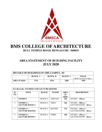
Transcription
Lecture 01 – Introduction (7/6/15)Page 01-1LECTURE 01 - INTRODUCTION TO CMOS ANALOG CIRCUITDESIGNLECTURE ORGANIZATIONOutline Introduction What is Analog Design? Skillset for Analog IC Circuit Design Trends in Analog IC Design Notation, Terminology and Symbols SummaryCMOS Analog Circuit Design, 3rd Edition ReferencePages 1-16CMOS Analog Circuit Design P.E. Allen - 2016
Lecture 01 – Introduction (7/6/15)Page 01-2INTRODUCTIONCourse ObjectiveThis course teaches analog integrated circuit design using CMOS technology.VDDVPB1I4SPECIFICATIONSI5M4I1I2I6 vINVNB1 M3 I3VPB2I7M6M1 M2M5M7VNB2M8M9M10M11vOUTCL070209-01CMOS Analog Circuit Design P.E. Allen - 2016
Lecture 01 – Introduction (7/6/15)Page 01-3Course Prerequisites Basic understanding of electronics- Active and passive components- Large and small signal models- Frequency response Circuit analysis techniques- Mesh and loop equations- Superposition, Thevenin and Norton’s equivalent circuits Integrated circuit technology- Basics process steps- PN junctionsCMOS Analog Circuit Design P.E. Allen - 2016
Lecture 01 – Introduction (7/6/15)Page 01-4Course Organization – Based on 3rd Ed. of CMOS Analog Circuit DesignAppendix ESwitched Capacitor CircuitsChapter 9D/A and A/DConvertersSystemsChapter 6Simple CMOS &BiCMOS OTA'sChapter 7High PerformanceOTA'sChapter 8CMOS/BiCMOSComparatorsComplexSimpleChapter 4CMOSSubcircuitsChapter 5CMOSAmplifiersChapterChapter102CMOS/BiCMOSD/A and MOS Analog Circuit Design070209-02 P.E. Allen - 2016
Lecture 01 – Introduction (7/6/15)Page 01-5References1.) P.E. Allen and D.R. Holberg, CMOS Analog Circuit Design – 3rd Ed., OxfordUniversity Press, 2012.2.) P.R. Gray, P.J. Hurst, S.H. Lewis and R.G. Meyer, Analysis and Design of AnalogIntegrated Circuits – 4th Ed., John Wiley and Sons, Inc., 2001.3.) B. Razavi, Design of Analog CMOS Integrated Circuits, McGraw-Hill, Inc., 2001.4.) R.J. Baker, H.W. Li and D.E. Boyce, CMOS Circuit Design, Layout, andSimulation, IEEE Press, 1998.5.) D. Johns and K. Martin, Analog Integrated Circuit Design, John Wiley and Sons,Inc., 1997.6.) K.R. Laker and W.M.C. Sansen, Design of Analog Integrated Circuits and Systems,McGraw-Hill, Inc., 1994.7.) R.L. Geiger, P.E. Allen and N.R. Strader, VLSI Techniques for Analog and DigitalCircuits, McGraw-Hill, Inc., 1990.8.) A. Hastings, The Art of Analog Layout – 2nd Ed., Prentice-Hall, Inc., 2005.9.) J. Williams, Ed., Analog Circuit Design - Art, Science, and Personalities,Butterworth-Heinemann, 1991.10.) R.A. Pease, Troubleshooting Analog Circuits, Butterworth-Heinemann, 1991.CMOS Analog Circuit Design P.E. Allen - 2016
Lecture 01 – Introduction (7/6/15)Page 01-6Course PhilosophyThis course emphasizes understanding of analog integrated circuit design.Although simulators are very powerful, the designer must understand the circuit beforeusing the computer to simulate a circuit.CMOS Analog Circuit Design P.E. Allen - 2016
Lecture 01 – Introduction (7/6/15)Page 01-7WHAT IS ANALOG DESIGN?The Analog IC Design ProcessCMOS Analog Circuit Design P.E. Allen - 2016
Lecture 01 – Introduction (7/6/15)Page 01-8What is Electrical Design?Electrical design is the process of going from the specifications to a circuit solution. Theinputs and outputs of electrical design are:LWW/L ratiosVDDCircuit orsystemsspecificationsAnalogIntegratedCircuit DesignM6M3vin M4M1CcvoutCLM2 VBias-M7M5VSSTopologyDC CurrentsFig. 1.1-3The electrical design requires active and passive device electrical models for- Creating the design- Verifying the design- Determining the robustness of the designCMOS Analog Circuit Design P.E. Allen - 2016
Lecture 01 – Introduction (7/6/15)Page 01-9Steps in Electrical Design1.) Selection of a solution- Examine previous designs- Select a solution that is simple2.) Investigate the solution- Analyze the performance (without a computer)- Determine the strengths and weaknesses of the solution3.) Modification of the solution- Use the key principles, concepts and techniques to implement- Evaluate the modifications through analysis (still no computers)4.) Verification of the solution- Use a simulator with precise models and verify thesolution- Large disagreements with the hand analysis andcomputer verification should be carefully examined.CMOS Analog Circuit Design P.E. Allen - 2016
Lecture 01 – Introduction (7/6/15)Page 01-10What is Physical Design?Physical design is the process of representing the electrical design in a layout consistingof many distinct geometrical rectangles at various levels. The layout is then used tocreate the actual, three-dimensional integrated circuit through a process calledfabrication.CIRCUITFABRICATIONLAYOUTBlue Green Black Red Orangen p 5VMetal Poly p-well n-substrateGroundvoutM2voutp M1p n p-welln-substraten nsubstrate(2.5V)M1M2vin(2.5V)White031113-015VCMOS Analog Circuit Designvin P.E. Allen - 2016
Lecture 01 – Introduction (7/6/15)Page 01-11What is the Layout Process?1.) Inputs are the W/L values and the schematic (generally from schematic entry used forsimulation).2.) A CAD tool is used to enter the various geometries. The designer must enter thelocation, shape, and level of the particular geometry.3.) During the layout, the designer must obey a set of rules called design rules. Theserules are for the purpose of ensuring the robustness and reliability of the technology.4.) Once the layout is complete, then a process called layout versus schematic (LVS) isapplied to determine if the physical layout represents the electrical schematic.5.) The next step is now that the physical dimensions of the design are known, theparasitics can be extracted. These parasitics primarily include:a.) Capacitance from a conductor to groundb.) Capacitance between conductorsc.) Bulk resistance6.) The extracted parasitics are entered into the simulated database and the design is resimulated to insure that the parasitics will not cause the design to fail.CMOS Analog Circuit Design P.E. Allen - 2016
Lecture 01 – Introduction (7/6/15)Page 01-12Packaging†Packaging of the integrated circuit is an important part of the physical design process.The function of packaging is:1.) Protect the integrated circuit2.) Power the integrated circuit3.) Cool the integrated circuit4.) Provide the electrical and mechanical connection between the integrated circuit andthe outside world.Packaging steps:Dicingthe waferAttachmentof the chip toa lead frameConnectingthe chip toa lead frameEncapsulating thechip and leadframe in a package031115-01Other considerations of packaging: Speed Parasitics (capacitive and inductive)†Rao Tummala, “Fundamentals of Microsystems Packaging,” McGraw-Hill, NY, 2001.CMOS Analog Circuit Design P.E. Allen - 2016
Lecture 01 – Introduction (7/6/15)Page 01-13What is Test Design?Test design is the process of coordinating, planning and implementing themeasurement of the analog integrated circuit performance.Objective: To compare the experimental performance with the specifications and/orsimulation results.Types of tests: Functional – verification of the nominal specifications Parametric – verification of the characteristics to within a specified tolerance Static – verification of the static (AC and DC) characteristics of a circuit or system Dynamic – verification of the dynamic (transient) characteristics of a circuit or systemAdditional Considerations:Should the testing be done at the wafer level or package level?How do you remove the influence (de-embed) of the measurement system from themeasurement?CMOS Analog Circuit Design P.E. Allen - 2016
Lecture 01 – Introduction (7/6/15)Page 01-14ANALOG INTEGRATED CIRCUIT DESIGN SKILLSETCharacteristics of Analog Integrated Circuit Design Done at the circuits level Complexity is high Continues to provide challenges as technology evolves Demands a strong understanding of the principles, concepts and techniques Good designers generally have a good physics background Must be able to make appropriate simplifications and assumptions Requires a good grasp of both modeling and technology Have a wide range of skills - breadth (analog only is rare) Be able to learn from failure Be able to use simulation correctlyCMOS Analog Circuit Design P.E. Allen - 2016
Lecture 01 – Introduction (7/6/15)Page 01-15Understanding TechnologyUnderstanding technology helps the analog IC designer to know the limits of thetechnology and the influence of the technology on the design.Device Parasitics:Connection Parasitics: 5VvinM2voutM2voutvin 5VM1M1050304-01CMOS Analog Circuit Design P.E. Allen - 2016
Lecture 01 – Introduction (7/6/15)Page 01-16Understanding ModelingModeling:Modeling is the process by which the electrical properties of an electronic circuit orsystem are represented by means of mathematical equations, circuit representations,graphs or tables.Models permit the predicting or verification of the performance of an electroniccircuit or itrepresentations,graphs, tablesPrediction orverification ofcircuit or systemperformanceElectronic Modeling Process030130-02Examples:Ohm’s law, the large signal model of a MOSFET, the I-V curves of a diode, etc.Goal:Models that are simple and allow the designer to understand the circuit performance.CMOS Analog Circuit Design P.E. Allen - 2016
Lecture 01 – Introduction (7/6/15)Page 01-17Key Principles, Concepts and Techniques of Analog IC DesignTechniques Principles mean fundamental laws that"Tricks"are precise and never change.(Webster – A comprehensive andfundamental law, doctrine, orassumption. The laws or facts of natureConcepts Analogunderlying the working of an artificialInformationIC Designthat enhancesdevice.)Processdesign Concepts will include relationships,“soft-laws” (ones that are generally true),analytical tools, things worthPrinciples (laws)remembering.040511-01used in design(Webster – An abstract idea generalizedfrom particular instances.) Techniques will include the assumptions, “tricks”, tools, methods that one uses tosimplify and understand.(Webster – The manner in which technical details are treated, a method ofaccomplishing a desired aim or goal.)CMOS Analog Circuit DesignAnalogDesign P.E. Allen - 2016
Lecture 01 – Introduction (7/6/15)Page 01-18Complexity in Analog DesignAnalog design is normally done in a non-hierarchical manner and makes little use ofrepeated blocks. As a consequence, analog design can become quite complex andchallenging.How do you handle the complexity?SystemsSystems Level (ADC)1.) Use as much hierarchy as possible.2.) Use appropriate organizationCircuits Level (op amps)techniques.3.) Document the design in an efficientCircuitsBlock Level (amplifier)manner.4.) Make use of assumptions andSub-block Level (current sink)simplifications.5.) Use simulators appropriately.ComponentsComponents (transistor)031030-03CMOS Analog Circuit Design P.E. Allen - 2016
Lecture 01 – Introduction (7/6/15)Page 01-19AssumptionsAssumptions:An assumption is taking something to be true without formal proof. Assumptions inanalog circuit design are used for simplifying the analysis or design. The goal of anassumption is to separate the essential information from the nonessentialinformation of a problem.The elements of an assumption are:1.) Formulating the assumption to simplify the problem without eliminating theessential information.2.) Application of the assumption to get a solution or result.3.) Verification that the assumption was in fact appropriate.Examples:Neglecting a large resistance in parallel with a small resistanceMiller effect to find a dominant poleFinding the roots of a second-order polynomial assuming the roots are real andseparatedCMOS Analog Circuit Design P.E. Allen - 2016
Lecture 01 – Introduction (7/6/15)Page 01-20WHERE IS ANALOG IC DESIGN TODAY?Analog IC Design has Reached MaturityThere are established fields of application: Digital-analog and analog-digital conversion Disk drive controllers Modems - filters Bandgap reference Analog phase lock loops DC-DC conversion Buffers Codecs Etc.Existing philosophy regarding analog circuits:“If it can be done economically by digital, don’t use analog.”Consequently:Analog finds applications where speed, area, or power have advantages over adigital approach.CMOS Analog Circuit Design P.E. Allen - 2016
Lecture 01 – Introduction (7/6/15)Page 01-21Analog IC Design ChallengesTechnology: Digital circuits have scaled well with technology Analog does not benefit as much from smaller features- Speed increases- Gain decreases- Matching decreases- Nonlinearity increases- New issues appear such as gate current leakageAnalog Circuit Challenges: Trade offs are necessary between linearity, speed, precision and power As analog is combined with more digital, substrate interference will become worseCMOS Analog Circuit Design P.E. Allen - 2016
Lecture 01 – Introduction (7/6/15)Digitally Assisted Analog CircuitsUse digital circuits which work better atscaled technologies to improve analogcircuits that do not necessarily improvewith technology scaling.Principles and Techniques: Open-loop vs. closed loop- Open loop is less accurate but smaller - Closed-loop is more accurate but larger Page 01-22Faster, less powerSlower, more power Averaging- Increase of accuracy Smaller devices, more speed Calibration- Accuracy increases Increased resolution with same area Dynamic Element Matching- Enhancement of component precision Doubly correlated sampling- Reduction of dc influences (noise, offset) Smaller devices, more speed Etc.CMOS Analog Circuit Design P.E. Allen - 2016
Lecture 01 – Introduction (7/6/15)Page 01-23A New Paradigm for IC Design? Today’s Paradigm– invested up front– No guarantee that product will be profitable– Requires a lot of overhead, support, and timePotential market foran IC is identifiedIC is designed andfabricatedIC ismarketed150623-02 New Paradigm (shaped by the internet)––––––No invested until the product is soldThe need for an IC is generated by potential consumerOpens the design space to a wide range of “designers”Massive markets not needed to make a product and profitMinimizes the time and overhead required to develop a productDesign equivalent of crowd funding “crowd designing”CMOS Analog Circuit Design P.E. Allen - 2016
Lecture 01 – Introduction (7/6/15)Page 01-24NOTATION, TERMINOLOGY AND SYMBOLOGYDefinition of Symbols for Various SignalsSignal DefinitionTotal instantaneous value of the DC value of the signalAC value of the lex variable, phasor, or rms value Uppercaseof the signalLowercaseQaDrain CurrentExample:idIDIdmiDtFig. 1.4-1CMOS Analog Circuit Design P.E. Allen - 2016
Lecture 01 – Introduction (7/6/15)Page 01-25MOS Transistor SymbolsDEnhancementNMOS withVBS 0V.GEnhancementPMOS withVBS 0V.GSDDSEnhancementB NMOS withVBS ¹ 0V.GEnhancementB PMOS withVBS ¹ 0V.GSDDSSimpleNMOSsymbolGSCMOS Analog Circuit DesignSSimplePMOSsymbolGD P.E. Allen - 2016
Lecture 01 – Introduction (7/6/15)Page 01-26Other Schematic Symbols V--Differential amplifier,op amp, or comparator AvV1 -V1I1VV- -Independentvoltage sources V2V1--Voltage-controlled,voltage sourceIndependentcurrent sourceI2GmV1I1Voltage-controlled,current sourceI2 RmI1 -V2AiI1Current-controlled,voltage sourceCMOS Analog Circuit DesignCurrent-controlled,current source P.E. Allen - 2016
Lecture 01 – Introduction (7/6/15)Page 01-27Three-Terminal NotationQABCA Terminal with the larger magnitude of potentialB Terminal with the smaller magnitude of potentialC Condition of the remaining terminal with respect to terminal BC 0 There is an infinite resistance between terminal B and the 3rd terminalC S There is a zero resistance between terminal B and the 3rd terminalC R There is a finite resistance between terminal B and the 3rd terminalC X There is a voltage source in series with a resistor between terminal Band the 3rd terminal in such a manner as to reverse bias a PNjunction.IDSSSSDDExamples-VGSCDGS G(a.)G DIDSS(b.)BVDGOG-(c.)(a.) Capacitance from drain to gate with the source shorted to the gate.(b.) Drain-source current when gate is shorted to source (depletion device)(c.) Breakdown voltage from drain to gate with the source is open- circuited to the gate.CMOS Analog Circuit Design P.E. Allen - 2016
Lecture 01 – Introduction (7/6/15)Page 01-28SUMMARY Successful analog IC design proceeds with understanding the circuit before simulation. Analog IC design consists of three major steps:1.) Electrical design Topology, W/L values, component values and dc currents2.) Physical design (Layout)3.) Test design (Testing) Analog designers must be flexible and have a skill set that allows one to simplify andunderstand a complex problem Analog IC design has reached maturity and is here to stay. The appropriate philosophy is “If it can be done economically by digital, don’t useanalog”. As a result of the above, analog finds applications where speed, area, or power result inadvantages over a digital approach. Deep-submicron technologies will offer exciting challenges to the creativity of theanalog designer. Paradigm for IC design might be changing which would influence analog IC design.CMOS Analog Circuit Design P.E. Allen - 2016
Electrical design is the process of going from the specifications to a circuit solution. The inputs and outputs of electrical design are: The electrical design requires active and passive device electrical models for - Creating the design - Verifying the design - Determining the robustness of the design - v in M1 M2 M3 M4 M5 M6 M7 v out V DD V .