Transcription
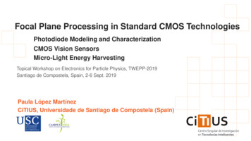
Focal Plane Processing in Standard CMOS TechnologiesPhotodiode Modeling and CharacterizationCMOS Vision SensorsMicro-Light Energy HarvestingTopical Workshop on Electronics for Particle Physics, TWEPP-2019Santiago de Compostela, Spain, 2-6 Sept. 2019Paula López MartínezCiTIUS, Universidade de Santiago de Compostela (Spain)
Outline Vision – Analog to Information Conversion (AIC) by means of focal planeprocessing in standard CMOS technologies. Mission - Change of paradigm from big data to smart data.Development of new solutions extracting information from the environment ratherthan simply massive amounts of raw data, efficiently reducing bandwidth andpower consumption. The use of standard CMOS technologies favors thedevelopment of low cost solutions.Vertical approach: from sensing to processing to energy autonomy2
Photodiode Modeling andCharacterization3
Goal – Determination of the practical scaling limit of photodiodes in standardCMOS technologies Modeling and experimental characterization under point source illumination sub-pixel level study Modeling and experimental characterization under uniform illumination4
Point Source IlluminationNorth, south, eastand west neighbors’pixel electronicsDUT1D analytical model vs experimental resultsSurroundings Array of 4um x 8um 3T-APS pixels inchessboard configuration P-N and P-Nwell photodiodes UMC 90 nm standard CMOS technologyActive areaSurroundingsLateraldepletion areas5
Uniform illumination Goal – Determination of the relative importance of the lateral collection withrespect to the active area collection. Development of a 2D, compact, general and scalable model for P-N [1,2] and PNwell [3] PDs Experimental validation: square P-N junctions in AMS 180 nm and UMC 65 nmstandard CMOS technologies [4] Verilog-AMS implementation [5][1] Solid-State Electronics, vol. 73, pp. 15–20, Jul. 2012[2] IEEE Transactions on electron devices, VOL. 60, NO. 10, pp. 3459-3464, 2013[3] IEEE Transactions on electron devices, VOL. 62, NO. 2, pp. 580-586, 2015[4] Semicond. Sci. Technol., vol. 28, no. 4, pp. 045011–045017, 2013[5] Microelectronics Journal 43 (2012) 980–9846
Uniform illumination Fabricated structures:Metal layers7
Uniform illuminationExperimental resultsLateral component dominatesthe total photocurrent!!8
Uniform illumination 2D model:9
CMOS Vision Sensor for GaussianPyramid10
Feature Detectors on CMOS Vision Sensors CMOS vision sensor (CVIS) chips Embedded parallel processing close to the sensors Per-column or per-pixel processors (or both of them combined)̶ Advantages Fast and power efficient image analysis̶ Drawbacks Larger pixel pitch with smaller fill-factor than imagers Low resolution11
CMOS Vision Sensors: Gaussian pyramid Goal- design of a CMOS Vision Sensor (CVIS) chip for Gaussian pyramidextraction1 Gaussian Pyramid Extraction- first stage of many feature detectors; itprovides algorithms with scale invariance Applications- tracking, object detection, image registration, etc.[1] IEEE J. of Solid-State Circuits, vol. 52, no. 2, pp. 483-495, 201712
CMOS Vision Sensor for Gaussian Pyramid Gaussian pyramid emulates the lost of high spatial frequency componentsas an object moves away from the camera Organized in octaves(downscaling theprevious one in 1/4x) Each octave with 6images or scales A scale is aGaussian filter with agiven sigma level onthe incoming imageBreakdown of SIFTalgorithm (@ HD, @30fps, @ #3375 keypoints) 3 octaves with 6scales each sufficeGaussianpyramid92%13
CMOS Vision Sensor for Gaussian Pyramid- chip features 176 x 120 pixels (5 x 5 mm2) in standard 180 nm CMOS technology 88 x 60 Processing Elements (PE) for close to the sensor and concurrentprocessing Every PE occupies 44 x 44 µm2, comprising: 4 nwell/psub photodiodes of 8 x 8 µm2 in 3T-APS configuration 4 state and 4 exchange capacitors Circuits for in-PE ADC and CDS̶ Hardware reuse Read-out with an 8-bit single-slope ADC14
CMOS Vision Sensor for Gaussian Pyramid- chip features- pixelschematicsSwitched-CapacitorNetwork- More linear thanresistor-basedsolutions- Better control of σthrough thenumber of clockcycles15
CMOS Vision Sensor for Gaussian PyramidExperimental Results Test Setup16
CMOS Vision Sensor for Gaussian PyramidExperimental Results Input image and different snapshots ofthe on-chip Gaussian pyramid for σ 1.77 (number of clock cycles of thedouble-Euler, n 19), σ 2.17 (n 29),and σ 2.51 (n 39) Accuracy assessment:Sigma : Theoretical (black); Experimental (blue)RMSE- comparison with the Gaussian filter withnumerical simulations (Matlab).17
CMOS Vision Sensor for Gaussian PyramidExperimental Results: comparison with conventional solutionsHW SolutionFunctionEnergy/frameEnergy/pxMpx/sThis work180 nm CMOSGaussianPyramid176 x 120 px70 mW @ 8 ms0.56 mJ/frame26.5 nJ/px2.64Ref. [1] OV9655 Core-i7GaussianPyramidVGA resolution90 mW @ 30 fps 35 W @ 136 ms4.8 J/frame15.5 uJ/px2.26Ref. [2] OV9655 Core-2-DuoGaussianPyramidVGA resolution90 mW @ 30 fps 35 W @ 2.1 s73.7 J/frame240 uJ/px0.15Ref. [3] OV9622 QualcommSnapdragon S4GaussianPyramid350 x 256 px30 mW 4 W @ 98.5 ms0.4 J/frame4.4 uJ/px0.91[1] M. Murphy et al., “Image Feature Extraction for Mobile Processors”, IEEE IIWSC 2009[2] Feng-Cheng Huang et al., “High-Performance SIFT Hardware Accelerator for Real-Time ImageFeature Extraction”, IEEE TCAS-VT, vol. 22, no. 2, March 2012[3] G. Wang et al., “Workload Analysis and Efficient OpenCL-based Implementation of SIFTAlgorithm on a Smartphone”, IEEE GlobalSIP 201318
CMOS Vision Sensor for BackgroundSubtraction19
CMOS Vision Sensor for Background Subtraction Hardware-Oriented Pixel Based Adaptive Segmenter (HO-PBAS)- D. García-Lesta et al., “In-PixelAnalog Memories for a Pixel-Based Background Subtraction Algorithm on CMOS Vision Sensors”, Int. J. of Circuit Theory andApplications, 201820
CMOS Vision Sensor for Background Subtraction Pixel Architecture[1] D. Lesta et al., International Journal of Circuit Theory and Applications, pp. 1631-1647 , 2018.21
CMOS Vision Sensor for Background Subtraction Scalable analog core Column parallel single-slope 8-bits ADC Ncol x 8 bits row buffer that holds a rowconversion while the next one is beingconverted Global control22
CMOS Vision Sensor for Background SubtractionARAM Analog memories Open-loop architecture with SF asoutput buffers [1] MIM capacitors Non-destructive readings Write error- 3 mV Voltage drift- 1mV/sThe same transformation isapplied to the incoming valuefrom the 3T APS to minimize theimpact[1] D. Lesta et al., International Journal of Circuit Theory and Applications, pp. 1631-1647 , 2018.23
CMOS Vision Sensor for Background SubtractionLayouts24
CMOS Vision Sensor for Background SubtractionLayouts25
On-chip Micro Energy Harvesting26
Micro-Energy Harvesting Chip FeaturesChip - Energy HarvestingFeaturesEnergy transducer and PMUBoth of them on-chipTechnologyStandard 0.18 um CMOS (UMC)AreaPhotodiode- 1 mm2, PMU- 0.575mm2Voltage boostingCapacitive DC-DC converterprogramable Dickson topologygain, fly capacitors and frequencyStart-upCold- no external mechanismsEnergy span2.38 nW- 10 uWMPPTOpen-loop- different workingregions (WR) according to thephotodiode voltage; VPD27
Micro-Energy Harvesting Chip Architecture28
Micro-Energy Harvesting Chip Architecture MPPT Open-loop Continuous and bidimensionalchanges in topology, fly capacitorsand frequency of the main chargepump (Dickson) 5 working regions (WR) according toillumination levels (VPD) Maximum current for a given outputvoltage, in this case 1.1 V Voltage levels of WR defined duringthe design phase with a joint modelof photodiode and Dickson chargepump [1][1] E. Ferro, P. López, V.M. Brea, D. Cabello. “Dynamic joint model of capacitive charge pumpsand on-chip photovoltaic cells for CMOS micro-energy harvesting”. Int. J. of Circuit Theory andApplications, vol. 44, no. 10, pp. 1874-1894, 2016.29
Micro-Energy Harvesting Chip Architecture30
Micro-Energy Harvesting Chip Architecture31
Micro-Energy Harvesting Chip Architecture32
Micro-Energy Harvesting Chip Architecture33
Proof-of-Concept Chip- Power Breakdown (Simulation)34
Proof-of-Concept Chip- Test Structure35
Proof-of-Concept Chip- Experimental Set-Up36
Proof-of-Concept Chip- Experimental Results- Working Regions (WR’s) Expected voltage levels (WR thresholds)- 0.25 V, 0.31 V, 0.37 V, 0.42 V Measured voltage levels (WR thresholds)- 0.258 V, 0.316 V, 0.40 V, 0.44 V37
Proof-of-Concept Chip- Experimental Results- Cold Start-Up Results with an off-chip 100 nF Ta capacitor Start-up power- 2.38 nW38
Proof-of-Concept Chip- Experimental Results- End-to-End Efficiency39
Proof-of-Concept Chip- State-of-the-Art Comparison40
Proof-of-Concept Chip- Off-the-Shelf PMU’s ComparisonOur ChipBQ25570Texas Inst.March 2015BQ25504Texas Inst.June 2015SizeOn-chip solar celland PMU 1.6 mm2PMU3.5 mm x 3.5 mmPMU3.5 mm x 3.5 mmStart-Upcurrent 5 nA(9.52 nA x 0.25 V)15 uW(60.000 nA x 0.25 V)15 uW(60.000 nA x 0.25 V)Off-chipcomponentsNoInductors andresistorsInductors andresistorsBias currentnA448 nA330 nA41
Conclusions and Outlook Past and on-going work Device modeling and experimental characterization Focal-Plane Processing, in standard CMOS technologies for conventionalComputer Vision algorithms Light micro-energy harvesting in standard CMOS technologies for implantable,wearable or IoT devices Future work- MENELAOSNT (ETN- 2020- 2023, European Funding),ENVISAGE (2019- 2021, Spanish Funding) Time-of-flight sensors (standard CMOS technologies) CMOS vision sensors incorporating deep learning techniques Light micro-energy harvesting in standard CMOS technologiesMenelaos NTMultimodal Environmental Exploration Systemshttp://www.menelaos-nt.eu/Novel Technologies44
Thanks for your attention!Fondo Europeo de Desenvolvemento Rexional “Unha maneira de facer Europa”45
CMOS Vision Sensor for Gaussian Pyramid- chip features 14 176 x 120 pixels (5 x 5 mm2) in standard 180 nm CMOS technology 88 x 60 Processing Elements (PE) for close to the sensor and concurrent processing Every PE occupies 44 x 44 µm2, comprising: 4 nwell/psub photodiodes of 8 x 8 µm2 in 3T-APS configuration 4 state and 4 exchange capacitors Circuits for in-PE ADC and CDS ̶Hardware reuse .