Transcription
Introduction toCMOS VLSIDesignLecture 4:CMOS Transistor TheoryDavid Harris, Harvey Mudd CollegeKartik Mohanram and Steven LevitanUniversity of Pittsburgh
OutlineqqqqqqqIntroductionMOS CapacitornMOS I-V CharacteristicspMOS I-V CharacteristicsGate and Diffusion CapacitancePass TransistorsRC Delay Models3: CMOS Transistor TheoryCMOS VLSI DesignSlide 2
Introductionq So far, we have treated transistors as ideal switchesq An ON transistor passes a finite amount of current– Depends on terminal voltages– Derive current-voltage (I-V) relationshipsq Transistor gate, source, drain all have capacitance– I C (ΔV/Δt) - Δt (C/I) ΔV– Capacitance and current determine speedq Also explore what a “degraded level” really means3: CMOS Transistor TheoryCMOS VLSI DesignSlide 3
MOS Transistors - Types and SymbolsDDGGSSNMOS Enhancement NMOS DepletionDGGSPMOS Enhancement Digital Integrated Circuits2ndDBSNMOS withBulk ContactDevices
The MOS TransistorPolysilicon Digital Integrated Circuits2ndAluminumDevices
Controlling current flow in an nFET. Digital Integrated Circuits2ndIntroduction to Circuits, Fourth Edition by Peter Uyemura,DevicesCopyright 2004 John Wiley & Sons. All rights reserved.
Controlling current flow in a pFET. Digital Integrated Circuits2ndIntroduction to Circuits, Fourth Edition by Peter Uyemura,DevicesCopyright 2004 John Wiley & Sons. All rights reserved.
What is a Transistor?A Switch!A MOS TransistorVGS V TS Digital Integrated Circuits2nd VGS R onDDevices
I-V CurvesCurrent (I) vs. Voltage (V)I f(V)-46x 105ID (A)432100ResistorI V/RDiodeI Is*exp(k*V-Vt)0.51VDS1.52MOSI f(Vgs, Vds)2.5
Terminal VoltagesVgq Mode of operation depends on Vg, Vd, Vs – Vgs Vg – VsVgsVgd– Vgd Vg – VdVsVd– Vds Vd – Vs Vgs - Vgd Vdsq Source and drain are symmetric diffusion terminals– By convention, source is terminal at lower voltage– Hence Vds 0q nMOS body is grounded. First assume source is 0 too.q Three regions of operation– Cutoff– Linear– Saturation3: CMOS Transistor TheoryCMOS VLSI DesignSlide 10
MOS Capacitorq Gate and body form MOS capacitorq Operating modes– Accumulation– Depletion– InversionVg 0 -polysilicon gatesilicon dioxide insulatorp-type body(a)0 Vg V tIn general, MOSgate capacitanceis not constant -depletion region(b)Vg V t -inversion regiondepletion region(c)3: CMOS Transistor TheoryCMOS VLSI DesignSlide 11
MOS Transistors – Operating regions2nd Digital IntegratedCopyright 2005 CircuitsPearson Addison-Wesley. All rights reserved.Devices
nMOS Cutoffq No channelq Ids 0dVgs 0 -gsg3: CMOS Transistor TheoryVgddn s n p-type bodybCMOS VLSI DesignSlide 13
nMOS Linearq Channel formsq Current flows from d to sV– e from s to dq Ids increases with Vdsq Similar to linear resistorgs Vt -sVgd VgsVds 0n p-type bodybVgs Vt -gss dn dgg dn n Vgs Vgd VtIds0 Vds Vgs-Vtp-type bodyb3: CMOS Transistor TheoryCMOS VLSI DesignSlide 14
Linear Region Vgs Vt & Vgd VtSVGSVDSGn – V(x)IDDIdsn S transistorbias conditionsChannel exists, Current Flowssince Vds 0Ids k’(W/L)((Vgs-Vt)Vds-Vds2/2) Digital Integrated Circuits2ndIdsI V/RR 1/(k’(W/L)(Vgs-Vt))VdsDevices
nMOS SaturationqqqqChannel pinches offIds independent of VdsWe say current saturatesSimilar to current sourcedgVgs Vt -gVgd Vtd Idsss -n n Vds Vgs-Vtp-type bodyb3: CMOS Transistor TheoryCMOS VLSI DesignSlide 16
Saturation: Vgs Vt & Vgd VtVGSIdsVDS VGS - VTGDSn -VGS - VT n VgdIdsVgsPositive Charge on Gate:Channel exists, Current Flowssince Vds 0But: channel is “pinched off”Ids (k’/2)(W/L)(Vgs-Vt)2 Digital Integrated Circuits2ndDevices
I-V Characteristicsq In Linear region, Ids depends on– How much charge is in the channel?– How fast is the charge moving?3: CMOS Transistor TheoryCMOS VLSI DesignSlide 18
MOS Transistors – Regions Transitions2nd Digital IntegratedCopyright 2005 CircuitsPearson Addison-Wesley. All rights reserved.Devices
Channel Chargeq MOS structure looks like parallel plate capacitorwhile operating in inversion– Gate – oxide – channelq Qchannel gateVgpolysilicongateWtoxn Ln SiO2 gate oxide(good insulator, εox 3.9) Cg Vgd drainsource VgsVsVdchannel n n Vdsp-type bodyp-type body3: CMOS Transistor TheoryCMOS VLSI DesignSlide 20
Channel Chargeq MOS structure looks like parallel plate capacitorwhile operating in inversion– Gate – oxide – channelq Qchannel CVq C gateVgpolysilicongateWtoxn Ln SiO2 gate oxide(good insulator, εox 3.9) Cg Vgd drainsource VgsVsVdchannel n n Vdsp-type bodyp-type body3: CMOS Transistor TheoryCMOS VLSI DesignSlide 21
Channel Chargeq MOS structure looks like parallel plate capacitorwhile operating in inversion– Gate – oxide – channelq Qchannel CVq C Cg εoxWL/tox CoxWLCox εox / toxCox 8.6*fF/um2q V gateVgpolysilicongateWtoxn Ln SiO2 gate oxide(good insulator, εox 3.9) Cg Vgd drainsource VgsVsVdchannel n n Vdsp-type bodyp-type body3: CMOS Transistor TheoryCMOS VLSI DesignSlide 22
Channel Chargeq MOS structure looks like parallel plate capacitorwhile operating in inversion– Gate – oxide – channelq Qchannel CVq C Cg εoxWL/tox CoxWLCox εox / toxq V Vgc – Vt (Vgs – Vds/2) – VtgateVgpolysilicongateWtoxn Ln SiO2 gate oxide(good insulator, εox 3.9) Cg Vgd drainsource VgsVsVdchannel n n Vdsp-type bodyp-type body3: CMOS Transistor TheoryCMOS VLSI DesignSlide 23
Carrier velocityq Charge is carried by eq Carrier velocity v proportional to lateral E-fieldbetween source and drainq v 3: CMOS Transistor TheoryCMOS VLSI DesignSlide 24
Carrier velocityq Charge is carried by eq Carrier velocity v proportional to lateral E-fieldbetween source and drainq v µEµ called mobilityq E 3: CMOS Transistor TheoryCMOS VLSI DesignSlide 25
Carrier velocityq Charge is carried by eq Carrier velocity v proportional to lateral E-fieldbetween source and drainq v µEµ called mobilityq E Vds/Lq Time for carrier to cross channel:– t 3: CMOS Transistor TheoryCMOS VLSI DesignSlide 26
Carrier velocityq Charge is carried by eq Carrier velocity v proportional to lateral E-fieldbetween source and drainq v µEµ called mobilityq E Vds/Lq Time for carrier to cross channel:– t L/v3: CMOS Transistor TheoryCMOS VLSI DesignSlide 27
nMOS Linear I-Vq Now we know– How much charge Qchannel is in the channel– How much time t each carrier takes to crossI ds 3: CMOS Transistor TheoryCMOS VLSI DesignSlide 28
nMOS Linear I-Vq Now we know– How much charge Qchannel is in the channel– How much time t each carrier takes to crossQchannelI ds t 3: CMOS Transistor TheoryCMOS VLSI DesignSlide 29
nMOS Linear I-Vq Now we know– How much charge Qchannel is in the channel– How much time t each carrier takes to crossQchannelI ds tW µCoxL V V Vds gs t2 V β Vgs Vt ds Vds2 3: CMOS Transistor Theory V ds CMOS VLSI DesignWβ µCoxLSlide 30
Computed CurvesLinear ResistorVgs 5vVgs 4.5vVgs 4.0v Digital Integrated Circuits2ndDevices
nMOS Saturation I-Vq If Vgd Vt, channel pinches off near drain– When Vds Vdsat Vgs – Vtq Now drain voltage no longer increases currentI ds 3: CMOS Transistor TheoryCMOS VLSI DesignSlide 32
nMOS Saturation I-Vq If Vgd Vt, channel pinches off near drain– When Vds Vdsat Vgs – Vtq Now drain voltage no longer increases currentVdsat I ds β Vgs Vt 2 3: CMOS Transistor Theory V dsat CMOS VLSI DesignSlide 33
nMOS Saturation I-Vq If Vgd Vt, channel pinches off near drain– When Vds Vdsat Vgs – Vtq Now drain voltage no longer increases currentVI ds β Vgs Vt dsat2 βV(2gs Vt )3: CMOS Transistor Theory V dsat 2CMOS VLSI DesignSlide 34
Computed CurvesLinear ResistorVgs 5vVgs 4.5vVgs 4.0v3: CMOS Transistor TheoryCMOS VLSI DesignSlide 35
nMOS I-V Summaryq Shockley 1st order transistor models 0 VdsI ds β Vgs Vt 2 2β Vgs Vt )( 23: CMOS Transistor TheoryVgs Vt V V V dsdsdsat Vds VdsatCMOS VLSI DesigncutofflinearsaturationSlide 36
Exampleq We will be using a 0.180 µm process for your project– From TSMC Semiconductor– tox 40 Å– µ 180 cm2/V*s– Vt 0.4 Vq Plot Ids vs. Vds– Vgs 0, 0.3, , 1.8– Use W/L 4/2 λ 3.9 8.85 10 14 W WW155β µCox (180350) 120µ A /V 2 8LL40 10 100 L 3: CMOS Transistor TheoryCMOS VLSI DesignSlide 37
pMOS I-Vq All dopings and voltages areinverted for pMOSq Mobility µp is determined byholes– Typically 2-3x lower thanthat of electrons µnq Thus pMOS must be wider toprovide same current– Often, assume µn / µp 23: CMOS Transistor TheoryCMOS VLSI DesignSlide 38
Current-Voltage RelationsLong-Channel DeviceCut-off (VGS – VT 0) “no current” (not really) Digital Integrated Circuits2ndDevices
ID versus VDS short channel device-46-4x 10VGS 2.5 Vx 102.5VGS 2.5 V52Resistive SaturationID (A)VGS 2.0 V3VDS VGS - VT21.51VGS 1.5 V0.5VGS 1.0 VVGS 1.5 V100VGS 2.0 VID (A)4VGS 1.0 V0.51VDS(V)1.5Long Channel Digital Integrated Circuits2nd22.5000.51VDS(V)1.52Short ChannelDevices2.5
Rabaey’s unified modelfor manual analysisGSDB Digital Integrated Circuits2ndDevices
Transistor Modelfor Manual Analysis Digital Integrated Circuits2ndDevices
Simple Model versus SPICE2.5x 10-4VDS VDSAT2VelocitySaturatedID (A)1.5Linear1VDSAT VGT0.5VDS VGT000.5Saturated11.522.5VDS (V) Digital Integrated Circuits2ndDevices
Even Simpler:The Transistor as a SwitchVGS V TSR onIDV GS VD DDRmidR0V DSVDD/2 Digital Integrated Circuits2ndVDDDevices
The Transistor as a SwitchThis week’s Lab – find Req for our TSMC 180nm process Digital Integrated Circuits2ndDevices
Saturation EffectsDischarge of 1pf capacitor, with Vgs of 3,4,5 volts. Also, 12k resistor.dgWhich is the resistor?s Digital Integrated Circuits2ndDevices
More on Capacitanceq Any two conductors separated by an insulator havecapacitanceq Gate to channel capacitor is very important– Creates channel charge necessary for operationq Source and drain have capacitance to body– Across reverse-biased diodes– Called diffusion capacitance because it isassociated with source/drain diffusion3: CMOS Transistor TheoryCMOS VLSI DesignSlide 47
Gate Capacitanceq Approximate channel as connected to sourceq Cgs εoxWL/tox CoxWL CpermicronWq Cpermicron is typically about 2 fF/µmpolysilicongateWtoxn Ln SiO2 gate oxide(good insulator, εox 3.9ε0)p-type body3: CMOS Transistor TheoryCMOS VLSI DesignSlide 48
The Gate CapacitancePolysilicon gateSourcexdn xdLdWDrainn Gate-bulkoverlapTop viewGate oxidetoxn Ln Cross section Digital Integrated Circuits2ndDevices
Dynamic Behavior of MOS TransistorGCGSCGDDSCGBCSBCDBB Digital Integrated Circuits2ndDevices
Physical visualization of FETcapacitances Digital Integrated Circuits2ndIntroduction to Circuits, Fourth Edition by Peter Uyemura,DevicesCopyright 2004 John Wiley & Sons. All rights reserved.
MOS Capacitances Behavior !2nd Digital IntegratedCopyright 2005 CircuitsPearson Addison-Wesley. All rights reserved.Devices
Gate Capacitance – onMost important regions in digital design: saturation and cut-off Digital Integrated Circuits2ndDevices
Measuring the Gate Cap109Gate Capacitance (F)V GSI3 102 1687654322 2 2 1.5 2 1 2 0.5 0 0.5V GS (V) Digital Integrated Circuits2nd11.52Devices
Diffusion Capacitanceq Csb, Cdbq Undesirable, called parasitic capacitanceq Capacitance depends on area and perimeter– Use small diffusion nodes– Comparable to Cgfor contacted diff– ½ Cg for uncontacted– Varies with process3: CMOS Transistor TheoryCMOS VLSI DesignSlide 55
Diffusion CapacitanceChannel-stop implantNA1Side wallSourceNDWBottomxjSide wallLS Digital Integrated Circuits2ndChannelSubstrateN ADevices
Calculation of the FET junctioncapacitance Digital Integrated Circuits2ndIntroduction to Circuits, Fourth Edition by Peter Uyemura,DevicesCopyright 2004 John Wiley & Sons. All rights reserved.
Capacitances in 0.25 µm CMOSprocessValues for a Typical Device: Digital Integrated Circuits2ndDevices
Parasitic ResistancesPolysilicon gateLDGDraincontactDSRSWVGS,effRDDrain Digital Integrated Circuits2ndDevices
Final construction of the nFET RCmodelCG Digital Integrated Circuits2ndIntroduction to Circuits, Fourth Edition by Peter Uyemura,DevicesCopyright 2004 John Wiley & Sons. All rights reserved.
LatchupVDD p nn pp-sourceRnwellp-substrate(a) Origin of latchup Digital Integrated Circuits2ndRnwelln pn-wellRpsubs VD Dn-sourceRpsubs(b) Equivalent circuitDevices
Summary of MOSFET OperatingRegionsq StrongInversion VGS VT§ Linear (Resistive) VDS VDSAT§ Saturated (Constant Current) VDS VDSATq WeakInversion (Sub-Threshold) VGS VT§ Exponential in VGS with linear VDS dependence Digital Integrated Circuits2ndDevices
SPICE MODELSLevel 1: Long Channel Equations - Very SimpleLevel 2: Physical Model - Includes VelocitySaturation and Threshold VariationsLevel 3: Semi-Emperical - Based on curve fittingto measured devicesLevel 4 (BSIM): Emperical - Simple and Popular Digital Integrated Circuits2ndDevices
Main MOS SPICE Parameters Digital Integrated Circuits2ndDevices
SPICE Parameters for Parasitics Digital Integrated Circuits2ndDevices
SPICE Transistors Parameters Digital Integrated Circuits2ndDevices
Circuit Simulation Model of CMOS Inverter Digital Integrated Circuits2ndDevices
Pass Transistorsq Wehave assumed source is groundedVDDq What if source 0?VDD§ e.g. pass transistor passing VDD3:IntegratedCMOSCircuitsTransistor2nd DigitalTheorySlide 68Devices
Pass TransistorsqqWe have assumed source is groundedWhat if source 0?§ e.g. pass transistor passing VDDqVDDVDDVg VDD§ If Vs VDD-Vt, Vgs Vt§ Hence transistor would turn itself offqnMOS pass transistors pull no higher than VDD-Vtn§ Called a degraded “1”§ Approach degraded value slowly (low Ids)qpMOS pass transistors pull no lower than Vtp3:IntegratedCMOSCircuitsTransistor2nd DigitalTheorySlide 69Devices
Pass Transistor cuitsTransistor2nd DigitalTheorySlide 70Devices
Pass Transistor CktsVDDVDDVDDVs VDD-VtnVDDVDDVDD-Vtn VDD-VtnVDDVs Vtp Transistor2nd DigitalVDDVDD-2VtnSlide 71Devices
Effective ResistanceqShockley models have limited value§ Not accurate enough for modern transistors§ Too complicated for much hand analysisqSimplification: treat transistor as resistor§ Replace Ids(Vds, Vgs) with effective resistance R– Ids Vds/R§ R averaged across switching of digital gateqToo inaccurate to predict current at any given time§ But good enough to predict RC delay3:IntegratedCMOSCircuitsTransistor2nd DigitalTheorySlide 72Devices
RC Delay ModelqUse equivalent circuits for MOS transistors§ Ideal switch capacitance and ON resistance§ Unit nMOS has resistance R, capacitance C§ Unit pMOS has resistance 2R, capacitance CqqCapacitance proportional to widthResistance inversely proportional to ransistor2nd Digitaldks2R/kgkCkCdTheorySlide 73Devices
RC ValuesqCapacitance§ C Cg Cs Cd 2 fF/µm of gate width§ Values similar across many processesqResistance§ R 6 KΩ*µm in 0.6um process§ Improves with shorter channel lengthsqUnit transistors§ May refer to minimum contacted device (4/2 λ)§ Or maybe 1 µm wide device§ Doesn’t matter as long as you are consistent3:IntegratedCMOSCircuitsTransistor2nd DigitalTheorySlide 74Devices
Inverter Delay Estimateq Estimatethe delay of a fanout-of-1inverterA2 Y2113:IntegratedCMOSCircuitsTransistor2nd DigitalTheorySlide 75Devices
Inverter Delay Estimateq EstimateinverterA2 Y211the cuitsTransistor2nd DigitalTheorySlide 76Devices
Inverter Delay Estimateq EstimateinverterA2 Y211the CMOSCircuitsTransistor2nd DigitalTheorySlide 77Devices
Inverter Delay Estimateq EstimateinverterA2 Y211the delayofafanout-of-12CR2C2CYRCC2CRC2CCCd 6RC3:IntegratedCMOSCircuitsTransistor2nd DigitalTheorySlide 78Devices
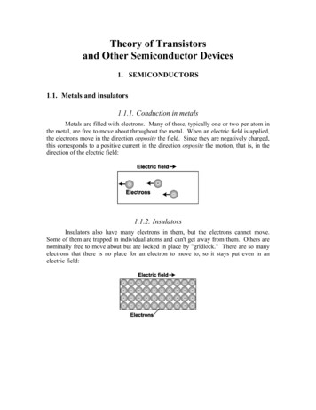
3: CMOS Transistor Theory CMOS VLSI Design Slide 3 Introduction q So far, we have treated transistors as ideal swit