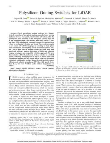
Transcription
Arrayed Waveguide GratingDr. Martin AmersfoortConcept to Volume b.v.15 June 1998Application note A1998003C2VTel: 31 534 889 889Fax: 31 534 889 890software@c2v.nlwww.c2v.nl
Table of ContentsARRAYED WAVEGUIDE GRATINGiiI1.Introduction12.General AWG design33.BPM Simulation104.Layout and simulation example135.Implementation details176.References21
AbstractAbstractThis application note requires the basic and advanced mode solvermodules in the Selene/Cross-section interface, and the BPM and masklayout modules in the Prometheus/Topview interface.This application note describes how to design, simulate and layout anArrayed Waveguide Grating (AWG) using OlympIOs.The operation principle of the AWG is described and additionallysome simple design rules are given.We have described how to simulate the AWG by means of BeamPropagation Methods (BPM), by breaking it into three sections: aninput star, an array of decoupled waveguides and an output star. Asimulation example is presented which shows that the relevantparameters related to the AWG’s spectral response can be obtainedusing this method. Moreover, they agree quite well with the designvalues.Finally, we have provided the details concerning the implementation ofthese designs into OlympIOs, using the hierarchical design featuresincorporated in this package.C2V A19980031
www.c2v.nl1. IntroductionIn recent years Arrayed Waveguide Gratings ([Smit88], avelength(de)multiplexers for WDM applications. They have proven to becapable of precise demultiplexing of a large number of channels withrelative low lossses.This application note describes how to design and simulate an ArrayedWaveguide Grating (AWG) using OlympIOs. The contents of thisnote are as follows.General AWG design, page 3, outlines the operation principle of theAWG and in addition gives some simple design rules for thiscomponent. BPM Simulation, page 10, describes the simulation of theAWG using the Beam Propagation Method (BPM). Layout andsimulation example, page 13, describes the results of a design andsimulation of an example design. Implementation details, page 17,describes some tips with respect to the implementation of the AWGdesign into OlympIOs.2helpdesk@c2v.nl
General AWG design2. General AWG designThis chapter describes the basic operation principles of the AWG (alsoknown as the optical phased-array), how to calculate the basicproperties such as dispersion, and provides some simple design rulesfor optimum performance.2.1. Operation principleFigure 1 shows a schematic representation of the phased-arraydemultiplexer. The device consist of two slab waveguide star couplers,connected by a dispersive waveguide array. The operation principle isas follows. Light propagating in the input waveguide will be coupledinto the array via the first star coupler. The array has been designedsuch that (for the central wavelength of the demultiplexer) the opticalpath length difference between adjacent array arms equals an integermultiple of the central wavelength of the demultiplexer. As aconsequence, the field distribution at the input aperture will bereproduced at the output aperture. Therefore, at this wavelength, thelight will focus in the center of the image plane (provided that the inputwaveguide is centered in the input plane).C2V A19980033
www.c2v.nl(a)Fig. b(b)dyfdΘFigure 1. Schematic representation of the phased-array demultiplexer(a) and magnification of the output star coupler (b)4helpdesk@c2v.nl
General AWG designIf the input wavelength is detuned from this central wavelength, phasechanges will occur in the array branches. Due to the constant pathlength difference between adjacent waveguides, this phase change willincrease linearly from the inner to outer array waveguides, which willcause the wavefront to be tilted at the output aperture. Consequently,the focal point in the image plane will be shifted away from the center.The positioning of the output waveguides in the image plane allows thespatial separation of the different wavelengths (or frequencies).2.2. DispersionThe wavelength dependent shift of the focal point in the image planecan be calculated as follows. Using the parameters defined in Figure1.b, the wavefront tilting angle dθ due to a phase difference dφbetween adjacent array waveguides can be expressed as:dθ dφ / β farcsin dg dφ / β fdg(1)with βf the propagation constant in the slab waveguide anddφ dβ g l β g ( dN eff / N eff dλc / λc ) l(2)in which βg and Neff are the propagation constant and effective index ofthe array waveguide respectively, l is the path length differencebetween adjacent array arms and λc is the center wavelength of thephasar. Combining these equations givesdΦrm dλcN eff d g(3)with r βg/βf 1 and m the diffraction order of the demultiplexerdefined asm C2V A1998003 lλc / N eff(4)5
www.c2v.nlNote that for the sake of simplicity the material dispersion has beenignored in these expressions, though incorporation of this effect isstraightforward.Using the wavelength measured in the material λg λc/Neff thewavefront titling can be simplified todΦrm dλgdg;m lλg(5)Finally, with dy f dΦ the relative dispersion δy λg(dy/dλg) of thefocused spot in the image plane is easily determined to be:δy λ gmfλgdy rdλgdg(6)with f being the focal length of the demultiplexer.2.3. Free spectral rangeAnother important property of the AWG is the Free Spectral Range(FSR), also known as the demultiplexer periodicity. This periodicity isdue to the fact that constructive interference at the output star couplercan occur for a number of wavelengths and is easily calculated byspecifying l mλcλc λFSR ( m 1)N eff ( λc )N eff ( λc λFSR )(7)After some manipulations (and again ignoring material dispersion) weend up with λFSR 6λcm(8)helpdesk@c2v.nl
General AWG design2.4. Branch geometrySo far, we have not yet discussed the exact geometry of the arraybranches. Obviously one can imagine an infinite number of ways todesign the array branch. One of the most practical ways to constructthe array branch (as proposed by [Smit91]), that leads to a rathercompact design, is depicted in Figure 2. It consists of a (nonconcentric) curved waveguide (of adjustable radius of curvature)smoothly connected to a straight waveguide (of adjustable length) oneither side of the curve.RαSfαLFigure 1. Schematic representation of the array branch geometryThe straight section length Si (including the focal length f, for ease ofcalculation) and radius of curvature Ri for the i-th array guide caneasily be calculated to beαi α1 ( i 1) α;i 1, ng α i L αi cos(α i ) Si 1 / 2 li / 1 sin(αi ) sin(α i ) Ri C2V A1998003(1 / 2 ) L Si cos(αi )sin(αi )(9)(10)(11)7
www.c2v.nlin which li is the path length of the i-th element, which has to satisfythe condition li l1 m(i-1)λc.Obviously there are still several degrees of freedom in this design.These can be used to optimize the array geometry.2.5. Design strategyBased on the properties calculated above a simple design strategy canbe easily devised and is described below. A more elaborate discussionof AWG design aspects can be found in [Smit96].The first step is to fix the spacing of the output waveguides in theimage plane. In order to achieve sufficient isolation between neighboroutput waveguides the gap between the output waveguides should besufficiently large. As a rule of thumb, this gap should be chosen to betwice the width of the waveguide. Now the output waveguide spacinghas been fixed the relative dispersion δy can be calculated to beδy dch / ( λ / λc )(12)with λ the channel spacing of the demultiplexerFor a fixed Free Spectral Range, the array order m can be calculated ,using expression (8), to be λc m round λFSR (13)The rounding of to the nearest integer is necessary to fix the centerwavelength to the specified value. Note that this will lead to a slightcorrection of the FSR.Now that the array order has been fixed, the focal length f can becalculated, using expression (6), to bef d gδyrmλg(14)The angular increment α of the array branch angle simply follows as8helpdesk@c2v.nl
General AWG design α d g / f(15)The last thing that needs to be done is to take care that the path lengthdifference of the waveguide array branches is set correctly. Usingequations (5), (6) and (15) the first derivative of the path length dl/dα( l/ α) can expressed asdl δy dαr(16)Therefore, the element length can be expressed as a function of theinput angle αl (α ) l0 (δy / r )α(17)with l0 a design parameter for further optimization.The current design still has several degrees of freedom, which may beused to optimize the design. At this stage the input to output planespacing L and the value of l0 are still to be determined. Selection of Srand Rr at a reference angle αr fixes them toL 2Sr cos(α r ) 2 Rr sin(α r )(18)l0 lr (α r / r )δy 2 Sr 2α r Rr (α r / r )δy(19)Several optimization procedures have been devised in order to arrive toan optimum layout ([Smit91], [Amer94]). A detailed discussion ofthese is considered, however, beyond the scope of this applicationnote.The last thing that needs to be decided is the number of arraywaveguides. This number should be sufficiently large, such that almostall the light diffracted into the free space region is collected by thearray aperture. As a rule of thumb this number should be bigger thatfour times the number of wavelength channels.C2V A19980039
www.c2v.nl3. BPM SimulationThis chapter describes how simulate the performance of a phased-arraydemultiplexer using Beam Propagation Methods (BPM). Since thesesimulations are quite CPU intensive we recommend to use a high-endPC such as a PentiumPro.3.1. General principleThe basic idea behind this simulation method is to break the AWG intothree parts: the input star coupler, an array of decoupled waveguides,and the output star coupler. First the input star coupler is simulatedwith BPM (For the central wavelength of the AWG only! Note that thiscan be done since the star coupler performance is very insensitive towavelength.). For each of the array waveguides the power and phaseare determined at a location where the waveguides are sufficientlydecoupled. Subsequently the phase change in each array waveguide (β gli) is calculated by taken into account the optical path length ofwaveguide. Finally the second star coupler is simulated with BPM as afunction of wavelength. The startfield for this simulation consist of theeigenmodes of each of the array waveguides, taken into account theproper power and phase.3.2. Simulation of the input starFigure 3 shows a schematic representation of the configuration for thesimulation of the first star coupler. The eigenmode of the inputwaveguide is used as the startfield of this simulation.Overlap elements are positioned on all the array waveguides in order todetermine the power and phase in each of the waveguides.It is recommended to put the overlap elements on a straight line,contrary to initial intuition. This issue is related to the BPM algorithmsimplemented in OlympIOs. These algorithms, based on the ’SlowlyVarying Envelope Approximation’ [Hoek93], calculate field changeswith respect to the field change that would occur in a referencemedium with index nref.10helpdesk@c2v.nl
BPM SimulationFigure 3. Schematic representation of theinput star coupler simulation configurationThe phase information in the program is also stored with respect to thisreference index. Consequently it is rather tricky to determine phasedifferences between points that are located at different z-coordinates.3.3. Simulation of waveguide arrayThe dispersive effect of the waveguide array is determined bycalculating the phase change β g li as a function of wavelength. At thepresent time the propagation constant in the curved waveguide isassumed to be identical to the straight waveguide propagation constant.The expression for those phase changes can be easily incorporated intothe DEV-file of the output star coupler. In order to allow thistreatment, it is obviously essential that the waveguides are sufficientlydecoupled at the end of the input star coupler simulation region.3.4. Simulation of the output star couplerThe output star coupler is simulated again with the BPM method (seeFigure 4). The startfield consists of the eigenmodes of the arraywaveguides with the proper power and phase relations. It isC2V A199800311
www.c2v.nlrecommended, again, to position the modal start field elements at thesame z-coordinate, to avoid phase complications. The phase correctionwith respect to the position on a circle can be easily calculated to be:βcdL (input star) βddL (output star), with dL Lw (f Ls).Figure 4. Schematic representation of the simulation configurationfor the output star couplerOverlap elements are positioned on the output waveguides to analyzethe power in each of the output channels of the AWG. The spectralresponse can be calculated by performing a "vary BPM" with thewavelength as variable. Be aware that a full wavelength sweep willtypically take a few hours on a PentiumPro.3.5. Algorithm and discretizationIn order to obtain reliable simulation results it is important to select theproper algorithm and discretization. Generally, it is recommended touse the second or fourth order Padé FD algorithm (FD2 or FD4) forthese simulations. Although the power loss of angled waveguides mayseem small for the FD0 algorithm, the phases can be significantly off.It was found that the FD0 algorithm only produces reliable simulationresults for very low-contrast large-width waveguides.12helpdesk@c2v.nl
Layout and simulation exampleEven if the FD2 algorithm will be used, care has to be taken to choosethe right propagation step size and number of grid-points in the xdirection. If the number of points is too small (in x and/or z-direction),the interference pattern in the star coupler may still seem to berealistic, but can be slightly defocused, which will overestimate theAWG insertion loss.4. Layout and simulation exampleIn order to illustrate the design and simulation concepts outlined in theprevious chapters, an example is presented for an AWG with theseexternal parameters:VariableValuen11.455no1.450λc λwgnchdgwtdch λFSRLl0Dout1.55 µm3.2 nm6 µm815 µm12 µm20 µm25 nm20 mm16.4 mm250 µmwith n1 and n0 the effective index of the center and outer waveguideregion, wt the width of the taper at the input and output aperture andDout the spacing between the input and output waveguides.4.1. Layout of the phasarBased on the simple design rules provided in the previous chapters, thelayout displayed in Figure 5 has been obtained. The specific choice ofC2V A199800313
www.c2v.nlL and l0 guarantees that the minimum radius of curvature is larger than10 mm. The die size is 50 12 mm2 for this example.Figure 5. Layout of an 8-channel AWG demultiplexerFigure 6 shows a detail of the input star coupler, with the characteristicRowland circle positioning of the input waveguides.Figure 6. Detail of the input star of the AWG demultiplexer4.2. Single wavelength simulationFigure 7. shows the intensity distribution (log-scale) of the input starsimulation of the example specified above. We used the FD2 (wideangle) propagation algorithm with 4096 points in the x-direction and apropagation step size of 4 µm.14helpdesk@c2v.nl
Layout and simulation exampleFigure 7. Field intensity distribution (log-scale)of the output star coupler simulationThe total power in the guided modes of the array waveguides at theend of the input star was found to be 84.6 %.Figure 8. shows the startfield of the output star simulation. Thisstartfield is the superposition of the eigenmodes of the individual arraywaveguides with the proper power and phase correction.Figure 8. Field intensity distribution of the start fieldfor the output star coupler simulationC2V A199800315
www.c2v.nlFigure 9. shows the field intensity distribution (log-scale) for awavelength of 1554.8 nm. Proper focusing of the output beam in theimage plane can be observed. The adjacent diffraction orders are alsoclearly visible.Figure 9. Field intensity distribution (log-scale) ofthe output star coupler simulation. For the black regions in theseintensity plots the signal level is more than -60 dB downA detailed magnification of the image plane (Figure 10.) clearly showsthat the spot couples into output number 6, as would expected based onthe center wavelength of 1550 nm and channel spacing of 3.2 nm.Figure 10. Detail of the intensity distribution (log-scale)in the image plane of the output star16helpdesk@c2v.nl
Implementation detailsThe total power (as a fraction of the start field power) in the outputwaveguide was found to be 87.4%. This amounts to a total insertionloss of -10*log(0.846*0.874) 1.3 dB.4.3. Wavelength sweepFinally the spectral response was calculated by performing a vary-runversus the wavelength. The wavelength step was chosen to be 0.2 nm.Figure 11. shows the calculated spectral response for this structure.The insertion loss ranges from 1.0 dB for the center to 3.5 dB for theouter channel. The crosstalk is found to be better than -40 dB.0-10-20Power h [nm]Figure 11. Calculated spectral response of the simulation example.notice the periodicity of the demultiplexer5. Implementation detailsIn this chapter we describe some hints concerning the implementationof the AWG design described in the previous chapters in theOlympIOs design software. Example files have been included with thesoftware to facilitate the understanding and creation of these designs.C2V A199800317
www.c2v.nl5.1. General considerationsWhen implementing a complex component like an phased arraydemultiplexer in OlympIOs it is recommended to parameterize thedesign as much as can be reasonably achieved within the possibilitiesof the DEV-format. Specifically use of the following features/functionsof OlympIOs is necessary to implement the design strategy presentedin previous chapters (for a detailed description we refer to theOlympIOs user manual). Variables and expressions Group definitions (to structure the design) For loops (for example to layout the phasar) Conditional statements Assertions Info text statements (to view calculated results, or to debug thedesign). List document statements (to improve readability of the ’Structurelist’).The most relevant AWG parameters have been entered by means of aninclude file. This file is also shared by the DEV-files for the input andoutput star coupler BPM simulation. If these parameters are changed,they will be automatically updated in all three files. This way we canmake sure that the layout and simulated structure are identical.5.2. Layout of the phasarThe structure is defined by a number of group calls (some of themwithin for loops). The ’For Branch angle’ loop defines the waveguidearray. The ’For Out angle’ loop defines the output waveguides and the’For In angle’ loop defines the input waveguides (see Figure 12).Finally the free propagation regions (Rowland circles) are definedusing a curve statement.Two dummy layers have been added, that should not be used for thefinal mask export. The purpose of these layer ’dummy1’ is to visualizethat the array all originate and terminate in the same point. Thepurpose of layer ’dummy2’ id to visualize that the input (output)branches are directed towards the center of the input (output) aperture.18helpdesk@c2v.nl
Implementation detailsFigure 12. Total layout of the AWG and corresponding sectionof the ’Structure list’Figure 13. Layout and ’Structure list’ of the ’Group Array branch’C2V A199800319
www.c2v.nlThe following sub-groups have been used: Array branch: Performs the layout of a single array branch (seeFigure 13). Output branch: Performs the layout of a single output branch (seeFigure 14). Input branch: Performs the layout of a single input branch Fanout calculation: Calculates the geometry of the innermostinput/output branch More array info: Displays some additional information of thearray geometry in the Expansion-window.Figure 14. Layout and description of the ’Group Output Branch’5.3. Simulation of the phasarThe DEV-files of the input and output star simulation are pretty muchself-explaining. Several list comments have been added in order toexplain what has been done. The most tricky part is to enter the properphase and power of the first simulation into the second BPMsimulation. This has been done using the External elementReadRp2Plane. This element reads the power and phase values of asimulation results file (*.rp) to be specified in the predefined variables“Pow” and “Phase in”. Therefore the way to connect the input and20helpdesk@c2v.nl
Referencesoutput star simulation is by making sure the results file (*.rp) is savedafter completion of the input star simulation and specifying the samefilename in the ReadRp2Plane element (within the For-loop “FordA”)of the output star simulation. Info text statements have been added tobuffer the power and phase relations to the Info-window, in order tocheck that they were entered correctly.NOTE: Where the ReadRp2Plane external element is not included inthe GUI, it is quite likely the “c:\bbv\extern.reg” file does not include areference to the executable “c rppln.exe”. Adding external elements tothe standard GUI is described in detail in the Mask layout Module,“Optical element library” of OlympIOs see “External Elements”. The“standard” C2V OlympIOs Software external elements, including theReadRp2Plane element, can be included in the interface by replacingthe current “extern.reg” file with the file named “extern.reg-example”in the “External elements subdirectory”.6. References[Amer94]M.R. Amersfoort, 'Phased-array wavelength demultiplexers and theirintegration with photodetectors', Ph.D. thesis, Delft University ofTechnology, ISBN 90-407-1041-4, 1994[Drag91]C. Dragone, 'An N N optical multiplexer using a planar arrangementof two star couplers', IEEE Phot. Techn. Lett., 3 (9), pp. 812-815, 1991[Hoek93]H. Hoekstra et al., 'New formulation of the beam propagation methodbased on the slowly varying envelope approximation', Opt. Comm., 97,pp. 301-303, 1993[Smit88]M.K. Smit, 'New focusing and dispersive component based on anoptical phased-array.', Electron. Lett., 24 (7), pp. 385-386, 1988[Smit91]M.K. Smit, 'Integrated Optics in silicon-based aluminum oxide', Ph.D.Thesis, Delft University of Technology, ISBN 90-9004261-X, 1991[Smit96]M.K. Smit and C. van Dam, "PHASAR-Based WDM-Devices:Principles, Design and Applications", IEEE J. of Sel. Topics in QE, 2(2), pp. 236-250, 1996[Taka90]H. Takahashi et al., 'Arrayed waveguide grating for wavelengthdivision multi/demultiplexer with nanometre resolution', Electron.Lett., 26 (2), pp. 87-88, 1990C2V A199800321
About C2V Application NotesThe purpose of C2V application notes is two-fold: They serve as a platform of discussion forintegrated-optic design and simulation issues and problems. And they address the specificdetails of the design implementation and/or simulation problem to C2V. Example files aregenerally included, in order to give the customer a head start in his/her design effort.Application notes are distributed with our software products. Or they can be downloaded fromour web site. Order lists for hard copies can be obtained upon request.We encourage users of our software to write application notes about their own design andsimulation problems that might be of interest to other integrated optic design engineers. Such anapplication note could, for example, describe how a specific component (for example a DOSswitch) is designed and simulated. Ideally, it should contain tips and tricks that will be helpful toother design engineers or researchers working on similar problems. Each year the bestapplication note will be rewarded with a free service contract for one year for one license of aC2V software product. Please send your notes (and optional example files) to the address listedbelow. A template for formatting the notes can be obtained upon request.For further information, please contact:Postal Address: C2VP.O Box 3187500 AH EnschedeThe NetherlandsTel: 31 53 4 889 889Fax: 31 53 4 889 890E-mail:software@c2v.nlInternet:www.c2v.nlVisits and deliveries/shipments:Colosseum 207521 PT EnschedeThe Netherlands
Waveguide Grating (AWG) using OlympIOs. The contents of this note are as follows. General AWG design, page 3, outlines the operation principle of the AWG and in addition gives some simple design rules for this component. BPM Simulation, page 10, describes the simulation of the AWG using the Beam Propagation Method (BPM). Layout and
