Transcription
QUICK START GUIDE FOR DEMONSTRATION CIRCUIT 1249POE TO 3.3V@3.0A ISOLATEDLTC4267CDHC-3DESCRIPTIONDemonstration circuit 1249 is a PoE to 3.3V@3.0AIsolated Converter featuring the LTC4267CDHC-3.The board provides a complete IEEE 802.3afpower device (PD) interface and isolated 3.3Vpower supply solution for use in Power-overEthernet (PoE) applications in a very small printedcircuit board footprint.The LTC4267-3 integrates the 25kΩ signature resistor, classification current source, thermal overload protection, signature disable and power goodsignal along with an undervoltage lockout optimized for use with the IEEE required diode bridge.The precision dual level input current limit allowsTable 1.the LTC4267-3 to charge load capacitors and interface with legacy PoE systems.The LTC4267-3 combines the above features witha current mode switching controller designed fordriving a N-channel MOSFET. It features programmable slope compensation, soft-start, andconstant frequency operation, minimizing electricalnoise even with light loads.Design files for this circuit board are available.Call the LTC factory.Performance Summary (TA 25 C)PARAMETERCONDITIONVALUETurn-on VoltageInput from PSE-37VMaximum Turn-off VoltageInput from PSE, PD switch turns off-31VMinimum operating voltageIOUT 3A-33VPower Converter Input operating rangeVOUT 3.3V, IOUT 0 to 3.0A-37V to -57VMaximum Input CurrentInput from PSE, PD high level current limit375mA, typicalMaximum Output CurrentVOUT 3.3V3.0AOutput VoltageVIN 48VDC from PSE, IOUT 3.0A3.3V, typicalLine (0% to 100% full load)2%Load (0% to 100% of rated full load)2%Output RegulationQUICK START PROCEDUREDemonstration circuit 1249 is easy to set up toevaluate the performance of the LTC4267-3. Forproper equipment setup, refer to figure 1 and follow the procedure below:1. With the power source to the PSE turned off,connect the input power supply to the boardthrough the J1 filtered Ethernet connector.2. In addition to a PSE, the DC1249 board canbe powered by an alternate input power supply1
QUICK START GUIDE FOR DEMONSTRATION CIRCUIT 1249POE TO 3.3V@3.0A ISOLATEDthrough the VPORTP (TP16) and VPORTN(TP15) terminals. Do not connect more thanone power source.3. Connect the SIGNATURE DISABLE signal toVPORTN.4. Turn on the PSE or alternate input power supply and increase the voltage until the powerconverter turns on. Be careful not to exceed57VDC. NOTE: Make sure that the input voltage does not exceed 57VDC. If a higher voltage is required, power components with highervoltage ratings should be used.5. Verify proper classification and signature detection.6. Check the output voltage. It should be 3.3V,typical. If there is no output, temporarily disconnect the load to make sure that the load isnot too high.7. Once the proper output voltage is established,adjust the load current within the appropriaterange and observe the output regulation, ripplevoltage, efficiency and other parameters.OPERATIONDemonstration circuit 1249 interfaces with a customer’s Power-over-Ethernet test setup per Figure1. The front end of the demo circuit implementsthe required Ethernet input interface transformercoupling and common-mode termination throughthe integrated connector J1. The demonstrationcircuit is set up to allow data to pass in and backout of the demo circuit while the DC1249 performsIEEE 802.3af interface functions. The PowerSourcing Equipment (PSE) is connected to J1 andthe PHY is optionally connected to J2.The PD is required to have 0.1uF of capacitanceduring detection; this is provided by C2. It is alsorequired to have at least 5uF of capacitance afterthe in-rush circuit, provided by capacitors C1 andC9.This demo circuit allows detection and powerclassification of the PD per the IEEE 802.3afspecification. During the detection process of aPD, the LTC4267-3 displays the proper 25kΩ signature resistor. Signature detection may be disabled, if so desired, by pulling the SIGNATUREDISABLE line (TP10) up to VPORTP. If signatureclassification is disabled, all interface functions ofthe LTC4267-3 are disabled. Signature detection,classification and the internal power MOSFETswitch are all disabled.Note that the SIGNATURE DISABLE signal atTP10 is an open circuit. While it is true that thissignal is internally pulled down within theLTC4267-3, the data sheet explicitly states thatthis signal must be tied to VPORTN or VPORTP.This signal is left open only for the convenience ofthe user when operating the demonstration circuit.The SIGNATURE DISABLE signal must be properly terminated in a production application.Classification is programmed by the selection of asingle external resistor, R17, connected to theRCLASS pin.After detection and classification, the PD is powered up when the input voltage exceeds theLTC4267-3 turn-on under-voltage lock out (UVLO)through a dual-level current-limited power switch.While the voltage between POUT and VPORTN isabove the Power Good trip point, the amperagethrough the power switch is held below the low-2
QUICK START GUIDE FOR DEMONSTRATION CIRCUIT 1249POE TO 3.3V@3.0A ISOLATEDlevel current limit. When the voltage betweenPOUT and VPORTN falls below the Power Goodtrip point, the Power Good signal goes active lowand the amperage through the power switch isheld below the high-level current limit.For the PD to remain powered on, it must presentto the PSE both AC and DC components of theMaintain Power Signature (MPS). The PD musthold the DC MPS by drawing at least 10mA or thePSE may disconnect power. The DC1249 demoboard does implement a minimum load option withthe JP2 jumper. By enabling this jumper the thecircuit will draw approximately 16.5mA to satisfythe DC disconnect requirements.The synchronous Flyback converter operates at atypical switching frequency of 300kHz, controlledby the current mode controller portion of theLT4267-3. Galvanic isolation is achieved throughtransformer T1 and opto-isolator U4.The primary side power path is comprised of C1,L1, Cin1, ½ of T1, Q2, and RCS. These components should be as close to each other as possiblewhen laying out the printed circuit board. Thesecondary side power path is made up of theother ½ of T1, D1, and Cox. These parts shouldalso be laid out as close to each other as possible,without overlapping any of the circuitry or traces ofthe primary side.IN ORDER TO ENSURE PROPER OPERATION,THE DESIGNER MUST ENSURE THAT THE PDINPUT CURRENT REQUIREMENT DOES NOTEXCEED THE LTC4267-3 CURRENT LIMITOVER THE UNIT’S OPERATING VOLTAGERANGE.3
QUICK START GUIDE FOR DEMONSTRATION CIRCUIT 1249POE TO 3.3V@3.0A ISOLATEDFigure 1. Proper Measurement Equipment Setup4
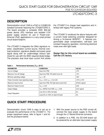
PHYTO37V to57VPSEFROMTXTX RXRX PWRGDTP1645.3 1%R17FOR NON-ISLATED DESIGNFOR NO-OPTO DESIGNS.ADD C13 ON TOP OF R11.[1][2][3]87654321100nFITHC2D2SMAJ58ANOTES: UNLESS OTHERWISE SPECIFIED,TP10TP9TP14PGNDTP15SIGNATURE 28E-L12VPORTN 220K1206C9Q1C30.1uF10V1uFR10 80.6k 1%R6 OPT 0805R9 OPT 1206VCC1MMBTA4232C1Q2VU1 [2]4.7KR73FDC2512VOUT VVOUTC40.1uF1.5K22nFR11[3] 156PA1277NL421456DISABLEI M INENABL EOPTCo4100uF6.3V3 UT3.3V/3A VOUTR15 100K47pFD9GRNR19150VOUTQUICK START GUIDE FOR DEMONSTRATION CIRCUIT 1249POE TO 3.3V@3.0A ISOLATED5
trip point, the Power Good signal goes active low and the amperage through the power switch is held below the high-level current limit. For the PD to remain powered on, it must present to the PSE both AC and DC components of the Maintain Power Signature (MPS). The PD must hold the DC MPS by drawing at least 10mA or the