Transcription
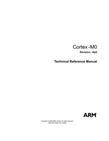
SoC FPGA ARM Cortex-A9 MPCoreProcessor Advance Information BriefAIB-01020-1.1Advance Information BriefThis document describes the dual-core ARM Cortex -A9 MPCore processorintegrated in the hard processor system (HPS) of the Altera Cyclone V and Arria Vsystem on a chip (SoC) FPGAs. This innovative HPS contains a microprocessor unit(MPU) with a dual-core ARM Cortex-A9 MPCore 32-bit application-class processor,memory controllers, and a rich set of system peripherals, hardened in Altera's mostadvanced 28-nm FPGA fabric. These SoC FPGAs provide the performance, power,and cost savings of hard logic, with the flexibility and time-to-market benefits ofprogrammable logic.ARM Cortex-A9 MPCore Processor ArchitectureARM processors are the standard in embedded systems. Altera SoC FPGAs leverageone of ARM's latest, high-performance Cortex-A9 processor architectures. TheCortex-A9 architecture provides industry-leading performance, the latest ARMfeatures and capabilities, and is widely deployed in products ranging from wirelesshandsets to tablet computers. Figure 1 shows the progression of ARM processorperformance and capability.Figure 1. ARM Processor Family LineupCortex-A15Cortex-R7Application Processors(Cortex-A Series)Performance and FunctionalityReal-Time Control(Cortex-R -M1ARM7Cortex-M0Capability101 Innovation DriveSan Jose, CA 95134www.altera.comFebruary 2012 2012 Altera Corporation. All rights reserved. ALTERA, ARRIA, CYCLONE, HARDCOPY, MAX, MEGACORE, NIOS,QUARTUS and STRATIX words and logos are trademarks of Altera Corporation and registered in the U.S. Patent and TrademarkOffice and in other countries. All other words and logos identified as trademarks or service marks are the property of theirrespective holders as described at www.altera.com/common/legal.html. Altera warrants performance of its semiconductorproducts to current specifications in accordance with Altera's standard warranty, but reserves the right to make changes to anyproducts and services at any time without notice. Altera assumes no responsibility or liability arising out of the application or useof any information, product, or service described herein except as expressly agreed to in writing by Altera. Altera customers areadvised to obtain the latest version of device specifications before relying on any published information and before placing ordersfor products or services.ISO9001:2008RegisteredAltera CorporationSubscribe
ARM Cortex-A9 MPCore Processor ArchitecturePage 2The dual-core ARM Cortex-A9 MPCore processor in Altera SoC FPGAs is designedfor maximum performance and power efficiency, implementing the widely-supportedARMv7 instruction set architecture to address a broad range of industrial,automotive, and wireless applications. The Cortex-A9 MPCore processor architectureincludes the following features:1 Dual-core multiprocessing, supporting both symmetric multiprocessing (SMP)and asymmetric multiprocessing (AMP) Multi-issue superscalar, out-of-order, speculative execution 8-stage pipelinedelivering 2.5 DMIPS/MHz per CPU Advanced branch prediction Single- and double-precision IEEE standard 754-1985 floating-point mathematicaloperations ARM NEON 128-bit single instruction multiple data (SIMD) media processingengine Jazelle byte-code dynamic compiler support TrustZone architecture for enhanced system securityFor more details about ARM Cortex-A9 processors, refer to the ARM Cortex-A9Processors white paper.As shown in Figure 2, the Cortex-A9 processor architecture supports the ARMperformance-optimized instruction set and the latest memory-optimized Thumb -2mixed instruction set.SoC FPGA ARM Cortex-A9 MPCore Processor Advance Information BriefFebruary 2012Altera Corporation
ARM Cortex-A9 MPCore Processor ArchitecturePage 3Figure 2. ARM Processor Family Architectural FeaturesApplication and orsProcessor Architecture(Increasing rtex-M3Cortex-M1Cortex-R4Cortex-M4Cortex-M0ARM Performance-Optimized 32-bit Instruction SetArchitectural FeaturesThumb 16-bitInstruction SetThumb-2 Memory-Optimized Instruction SetIEEE-754 Floating Point ArithmeticJazelle Bytecode Dynamic Compiler SupportNested VectoredInterruptsWake-up InterruptControllerTrustZone System SecuritySingle Instruction Multiple Data(SIMD) ProcessingNEON Media EngineVirtualizationThe Thumb-2 instruction set optimizes processing performance in systems withnarrow memory data paths and improves energy efficiency. On average, Thumb-2code has a 31% smaller memory footprint and runs 38% faster than the originalThumb instruction set.SoC FPGA ARM Cortex-A9 MPCore Processor Advance Information BriefFebruary 2012Altera Corporation
Cache MemoryPage 4Figure 3 provides a detailed block diagram of the MPU subsystem. The MPUsubsystem includes two Cortex-A9 processor cores, the level 2 (L2) cache and memorysubsystem, Snoop Control Unit (SCU), Accelerator Coherency Port (ACP), and debugfunctions.Figure 3. MPU SubsystemDebuggingCoreSight Multicore Debug & TraceCross TriggeringEvent TracePerformance MonitorPerformance MonitorProgram TraceProgram TraceProcessor Cores& L1 CacheInterrupt ControllerJazelle BytecodeDynamic CompilerIEEE 754 Floating Point(single-,double-Precision)NEON DSP/Media SIMDProcessing EngineJazelle BytecodeDynamic CompilerIEEE 754 Floating Point(single-,double-Precision)NEON DSP/Media SIMDProcessing Engine800 MHzARM Cortex-A932-bit Dual-IssueSuperscaler RISC CPU800 MHzARM Cortex-A932-bit Dual-IssueSuperscaler RISC CPU32-KBL1 DataCache32-KBInstructionCache32-KBL1 gTimerL2 CachePrivate MMU withTrustZone SecurityPrivate MMU withTrustZone SecurityACPSCUCacheLockdownSupport512-KB L2 UnifiedCache with ECCCache MemoryCache memory improves the performance of a processor-based system and helpsreduce power consumption. Cache memory that is tightly integrated with anassociated processor core is called level 1 (L1) cache. Each Cortex-A9 CPU has twoindependent 32-kilobyte (KB) L1 caches—one for instructions and one for data—allowing simultaneous instruction fetches and data access. Each L1 cache is 4-way setassociative and has an eight-word line length.SoC FPGA ARM Cortex-A9 MPCore Processor Advance Information BriefFebruary 2012Altera Corporation
Cache MemoryPage 5The HPS also includes a 512-KB L2 shared, unified cache memory (instruction anddata for both Cortex-A9 cores). The L2 cache is 8-way set-associative withprogrammable locking by line, way, and master. The L2 cache includes errorcorrection code (ECC) reporting.Snoop Control Unit (SCU)The snoop control unit (SCU) is an integral part of the cache memory systems andmanages data traffic for the two Cortex-A9 CPUs and the memory system, includingthe L2 cache. In a multiprocessor system, each CPU may operate on shared data. TheSCU ensures that each processor core operates on the most up-to-date copy of data,maintaining cache coherency. Figure 4 shows the coherent memory, SCU, and ACP.Figure 4. Coherent Memory, SCU, and ACPyBidirectional CoherencyARM CortexARM Cortex-A932-bit Dual-I32-bit Dual-IssueSuperscaler RISC CPU Superscaler RISCoherent MemoryFPGAFabricHPSPeripheralsL3InterconnectL1 DataCacheACP IDMapperACP32-BitInstructionCacheSCU3L1 Data InsCacheCSCUL2Unified CacheThe SCU maintains bidirectional coherency among the L1 data caches ensuring bothCPUs access to the most recent data. When a CPU writes to any coherent memorylocation, the SCU ensures that the relevant data is coherent(updated/tagged/invalidated). Similarly, the SCU monitors read operations from acoherent memory location. If the required data is already stored in the L1 caches, thedata is returned directly to the requesting CPU. If the data is not in the L1 cache, theL2 cache checks its contents before the data is finally retrieved from the main memory.The SCU also manages accesses from the ACP and arbitrates between the Cortex-A9CPUs if both attempt simultaneous access to the L2 cache.Accelerator Coherency PortThe ACP allows level 3 (L3) interconnect masters—such as Ethernet media accesscontroller (EMAC), direct memory access (DMA), and FPGA-to-HPS bridge—to sharedata coherently with the MPU subsystem. With the ACP, read accesses to coherentmemory regions always return the most current data, whether in L1 cache, L2 cache,or main memory. Similarly, write operations to coherent memory regions cause theSCU to force coherence before the data is forwarded to the memory system.SoC FPGA ARM Cortex-A9 MPCore Processor Advance Information BriefFebruary 2012Altera Corporation
IEEE standard 754-1985 Floating Point UnitPage 6The ACP ID mapper is located between the L3 interconnect and the ACP. The ARMACP port is designed to support up to eight unique transactions concurrently (eightunique transaction IDs are supported). However, the FPGA fabric can have anynumber of masters requesting coherent transactions. The ACP mapper dynamicallyallocates the available eight transaction IDs to the requesting masters to ensure that allmasters have access to coherent memory regions.IEEE standard 754-1985 Floating Point UnitBoth ARM Cortex-A9 processor cores include full support for IEEE standard 754-1985floating-point operations—important for imaging, signal processing, scientificcomputing, and graphics.The floating-point unit (FPU) fully supports single- and double-precision add,subtract, multiply, divide, multiply/accumulate, and square-root operations. The FPUalso converts between floating-point data formats and integers, including specialoperations to round-towards-zero required by high-level languages.The FPU greatly increases performance for applications that heavily rely onfloating-point arithmetic operations such as advanced control algorithms, imaging(scaling, 3D transforms), fast Fourier transforms (FFT), and digital filtering ingraphics.NEON Media Processing EngineBoth of the ARM Cortex-A9 processor cores include an ARM NEON mediaprocessing engine (MPE) that supports simultaneous operations on multiple data,also called SIMD processing, shown in Figure 5. The NEON processing engineaccelerates multimedia and signal processing algorithms, such as videoencoding/decoding, 2D/3D graphics, audio and speech processing, imageprocessing, telephony, and sound synthesis. The SIMD architecture completes somesignal processing algorithms up to eight times faster than a scaler processor.Figure 5. SIMD ProcessingSingle Instruction Multiple Data (SIMD)Source RegisterSource RegisterOpOpOpOpDestination RegisterSoC FPGA ARM Cortex-A9 MPCore Processor Advance Information BriefFebruary 2012Altera Corporation
Jazelle Dynamic Byte-Code Compiler SupportPage 7The Cortex-A9 NEON MPE performs operations on the following data types: SIMD and scalar single-precision floating-point computations Scalar double-precision floating-point computation SIMD and scalar half-precision floating-point conversion 8-, 16-, 32-, and 64-bit signed and unsigned integer SIMD computation 8- or 16-bit polynomial computation for single-bit coefficientsThe available operations include the following functionality:1 Addition and subtraction Multiplication with optional accumulation Maximum or minimum value-driven lane selection operations Inverse square-root approximation Comprehensive data-structure load instructions, includingregister-bank-resident table lookupFor more details on the ARM NEON processing engine, including applicationbenchmarks, refer to the NEON Technology Introduction presentation.Jazelle Dynamic Byte-Code Compiler SupportEach Cortex-A9 CPU includes support for ARM Jazelle technology, a combinedhardware and software solution. ARM Jazelle software is a full-featured,multi-tasking Java Virtual Machine (JVM), highly optimized to exploit Jazellearchitecture extensions.The ARM Jazelle Direct Bytecode eXecution (DBX) technology supports directexecution of Java bytecodes. This flexibility allows a Cortex-A9 processor to efficientlyrun an established operating system, middleware, and Java applications.The ARM Jazelle Runtime Compilation Target (RCT) technology supports efficientahead-of-time (AOT) and just-in-time (JIT) compilation with Java and other executionenvironments.TrustZone System-Wide SecurityARM's TrustZone technology lets you create secure subsystem extensions throughoutthe HPS and FPGA fabric. This system-wide approach enables secure transactionsbetween the processors, peripherals, and memory, ensuring that errant or malicioussoftware cannot interact with or record data traffic between devices in the securedomain.The processor, DMA controller, and FPGA-to-HPS bridge support security on a pertransaction basis. The SDRAM controller subsystem supports secure and non-secureregions for each port of the SDRAM multiport front end. At boot time the processorsand slave ports in the system are set to a secure state. The security settings for most ofthe slave ports can be modified under software control.SoC FPGA ARM Cortex-A9 MPCore Processor Advance Information BriefFebruary 2012Altera Corporation
Generic Interrupt ControllerPage 8Generic Interrupt ControllerThe Generic Interrupt Controller (GIC) is shared by both Cortex-A9 CPUs, as shownin Figure 6. There are over 130 unique interrupt sources, including the dedicated HPSperipherals and functions implemented in the FPGA fabric. There are up to 64 uniqueinterrupts originating from IP in the FPGA fabric. The FPGA configuration managerand the timeout signals from the FPGA-to-HPS and HPS-to-FPGA bus bridges arealso potential interrupt sources.Figure 6. Interrupts Sources to Interrupt ControllerInterrupt SourcesARM Cortex-A9CPU0/CachesARM Cortex-A9CPU1/CachesSCUSnoop Control UnitL2 CacheDDR SDRAMARM Cortex-A9CPU 0DMA ControllerEthernet 1:0USB 1:0CAN 1:0MMC/SDNAND FlashQuad SPI FlashGenericInterruptControllerSPI 3:0I2C 3:0UART 1:0GPIO 2:0Timer 3:0Watchdog 1:0PLL LockFPGA ManagerARM Cortex-A9CPU 1FPGA-based IPFPGA2SoCBridge TimeoutSoC2FPGABridge TimeoutFor some peripherals, such as the USB controllers, multiple interrupt sources arecombined to a single interrupt to the processors. Each USB controller supports up to32 interrupts from individual USB endpoints, all of which are combined into a singleinterrupt to the processor.Private CPU TimersAs shown in Figure 3, each Cortex-A9 processor contains both private timers andshares a global timer. Private timers are only accessible from the associated processorcore. Each CPU has a private 32-bit interval timer and a private 32-bit watchdog timer.The 32-bit interval timer has a programmable 8-bit prescaler, supports single-shot orauto-reload modes, and has an optional processor interrupt.SoC FPGA ARM Cortex-A9 MPCore Processor Advance Information BriefFebruary 2012Altera Corporation
HPS Boot OptionsPage 9The 32-bit watchdog timer is primarily designed to react to errant programs byresetting the CPU. When the watchdog timer is enabled, application software mustperiodically reset the counter. If the counter reaches zero, it implies that theapplication software is stuck in an infinite loop or is otherwise locked. When thewatchdog timer reaches zero, the system resets the CPU. If not used as a watchdogtimer, it becomes an optional second interval timer.Shared Global TimerBoth CPUs share a global 64-bit auto-incrementing timer, which is primarily used bythe operating system. Each CPU has a private 64-bit compare value that generatesprivate interrupts when the counter reaches the specified value.HPS Boot OptionsThe HPS of the Altera SoC FPGA can operate independently from the FPGA fabric.The processor booting does not depend upon the FPGA fabric, unless desired.After a power-on reset or processor reset, one processor begins executing from an onchip RAM containing the primary bootloader program while the second processor isheld in reset. The boot processor reads the state of three boot select pins that specifywhere the initial software image is stored, typically in flash memory. In the case of aboot from flash memory, the ROM code initializes the boot source interface, copies theinitial software image to the internal SRAM, and then executes the program. Theinitial software image includes the entry point to the user's application softwareimage. In the case of a boot from the FPGA fabric, the CPU waits until the FPGAfabric reports that it is configured and has entered user mode before the initialsoftware image is copied from the FPGA fabric to internal SRAM and programexecution begins.The processor can boot from any of the following sources: External Quad Shared Peripheral Interrupt (SPI) flash memory (NOR) External NAND flash memory (Open NAND Flash Interface (ONFI)1.0-compliant) External MultiMediaCard (MMC)/Secure Digital (SD) flash memory Via the FPGA fabric—the CPU waits until the FPGA fabric reports that it isconfigured and has entered user modeThe initial software image also contains various elements to protect the image againstaccidental or intentional modification. If the processor cannot successfully boot fromthe specified location, the HPS automatically reverts to the location of the last imageloaded. If there are no previous images loaded, then the system attempts to boot fromthe FPGA fabric.SoC FPGA ARM Cortex-A9 MPCore Processor Advance Information BriefFebruary 2012Altera Corporation
System InterconnectPage 10System InterconnectThe remainder of the HPS is located outside of the MPU subsystem, as shown inFigure 7. The processor accesses the rest of the HPS through a pair of 64-bit AdvancedMicrocontroller Bus Architecture (AMBA ) Advanced eXtensible Interface (AXI )masters. The high-bandwidth peripherals, including the FPGA data ports, connect tothe L3 interconnect structure. The L3 interconnect is further partitioned into threemajor sub-switches. The L3 interconnect uses a multilayer, non-blocking architecturethat supports multiple, simultaneous transactions between peripherals, sub-switches,SDRAM, and the MPU subsystem. Each L3 bus master has programmable priority.SoC FPGAs use the 32-bit AMBA High-performance Bus (AHB ) as a low-power busto low-power peripherals, and high-performance 64-bit AXI to high-performanceperipherals. The lower-bandwidth peripherals reside on the level 4 (L4) bus,implemented as a 32-bit ARM Advanced Peripheral Bus (APB ). Some peripherals,like the DMA controller, have low-bandwidth control connections on the L4interconnect and high-bandwidth data transfer connections on the L3 interconnect.SoC FPGA ARM Cortex-A9 MPCore Processor Advance Information BriefFebruary 2012Altera Corporation
System InterconnectPage 11Figure 7. SoC FPGA Hard Processor System ConnectionsFPGA-to-HPSFPGAControlBlockHPS-to-FPGA LW HPS-to-FPGA 64/128L4, ABridgeAXI-32LW HPS-toFPGA BridgeAXI-64AXI-32L3 Interconnect(NIC-301)DAPMulti-port AXI/Avalon-MMMasterAXISlaveMPU SubsystemAXI-64ARM Cortex-A9 MP 2ACP IDMapperAXI-64AHB-32L3 MasterPeripheralSwitchAXI-32ACPCPU1SCUL2 CacheL3 Main NDAXI-32AXI-64AXI-32AXI-32AHB-32L3 Slave Peripheral SwitchAHB-32AHB-32DMAQSPIL4, )SystemManagerSoC FPGA ARM Cortex-A9 MPCore Processor Advance Information uary 2012Altera Corporation
Page 12SoC FPGA System Address MapTable 1 lists the connections between the various system bus masters and slaves. Notevery bus master communicates with every bus slave, although the MPU subsystem,the FPGA-to-HPS bridge, lightweight HPS-to-FPGA bridge, and the Debug AccessPort (DAP) have universal access.LWHPS2FPGAREGSSDRAM PIDATANAND DATANAND REGSUSB1USB0FPGA2HPSREGSFPGA2HPSREGSL4SlavesTable 1. Master/Slave Connection MatrixMastersMPU subsystemv v v v v v v v v v — v v v vFPGA-to-HPSv v v v v v v v v v v v v v vDMAv — — — — — v v v v v — v v vEMAC0— — — — — — — — — v v — v v vEMAC1— — — — — — — — — v v — v v vUSB0— — — — — — — — — v v — v v vUSB1— — — — — — — — — v v — v v vNAND— — — — — — — — — v v — v v vSD/MMC— — — — — — — — — v v — v v vEmbedded TraceRouter (ETR)— — — — — — — — — v — — v v vDebug Access Portv v v v v v v v v v v — v v vSoC FPGA System Address MapThe HPS address map specifies the addresses of slaves such as memory andperipherals as viewed by the MPU and other masters.The HPS has multiple address spaces that are either contained inside the HPS or are atthe boundary between the FPGA fabric and HPS. Each address space in the HPSsystem address map is 4 GB in total, as shown in Table 2 and Figure 8.Table 2. HPS Address SpacesNameSizeMastersMPU4 GBMPUL34 GBAll L3 masters except MPUFPGASLAVESUnlimitedAll L3 masters accessing HPS-to-FPGA AXI bridgeLWFPGASLAVESUnlimitedAll L3 masters accessing lightweight HPS-to-FPGA AXI bridgeFebruary 2012Altera CorporationSoC FPGA ARM Cortex-A9 MPCore Processor Advance Information Brief
SoC FPGA System Address MapPage 13Figure 8 shows the relationships between the HPS address spaces. Some addressspaces have windows into other address spaces. The thin colored arrows indicatewindows mapped to other address ranges (the arrows point to mapped addressspaces). For example, the ACP window in the L3 address space provides access intothe bottom 1 GB of the CPU address space. The vertical arrows in the SDRAMwindow of the CPU address space shows that the boundaries of the SDRAM windowcan be moved in the direction of the arrows.Figure 8. HPS Address PeripheralFPGAWindowFPGAWindowSDRAM4 GB3 GBACPWindowSDRAM2 GBSDRAMWindowSDRAMWindow1 GBBoot0 GBThe top 64 megabytes (MB) in the CPU and L3 address spaces is always allocated tothe HPS dedicated peripherals. The CPU and L3 peripherals support up to 1 GB ofaddress space to communicate with slave peripherals in FPGA fabric, minus the64 MB at the top allocated to the HPS dedicated peripherals.You can address architecture on the FPGA fabric without limits. A 1 MB window inthe address map allows sharing between the FPGA fabric and the HPS. (soft logic inthe FPGA fabric performs address decoding). The L3 and CPU address spacesprovide a window of nearly 1 GB (1 GB minus 64 MB for peripherals) into the FPGAaddress space.After power-on or a cold or warm reset, the bottom 1 MB is allocated to the boot ROMfor the MPU subsystem and L3 masters. Under software control, the lower 1 MB canbe remapped to the 64 KB on-chip RAM, or the bottom 1 MB of external SDRAM.The MPU subsystem directly addresses a minimum of nearly 3 GB. The L3 masterssupport up to 2 GB of SDRAM. Access to coherent memory from the L3 masters isperformed via the 1 GB of address space allocated to the ACP, as described in“Accelerator Coherency Port” on page 5.SoC FPGA ARM Cortex-A9 MPCore Processor Advance Information BriefFebruary 2012Altera Corporation
Page 14Communication Between the HPS and FPGA FabricBesides transactions over the system bus, IP implemented in the FPGA fabric have aseparate private data path to the full 4 GB of SDRAM.Communication Between the HPS and FPGA FabricSystems implemented with separate CPU and FPGA devices usually suffer fromcommunication bottlenecks between the two devices. Although the HPS and theFPGA fabric can operate entirely independently in the SoC FPGA, they share twohigh-bandwidth, 128-bit AMBA AXI bus bridges called FPGA-to-HPS andHPS-to-FPGA bridges. IP built in the FPGA fabric have access to HPS L3 and L4slaves via the FPGA-to-HPS bridge. Similarly, HPS L3 masters have access to slaves inthe FPGA fabric via the HPS-to-FPGA bridge. Both bridges have configurable datapath widths of 32, 64, or 128 bits. The variable data width allows the data rate to betuned when crossing between the FPGA fabric and HPS L3 buses to maximize systemperformance. For example, 64-bit wide transactions from a 400-MHz L3 master switchcan be rate-matched to 128-bit wide transactions at 200MHz into the FPGA fabric.An additional lightweight HPS-to-FPGA bridge provides accesses to the control andstatus register (CSR) slave ports in the FPGA fabric. Use of this bridge frees up theremaining HPS-to-FPGA bridge to perform high speed bursting transactions. Thelightweight HPS-to-FPGA bridge is 32-bit because CSR slaves are typically 32 bitswide.All communication from the FPGA fabric side is synchronized by a locally-providedclock source. Similarly, the L3 interconnect has its own clock source. The SoC FPGAprovides the necessary asynchronous clock-crossing logic between the two domains.The FPGA-to-HPS and HPS-to-FPGA bus bridges are AMBA AXI-3 compatible. Inaddition, the FPGA fabric supports other bus interface standards. Altera's Qsyssystem integration tool allows you to connect soft logic in the FPGA based on AMBAAXI-3, Avalon Memory-Mapped (Avalon-MM), and Avalon Streaming (Avalon-ST)interface standards. Qsys creates a high-performance network-on-a-chip (NoC)interconnect in the FPGA fabric that allows components, based on different busstandards, to communicate seamlessly.You can flag transactions over the FPGA-to-HPS bridge as TrustZone secure ornon-secure on a per-transaction basis. Transactions over the HPS-to-FPGA bridges aresecure during the boot process, but they can be secured or unsecured throughsoftware control.System-Level ManagementThe HPS and the FPGA fabric are both stand-alone entities that can operateindependently from one another. However, the HPS can directly configure andmonitor the FPGA fabric via the FPGA configuration manager.Beyond the SoC FPGA's on-chip FPGA fabric, the processor can also configureadditional external FPGAs from the same configuration memory source.February 2012Altera CorporationSoC FPGA ARM Cortex-A9 MPCore Processor Advance Information Brief
System-Level ManagementPage 15FPGA ManagerThe FPGA manager is a 32-bit peripheral, as shown in Figure 9. The configurationinterface is familiar to existing Altera FPGA designers and is similar to the passiveparallel configuration mode used to configure other Altera FPGA devices from anexternal processor. In addition to the ability to program the FPGA fabric from theHPS, the FPGA fabric also supports configuration from external, active, or passivesources.The FPGA manager provides various configuration options: Configure the full FPGA Configure just the I/O and have the remainder of the FPGA configured overthe PCI Express (PCIe ) port Partially reconfigure portions of the FPGA fabric Provide decompression on a compressed bitstream image Decrypt an FPGA bitstream previously encrypted using Advanced EncryptionStandards AES, thereby providing an additional layer of system security In high-reliability applications, perform bitstream scrubbing to further protectagainst single event upsets (SEUs)Figure 9. FPGA ManagerSoC FPGAFPGAnCONFIGMSEL,nCE,DCLK,DATA,PR REQUESTOnlynSTATUS &CONF DONExxVCCPGMConfigurationBlock10 kΩxxnSTATUS,CONF DONE,INIT DONEOnlynSTATUS &CONF DONECONFIG IOModeHPSFPGAManagerBesides configuring the internal FPGA fabric, the HPS can optionally program otherFPGAs in the system. The CPU controls the CONF DONE pin and can delaycompletion of multi-FPGA configurations.Clock ManagerThe clock manager generates and manages all the system clocks in the HPS.SoC FPGA ARM Cortex-A9 MPCore Processor Advance Information BriefFebruary 2012Altera Corporation
Page 16System-Level ManagementThe clock manager controls the three primary phase-locked loops (PLLs), includingthe output frequency generated, the phase, and the delay from the selected clockinput. Similarly, the CPU can monitor the lock status for each PLL.Table 3 shows the clock sources for each of the PLLs.Table 3. Clock Sources for Clock Manager PLLsPrimary OscillatorInputSecondary OscillatorInputFrom FPGA FabricReference ClockMain PLLv——SDRAM PLLvvSDRAM reference clockPeripheral PLLvvPeripheral reference clockPLLThe HPS architecture automatically handles signals that cross between clock domains.Reducing the clock frequency helps reduce overall system power consumption.Under processor control, the clock manager can change the main system clockwithout affecting the clocks controlling the peripherals or SDRAM interface. Directlychanging the PLL's operating frequency using the multiply and divide valuesprovides fine-grain frequency control and long settling times between changes.Changing the post-scale counters associated with the PLL results in quick changes,but with reduced frequency resolution.Reset ManagerThe reset manager determines the source and type of reset to the system and performsany necessary prequalification of a reset signal before forwarding it to the HPS orFPGA fabric. Based on the type of reset, a reset signal might reset only a portion of theentire device.In the HPS, there are three reset request types: Cold reset—forces the entire HPS, including debugging functions, into aknown default state to begin/restart the boot process. Warm reset—recovers a non-responsive system. This reset only affects aportion of the system and not the debugging infrastructure described in“Debugging Infrastructure” on page 17. A warm reset does not clear thesystem configuration options set during a cold reset or power-on condition. Debug reset—recovers only debug and trace functions should they becomenonresponsive.Global cold reset requests reset the entire device. The following sources can initiate acold reset request:February 2012 The power-on reset (POR) monitor The nPOR input pin Cold reset request from FPGA fabric Software-based cold
multi-tasking Java Virtual Machine (JVM), highly optimized to exploit Jazelle architecture extensions. The ARM Jazelle Direct Bytecode eXecut ion (DBX) technology supports direct execution of Java bytecodes. This flexibilit y allows a Cortex-A9 processor to efficiently run an established operating system, middleware, and Java applications.