Transcription
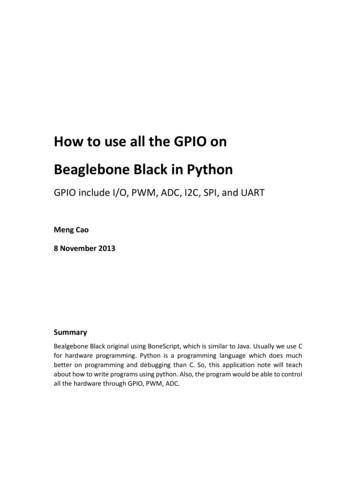
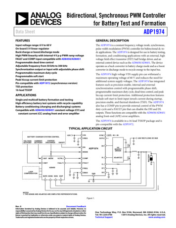
Bidirectional, Synchronous PWM Controllerfor Battery Test and FormationADP1974Data SheetFEATURESGENERAL DESCRIPTIONInput voltage range: 6 V to 60 VOn-board 5 V linear regulatorBuck/charge or boost/discharge modeHigh PWM linearity with internal 4 V p-p PWM ramp voltageFAULT and COMP input compatible with AD8450/AD8451Programmable dead time controlAdjustable frequency from 50 kHz to 300 kHzSynchronization output or input with adjustable phase shiftProgrammable maximum duty cycleProgrammable soft startPeak hiccup current-limit protectionPin-compatible with ADP1972 (asynchronous version)TSD protection16-lead TSSOPThe ADP1974 is a constant frequency, voltage mode, synchronous,pulse-width modulation (PWM) controller for bidirectional dc-todc applications. The ADP1974 is designed for use in battery testing,formation, and conditioning applications with an external, highvoltage field effect transistor (FET) half bridge driver, and anexternal control device such as the AD8450/AD8451. The deviceoperates as a buck converter in battery charge mode and as a boostconverter in discharge mode to recycle energy to the input bus.The ADP1974 high voltage VIN supply pin can withstand amaximum operating voltage of 60 V and reduces the need foradditional system supply voltages. The ADP1974 has integratedfeatures such as precision enable, internal and externalsynchronization control with programmable phase shift,programmable maximum duty cycle, dead time control, and peakhiccup current-limit protection. Additional protection featuresinclude soft start to limit input inrush current during startup,precision enable, and thermal shutdown (TSD). The ADP1974also has a COMP pin to provide external control of the PWMduty cycle and a FAULT pin that can disable the DH and DLoutputs. These functions are compatible with the AD8450/AD8451analog front-end (AFE) error amplifiers.APPLICATIONSSingle and multicell battery formation and testingHigh efficiency battery test systems with recycle capabilityBattery conditioning (charging and discharging) systemsCompatible with AD8450/AD8451 constant voltage (CV) andconstant current (CC) analog front end error amplifierThe ADP1974 is available in a 16-lead TSSOP package and ispin-compatible with the ADP1972.TYPICAL APPLICATION CIRCUITBATTERY CHARGER SYSTEM CFG 24V RECYLCING DC BUSON/OFFDHENADP1974MODEISET ETPOINT 24VGNDSS12699-001BVP0 BVN0 ISVN ISVP –– NOTES1. THE AD8450 AND ADuM7223 ARE SIMPLIFIED REPRESENTATIONS.Figure 1.Rev. 0Document FeedbackInformation furnished by Analog Devices is believed to be accurate and reliable. However, noresponsibility is assumed by Analog Devices for its use, nor for any infringements of patents or otherrights of third parties that may result from its use. Specifications subject to change without notice. Nolicense is granted by implication or otherwise under any patent or patent rights of Analog Devices.Trademarks and registered trademarks are the property of their respective owners.One Technology Way, P.O. Box 9106, Norwood, MA 02062-9106, U.S.A.Tel: 781.329.4700 2015 Analog Devices, Inc. All rights reserved.Technical Supportwww.analog.com
ADP1974Data SheetTABLE OF CONTENTSFeatures . 1External COMP Control . 12Applications . 1Peak Current-Limit Hiccup Implementation . 12General Description . 1Negative Current-Limit Detection (Buck Mode) . 13Typical Application Circuit . 1PWM Frequency Control. 13Revision History . 2Maximum Duty Cycle . 13Specifications. 3External Fault Signaling . 13Absolute Maximum Ratings. 5Thermal Shutdown (TSD) . 13Thermal Operating Ranges . 5Applications Information . 14ESD Caution . 5Buck or Boost Selection. 14Pin Configuration and Function Descriptions . 6Selecting RS to Set the Current Limit . 14Typical Performance Characteristics . 7Adjusting the Operating Frequency . 14Theory of Operation . 10Programming the Maximum Duty Cycle . 16Supply Pins . 10Adjusting the Soft Start Period . 16EN/Shutdown. 11PCB Layout Guidelines . 18Undervoltage Lockout (UVLO) . 11Outline Dimensions . 19Soft Start . 11Ordering Guide . 19Operating Modes . 11PWM Drive Signals . 12REVISION HISTORY9/15—Revision 0: Initial VersionRev. 0 Page 2 of 19
Data SheetADP1974SPECIFICATIONSVIN 24 V and specifications valid for TJ 40 C to 125 C, unless otherwise specified. Typical values are at TA 25 C. All limits attemperature extremes are guaranteed via correlation using standard statistical quality control (SQC).Table 1.ParameterINPUT VOLTAGE (VIN)Voltage RangeVIN Supply CurrentVIN Shutdown CurrentUVLO Threshold RisingUVLO Threshold FallingSOFT START (SS)SS Pin CurrentSS Threshold RisingSS Threshold FallingEnd of Soft StartPWM CONTROLFREQFrequency RangeOscillator FrequencyFREQ Pin VoltageSYNC Output (Internal Frequency Control)Internal SYNC RangeSYNC Output Clock Duty CycleSYNC Sink ResistanceSYNC Input (External Frequency Control)External SYNC RangeSYNC Pull-Down ResistorMaximum SYNC Pin VoltageSYNC Threshold RisingSYNC Threshold FallingMinimum Pulse WidthSCFGSCFG High Threshold RisingSCFG High Threshold FallingSCFG Low Threshold RisingSCFG Low Threshold FallingSCFG Pin CurrentDMAXMaximum Internal Duty CycleDMAX Setting CurrentDMAX and SCFG Current Matching1COMPCOMP Pin Input Voltage RangeInternal Peak-to-Peak Ramp VoltageMaximum Internal Ramp VoltageMinimum Internal Ramp VoltageDTDT Pin CurrentMaximum DT Programming fSYNCTest .5kHzMΩVVVns4.712.5VVVVμA12.510%μA%6RFREQ 100 kΩ, VSS 0 V, SYNC floating,FAULT low, EN highVEN 0 VVIN risingVIN fallingVSS 0 VSwitching enable thresholdSwitching disable thresholdAsynchronous to synchronous thresholdRFREQ 33.2 kΩ to 200 kΩRFREQ 100 kΩRFREQ 100 kΩVSCFG 4.53 V or SCFG pin floatingFor SYNC outputVSCFG VVREG, RFREQ 100 kΩVSCFG 5 V, ISYNC 10 mAVSCFG 4.25 VFor SYNC input NC set to inputSYNC set to outputProgrammable phase shift above thresholdNo phase shiftRFREQ 100 kΩ, VSCFG GND0.49.54.534.510.520.511IDMAXVCOMP, VDMAX, VSS, and VSCFG 5 VVDMAX 0 V, RFREQ 100 kΩ9.59711VCOMPV p-p4.2500.45IDTVDTRFREQ 100 kΩ, VDT GNDRev. 0 Page 3 of 190.655.044.50.5200.55VV p-pVV223.5μAV
ADP1974ParameterPRECISION ENABLE LOGIC (EN)Maximum EN Pin VoltageEN Threshold RisingEN Threshold FallingEN Pin CurrentMODE LOGICMaximum MODE Pin VoltageMODE Threshold RisingMODE Threshold FallingCURRENT LIMIT (CL)Set CurrentBuck CL ThresholdBuck Negative Current ThresholdBoost CL ThresholdHiccup Detect TimeHiccup Off TimeVREGLDO Regulator Output VoltageGuaranteed Output CurrentLoad RegulationFAULTMaximum FAULT Pin VoltageFAULT Threshold RisingFAULT Threshold FallingFAULT Pin CurrentPWM DRIVE LOGIC SIGNALS (DH/DL)DL Drive VoltageDH Drive VoltageDL and DH Sink ResistanceDL and DH Source ResistanceDL and DH Pull-Down ResistorTHERMAL SHUTDOWN (TSD)TSD Threshold RisingTSD Threshold Falling1Data SheetSymbolTest Conditions/CommentsMinTyp1.11.251.220.32VEN 5 V, internal pull down0.7ICLVCL (BUCK)VNC (BUCK)VCL (BOOST)VVREGIOUT (MAX)VCL 0 VRFREQ 100 kΩ, 500 consecutive clock pulsesRFREQ 100 kΩ, 500 consecutive clock pulsesEN highVIN 6 V to 60 V, no external loadVIN 6 V, external loadVIN 6 V, IOUT 0 mA to 5 VFAULTVFAULT 5 V, internal 8.5 MΩ pull-down resistorVDLVDHMaxNo loadNo loadIDL 10 mAIDL 10 mA0.5VREGVREG1.21.41150135 C CThe DMAX and SCFG current matching specification is calculated by taking the absolute value of the difference between the measured ISCFG and IDMAX currents, dividingthem by the 11 μA typical value, and multiplying this answer by 100. I I DMAX DMAX and SCFG Current Matching (%) SCFG 10011 μA Rev. 0 Page 4 of 19
Data SheetADP1974ABSOLUTE MAXIMUM RATINGSTable 2.ParameterVIN, EN, FAULT to GNDSYNC, COMP, MODE, VREG to GNDDH, DL, SS, DMAX, SCFG, CL, DT,FREQ to GNDOperating Ambient Temperature RangeJunction TemperatureStorage Temperature RangeRating 0.3 V to 61 V 0.3 V to 5.5 V 0.3 V to VREG 0.3 V 40 C to 85 C125 C 65 C to 150 CStresses at or above those listed under Absolute MaximumRatings may cause permanent damage to the product. This is astress rating only; functional operation of the product at theseor any other conditions above those indicated in the operationalsection of this specification is not implied. Operation beyondthe maximum operating conditions for extended periods mayaffect product reliability.Absolute maximum ratings apply individually only, not incombination.In applications with high power dissipation and poor printedcircuit board (PCB) thermal resistance, the maximum ambienttemperature may need to be derated. In applications withmoderate power dissipation and low PCB thermal resistance,the maximum ambient temperature can exceed the maximumlimit when the junction temperature is within specificationlimits.The junction temperature (TJ) of the device is dependent on theambient temperature (TA), the power dissipation of the device(PD), and the junction to ambient thermal resistance of thepackage (θJA). Use the following equation to calculate themaximum junction temperature (TJ) from the ambienttemperature (TA) and power dissipation (PD):TJ TA (PD θJA)For additional information on thermal resistance, refer toApplication Note AN-000, Thermal Characteristics of ICAssembly.ESD CAUTIONTHERMAL OPERATING RANGESThe ADP1974 can be damaged when the junction temperaturelimits are exceeded. The maximum operating junctiontemperature (TJ MAX) takes precedence over the maximumoperating ambient temperature (TA MAX). Monitoring ambienttemperature does not guarantee that the junction temperature(TJ) is within the specified temperature limits.Rev. 0 Page 5 of 19(1)
ADP1974Data SheetPIN CONFIGURATION AND FUNCTION DESCRIPTIONSDL 116 CLDH 215 GND14 DTVIN 4EN 5ADP1974TOP VIEW(Not to Scale)13 SCFG12 FREQMODE 611 DMAXSYNC 710 SSFAULT 89COMP12699-002VREG 3Figure 2. Pin ConfigurationTable 3. Pin Function DescriptionsPin c Drive Output for the External Low-Side MOSFET Driver.Logic Drive Output for the External High-Side MOSFET Driver.Internal Voltage Regulator Output and Internal Bias Supply. A bypass capacitance of 1 μF or greater from this pinto ground is required.High Input Voltage Supply Pin (6 V to 60 V). Bypass this pin with a 4.7 μF capacitor to ground.Logic Enable Input. Drive EN logic low to shut down the device. Drive EN logic high to turn on the device.Mode Select. Drive MODE logic low to place the device in boost (recycle) mode. Drive MODE logic high to placethe device in buck (charge) mode of operation. The MODE status is sampled at EN rising or FAULT falling (see theOperating Modes section).Synchronization Pin. This pin is configured as an input (slave mode) with SCFG 4.51 V to synchronize the ADP1974to an external clock. This pin is an open-collector driver output with SCFG 4.53 V (or SCFG connected to VREG).When configured as an output, SYNC is used to synchronize with other channels; a 10 kΩ resistor to VREG can beused as a pull-up.Fault Input Pin. Drive FAULT low to disable the DL and DH drivers in the event of a fault. Drive FAULT high to enablethe DL and DH drivers. FAULT can also reset the mode of operation as described in the Operating Modes section.This pin was designed to interface with the overcurrent protection (OCP) or overvoltage protection (OVP) faultcondition on the AD8450/AD8451.PWM Modulator Input. This pin interfaces with an error amplifier output signal from the AD8450/AD8451. Thesignal on this pin is compared internally to the linear ramp to produce the PWM signal. Do not leave this pinfloating; see the External COMP Control section for additional details.Soft Start Control Pin. A capacitor connected from SS to ground sets the soft start ramp time. Soft start controls theDL and DL duty cycle during power-up to reduce the inrush current. Drive SS below 0.5 V to disable switching of DLand DH. During soft start, the ADP1974 operates in pseudosynchronous mode (see the Soft Start section).Maximum Duty Cycle Input. Connect an external resistor to ground to set the maximum duty cycle. If the 97%internal maximum duty cycle is sufficient for the application, tie this pin to VREG. If DMAX is left floating, this pinis internally pulled up to VREG.Frequency Set Pin. Connect an external resistor between this pin and ground to set the frequency between 50 kHzand 300 kHz. When the ADP1974 is synchronized to an external clock (slave mode), set the slave frequency to 90%of the master frequency by multiplying the master RFREQ value times 1.11.Synchronization Configuration Input. Drive VSCFG 4.53 V (typical) to configure SYNC as an output clock signal.Drive VSCFG 4.51 V (typical) to configure SYNC as an input. Connect a resistor to ground with 0.52 V VSCFG 4.53 V(typical) to introduce a phase shift to the synchronized clock. Drive VSCFG 0.5 V (typical) to configure SYNC as aninput with no phase shift. If SCFG is left floating, the SYNC pin is internally tied to VREG, and SYNC is configured asan output.Dead Time Programming Pin. Connect an external resistor between this pin and ground to set the dead time.Do not leave this pin floating.Power and Analog Ground Pin.Current-Limit Programming Pin. Connect a current sense resistor in series with the low-side FET source to measurethe peak current in the inductor. The current-limit thresholds can operate with a 20 kΩ resistor as described in thePeak Current-Limit Hiccup Implementation section.Rev. 0 Page 6 of 19
Data SheetADP1974TYPICAL PERFORMANCE CHARACTERISTICSVIN VEN VFAULT 24 V, VMODE VCL VSS VCOMP 0 V, TA 25 C, unless otherwise TEMPERATURE ( C)152433425160EN PIN VOLTAGE (V)Figure 6. EN Pin Current vs. EN Pin Voltage, VEN 5 V and VFAULT 0 V1.25TA 125 CTA 25 CTA –40 CRISING1.24EN PIN THRESHOLD (V)2015101.231.22FALLING6152433425160INPUT VOLTAGE (V)1.20–4012699-004065100Figure 7. EN Pin Threshold vs. Temperature, VFAULT 0 V5.00TA 125 CTA 85 CTA 25 CTA –40 C4.98SS PIN CURRENT (µA)1.830TEMPERATURE ( C)Figure 4. Shutdown Current vs. Input Voltage, VEN 0 V and VFAULT 0 V1.9–512699-0071.2151.71.61.51.4VIN 6VVIN 24VVIN 60V4.964.944.921.3615243342INPUT VOLTAGE (V)516012699-0054.90Figure 5. Nonswitching Quiescent Current vs. Input Voltage (SYNC Floating)Rev. 0 Page 7 of 194.88–4004080TEMPERATURE ( C)Figure 8. SS Pin Current vs. Temperature12012699-008SHUTDOWN CURRENT (µA)TA 125 CTA 25 CTA –40 C6Figure 3. Input Voltage (VIN) UVLO Threshold vs. Temperature,VFAULT 0 VNONSWITCHING QUIESCENT CURRENT 699-006EN PIN CURRENT (µA)VIN UVLO THRESHOLD (V)5.7
ADP1974Data Sheet21019097.7RFREQ (MASTER) (kΩ)17097.697.597.41501301109070TA 125 CTA 25 CTA –40 C5097.26152433425160INPUT VOLTAGE (V)30505.020250300TA 125 CTA 85 CTA 25 CTA –40 C5.0153503005.010VREG (V)RDMAX (kΩ)200Figure 12. RFREQ (MASTER) vs. Switching Frequency (fSET)TA 125 CTA 25 CTA –40 C400150fSET (kHz)Figure 9. Maximum Internal Duty Cycle vs. Input Voltage,RFREQ 100 kΩ, VCOMP 5 V, and No Load on DL, DH, or DMAX45010012699-01297.312699-009MAXIMUM INTERNAL DUTY CYCLE (%)97.82502001505.0055.0001004.995020406080100DUTY CYCLE (%)4.99012699-01006802433425160INPUT VOLTAGE (V)Figure 10. RDMAX vs. Duty Cycle, RFREQ 100 kΩ, VCOMP 5 V, andNo Load on DL or DH1001512699-01350Figure 13. VREG vs. Input Voltage, No Load5.020TA 125 CTA 25 CTA –40 C5.0155.005VREG .04.5VCOMP (V)5.04.9800123LOAD CURRENT (mA)Figure 14. VREG vs. Load CurrentFigure 11. Duty Cycle vs. VCOMP, RFREQ 100 kΩ, andNo Load on DL, DH, or DMAXRev. 0 Page 8 of 194512699-014TA 125 CTA 85 CTA 25 CTA –40 C2012699-011DUTY CYCLE (%)5.010
Data SheetADP1974175TEN1501VREG125RDT (kΩ)VIN 24VVCOMP 2.5VNO CSS210075SYNC350DL25100µs5.0GS/sCH1T 14.42% 10M POINTS7.00V0010020030040050060012699-016CH1 10.0V CH2 5.0VCH3 5.0V CH4 5.0V12699-0154700tDEAD (ns)Figure 18. DT Pin Resistance (RDT) vs. Dead Time (tDEAD)Figure 15. Startup4501400EN3503SSRSCFG (kΩ)2300VIN 24VVCOMP 2.5VCSS 0.1µFDH250200150100CH2 2.0VCH4 5.0VB :20.0MW50.0ns/pt A CH125.0ms/div 20.0MS/s2.6V034ENVIN 24VVCOMP 2.5VCSS 0.1µFSSDHDLCH1 5.0VCH3 5.0VCH2 2.0VCH4 5.0VB :20.0MW3.04.56.0Figure 19. RSCFG vs. Phase Time Delay (tDELAY)50.0ns/pt A CH125.0ms/div 20.0MS/s2.6V12699-04321.5tDELAY (µs)Figure 16. Buck Soft Start10Figure 17. Boost Soft StartRev. 0 Page 9 of 197.512699-030CH1 5.0VCH3 5.0V5012699-0414DL
ADP1974Data SheetTHEORY OF LECT15V5VVREGENM1DHVREG 8.5MΩ500mVICL20µASYNCDETECT1MΩVOUTM2BAND GAPVBG µASSCSSADP19741kΩ12699-018SS DISCHARGEFigure 20. Internal Block DiagramThe ADP1974 is a constant frequency, voltage mode, synchronous,PWM controller for bidirectional dc-to-dc applications. TheADP1974 is designed to be used with an external, high voltageFET half bridge driver, such as the ADuM7223, and an externalerror amplifier AFE device, such as the AD8450/AD8451, toimplement a battery testing, charging, and discharging system.The ADP1974 has a high input voltage range, multiple externallyprogrammed control pins, and integrated safety features. Inbuck mode, the device charges a battery and delivers energyfrom the input power source to the output. In boost mode, thedevice discharges a battery and delivers energy from the batteryto the input. In both modes, the ADP1974 operates as asynchronous controller for maximum efficiency.SUPPLY PINSThe ADP1974 has two voltage supply pins, VIN and VREG.The VIN pin operates from an external supply that ranges from6 V to 60 V and is the supply voltage for the internal linearregulator of the ADP1974. Bypass the VIN pin to ground with a4.7 μF or greater ceramic capacitor.The VREG pin is the output of the internal linear regulator. Theinternal regulator generates the 5 V (typical) rail that is usedinternally to bias the control circuitry and can be used externallyas a pull-up voltage for the MODE, SYNC, DMAX, and FAULTpins. Bypass the VREG pin to ground with a 1 μF ceramiccapacitor. VREG is disabled when EN is low and is active aslong as VIN is above the internal UVLO (5.71 V typical) andEN is high.Rev. 0 Page 10 of 19
Data SheetADP1974When operating with an input voltage above 50 V, additionalinput filtering is recommended. Figure 21 shows therecommended filter configuration.When the device shuts down or a fault is detected, an activeinternal 1 kΩ pull-down resistor on the SS pin discharges YNCHRONOUSOPERATIONFigure 21. Recommended Filter Configuration forInput Voltages Greater than 50 V0.52V0VEN/SHUTDOWNThe EN input turns the ADP1974 on or off and can operatefrom voltages up to 60 V. The EN pin is designed with precisionenable control. When the EN voltage is less than 1.22 V (typical),the ADP1974 shuts down, VREG is disabled, and both DL andDH are driven low. When the ADP1974 shuts down, the VINsupply current is 15 μA (typical). When the EN voltage is greaterthan 1.25 V (typical), the ADP1974 is enabled, and VREG rampsto 5 V.ENABLEADP1974BEGINREGULATION12699-020RSUPPLY 50VFigure 22. Soft Start DiagramIn addition to the EN pin, the device can be disabled via a faultcondition indicated by an internal TSD event, a UVLO conditionon VIN, or an external fault condition signaled via the FAULT pin.It is necessary to disable the device to change the operatingmode from buck to boost.The MODE pin controls the ADP1974 duty cycle generator andaffects the DL and DH signals during soft start. In buck mode,a DH pulse initiates the on time (or Phase 1). In boost mode, aDL pulse initiates the on time. For more information aboutbuck vs. boost operation, see the Operating Modes section.During soft start, the ADP1974 operates in asynchronous mode,and the synchronous FET is not driven. During the off cycle, thediode in parallel to the low-side FET (buck mode) or the highside FET (boost mode) conducts the current until it reaches zeroor the next cycle begins. After the soft start period is completed(SS 4.5 V), the ADP1974 switches to full synchronous mode.UNDERVOLTAGE LOCKOUT (UVLO)OPERATING MODESThe UVLO function prevents the IC from turning on when theinput voltage is below the specified operating range to avoid anundesired operating mode. When VIN rises, the UVLO doesnot allow the ADP1974 to turn on unless VIN is greater than5.71 V (typical). The UVLO disables the device when VINdrops below 5.34 V (typical). The UVLO levels have 370 mVof hysteresis to prevent the system from turning on and offrepeatedly when there is a slow voltage ramp on the VIN pin.The ADP1974 operates as a synchronous buck or boost controller.When the MODE pin is driven high, above the 1.20 V (typical)threshold, the ADP1974 operates in a buck configuration forbattery charging. If the MODE pin is driven low, below the1.05 V (typical) threshold, the ADP1974 operates in a boostconfiguration. A boost configuration is ideal for dischargingin battery formation applications. See Figure 23 and Figure 24for the ADP1974 behavior in each mode. When the ADP1974is enabled, the internal regulator connected to the VREG pin alsopowers up. On the rising edge of VREG, the state of the MODE pinis latched, preventing the mode of operation from being changedwhile the device is enabled. To change between boost and buckmodes of operation, shut down or disable the ADP1974, adjust theMODE pin to change the operating mode, and restart the system.SOFT STARTThe ADP1974 has a programmable soft start that preventsoutput voltage overshoot during startup. When the ADP1974 isenabled with the EN pin, the VREG voltage begins rising to 5 V.When VREG reaches 90% of its 5 V (typical) value, the 5 μA(typical) internal soft start current (ISS) begins charging the softstart capacitor (CSS), causing the voltage on the SS pin (VSS) to rise.While VSS is less than 0.52 V (typical), the ADP1974 switchingcontrol remains disabled. When VSS reaches 0.52 V (typical),switching is enabled. As CSS continues to charge and VSS rises, thePWM duty cycle gradually increases, allowing the outputvoltage to rise linearly. CSS continues to charge, and VSS rises tothe internal VREG voltage (5 V typical). When the system dutycycle set by COMP is less than the soft start duty cycle, the externalcontrol loop takes control of the ADP1974. See Figure 22 for asoft start diagram.The operating mode can be changed when the EN pin is drivenlow, the FAULT pin is driven low, or the ADP1974 is disabledvia a TSD event or UVLO condition. On the rising edge of theFAULT control signal, the state of the MODE pin is latched,preventing the mode of operation from being changed whilethe device is enabled.Rev. 0 Page 11 of 19
ADP1974Data SheetBOOST MODE CONFIGURATIONMODE 1.05V (TYPICAL)VSCFG 4.53V (TYPICAL)error signal increases or decreases. The internal PWM comparatordetermines the appropriate duty cycle drive signal by monitoringthe error signal at the COMP pin and the internal 4 V p-p rampsignal. The internal PWM comparator subsequently drives theexternal gate driver at the determined duty cycle through the DHand DL signals.4.5VCOMPINTERNAL RAMP(4V p-p)2.5V0.5V0VVREG (5V TYPICAL)DH0VVREG (5V TYPICAL)12699-021DL0VFigure 23. Drive Signal Diagram for Boost ConfigurationBUCK MODE CONFIGURATIONMODE 1.20V (TYPICAL)VSCFG 4.53V (TYPICAL)4.5V2.5VCOMPINTERNAL RAMP(4V p-p)The functional voltage range of the COMP pin is from 0 V to5.0 V. If VCOMP is between 0.5 V and 4.5 V, the ADP1974 regulatesthe DH and DL outputs accordingly. If VCOMP is greater than4.5 V, the ADP1974 operates the DH and DL outputs at themaximum programmed duty cycle (or 97% whichever is thelowest). If VCOMP is less than 0.45 V, the ADP1974 operates theDH or DL output at a 0% duty cycle, according to the operatingmode, while the complementary DL or DH output is driven at a100% duty cycle. The input to the COMP pin must neverexceed the 5.5 V absolute maximum rating.The DL and DH signals swing from VREG (5 V typical) toground. The external FET driver used must have input controlpins compatible with a 5 V logic signal.0.5V0VVREG (5V TYPICAL)PEAK CURRENT-LIMIT HICCUP IMPLEMENTATION0VDL0V12699-022VREG (5V TYPICAL)Figure 24. Drive Signal Diagram for Buck ConfigurationPWM DRIVE SIGNALSThe ADP1974 has two 5 V logic level output drive signals, DHand DL that are compatible with drivers similar to the ADuM7223.The DH and DL drive signals synchronously turn on and off thehigh-side and low-side switches driven from the external driver.The ADP1974 provides resistor programmable dead time toprevent the DH and DL pins from transitioning at the sametime, as shown in Figure 25. Connect a resistor to ground onthe DT pin to program the dead time.The ADP1974 features a peak hiccup current-limit implementationmeasured on the low-side FET across a sense resistor. When thepeak inductor current exceeds the programmed current limitfor more than 500 consecutive clock cycles, 5.2 ms (typical) fora 100 kHz programmed frequency, the peak hiccup currentlimit condition occurs. If the overcurrent exist for less than500 consecutive cycles, the counter is reset to zero. When theovercurrent condition occurs, the SS pin is discharged througha 1 kΩ resistor, and the drive signals, DL and DH, are disabledfor the next 500 clock cycles to allow the FETs to cool down (hiccupmode). When the 500 clock cycles expire, the ADP1974 restartsthrough a new soft start cycle.Figure 26 shows the current-limit block diagram for peak currentlimit protection.H BUCKL 2699-023DLHFigure 25. Dead Time (tDEAD) Between DH and DL TransitionsWhen driving capacitive loads with the DH and DL pins, a 20 Ωresistor must be placed in series with the capacitive load to reduceground noise and ensure signal integrity.EXTERNAL COMP CONTROLThe ADP1974 COMP pin is the input to the PWM modulatorcomparator. The ADP1974 uses a voltage mode control thatcompares an error signal, applied to the COMP pin by anexternal error amplifier, such as the AD8450/AD8451, to aninternal 4 V p-p triangle waveform. As the load changes, theCL300mVRCL20kΩRS12699-024DHFigure 26. Current-Limit Block Diagram for Peak Current-Limit ProtectionThe current-limit threshold is set internally based on the modeselected. It is designed to trigger when the voltage on RS reaches100 mV in either buck or boost mode when using RCL 20 kΩwith 400 mV across it due to the 20 μA current source. Moreinformation on how to set the current limit is available in theApplications Information section.Rev. 0 Page 12 of 19
Data SheetADP1974NEGATIVE CURRENT-LIMIT DETECTION (BUCKMODE)The ADP1974 detects negative current in the inductor in buckmode with a comparator on the CL pin set to 450 mV, as shown inFigure 27. When the current in the low-side FET drops below thelimit (negative 50 mV on RS), the DL driver immediately disables,which is used as a negative current limit in buck mode, detecting theequivalent of ½ the positive peak current.H BUCKL BOOSTM2VREGLHICL20µARCL20
SYNC Output Clock Duty Cycle V SCFG V VREG, R FREQ 100 kΩ 40 50 60 % SYNC Sink Resistance R SYNC V SCFG 5 V, I SYNC 10 mA 10 20 Ω SYNC Input (External Frequency Control) V SCFG 4.25 V External SYNC Range f SYNC For SYNC input clock 50 300 kHz Maximum SYNC Pin Voltage V SYNC 5.5 V SYNC Threshold Rising 1.2 1.5 V