Transcription
Bidirectional DC/DCconverter topologycomparison and designZhong YeSystem EngineerSanatan RajagopalanFirmware EngineerHigh Voltage Power SolutionsTexas Instruments
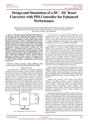
Power Supply Design Seminar 2016/17Learn about the basic design guidelines forbidirectional DC/DC converters in hard- andsoft-switching modes.A bidirectional direct current (DC)/DC converter is a key element of many newapplications, such as automotive, server and renewable-energy systems. Low-voltagebidirectional DC/DC converters are usually nonisolated. All bidirectional converterdesigns or products currently on the market are based on the hard-switchingsynchronous buck topology. This paper uses an automotive 48-V/12-V bidirectionalconverter as an example with which to revisit the hard-switching synchronous bucktopology and compare it to the transition-mode totem-pole zero-voltage-switching(ZVS) topology.We used a digital controller to implement both hard- and soft-switching controls. Aunique ZVS transition-mode control synchronizes multiple phases and maintains deadtime cycle by cycle. We also designed and optimized two 110-A DC/DC convertersfor each topology in order to compare their performance, including efficiency andelectromagnetic interference (EMI). Our results provide a guideline when designingbidirectional DC/DC converters to meet different cost, efficiency and EMI requirements.Introductionhave increased significantly – approaching 3 kW of aMany emerging applications require energy to be12-V power-supply limit.transferable between two ports bidirectionally. TheA mild HEV demands much higher power. Overtwo applications discussed in this paper using200 A of current distributed on a 12-V bus requiresa low-voltage bidirectional DC/DC converter area larger copper-wire cross-section, which increasesa 48-V/12-V automotive dual-bus system and asystem cost. Besides high-current-distributionserver local energy storage (LES) system. Theseconduction loss, 12-V high-power equipmentsystems do not normally require isolation. Forbecomes less efficient and has higher loss withdifferent systems, the reason and purpose forincreasing output power. To solve this issue, a 48-Vusing bidirectional DC/DC converters can be quitepower system is added to power the high-powerdifferent. With more and more electrification incomponents instead. Table 1 shows an example ofautomotive designs, the power demands for start-a BMW micro-HEV power-system change plan [1].stop cars and micro-hybrid electric vehicles (HEVs)Texas Instruments2September 2016
Power Supply Design Seminar 2016/17Table 1. Displacement of high-power loads [1].Table courtesy of BMW.Figure 1. A dual-bus power system for vehicle 12-V loads and 48-V loads.This power-system change plan eliminates thetechnology becomes practical, at which pointalternator and uses a bidirectional DC/DC convertermanufacturers can switch all components to 48 V.powered by a 48-V bus to charge a 12-V batteryFor servers and data centers, LES is a new power(Figure 1).architecture designed to minimize backup-powerA 48-V system has many advantages. For start-footprints and reduce system cost while improvingstop operation, recovering energy during brakingservice availability. Microsoft initially proposed LESor deceleration with 48 V is twice as efficient[6], but other industries quickly adopted it. Insteadwhen compared to 12 V [1], [2], [3], [4], [5]. Theof using a centralized uninterruptable power supplyrecovered energy can provide supplemental power(UPS), LES provides more reliable local backupto accelerate the vehicle, enabling a driving systempower. Figure 2 shows the differences betweento gain fuel efficiency from downsized engines rathera traditional data center and a new data centerthan losing engine performance. A 48-V systemwith LES.also confers the advantages of hybridization withoutThe simplicity of the LES design, coupled with itsthe complexity while boosting overall fuel efficiencycost structure and service model, provide significantby 10 to 15 percent, which will help manufacturersbenefits for data-center deployments. LESmeet increasingly stringent carbon-dioxide emissioneliminates up to 9 percent of the losses associatedtargets. The dual-bus architecture will remainwith conventional UPSs and frees around 25valid until high-energy-density 48-V cold-crankingpercent of facility space.Texas Instruments3September 2016
Power Supply Design Seminar 2016/17topology is a ZVS transition-mode synchronous buckconverter. This topology can operate in ZVS modeand has higher potential efficiency [8], [9], [10], [11].Synchronous buck converters can operate in boostmode when you reverse their output currents.For automotive applications, a multiphaseinterleaving structure avoids the need to use liquidor air cooling, increases the converter’s powercapacity, and distributes heat dissipation across a(a)large area. Unlike a fixed-frequency hard-switchinginterleaved synchronous buck converter, a ZVStransition-mode interleaved buck converter operatesin frequency-modulation mode. You must controlits output inductor’s negative current to limit themaximum switching frequency at light loads andprovide the necessary energy for ZVS operation atheavy loads.All phases must remain synchronized in any(b)operational situation. Optimal and reliable control iscomplicated and still poses significant challengesFigure 2. Traditional data center (a); Microsoft reinvented data center (b).for converter designers. This paper focusesA bidirectional DC/DC converter is also a keyon comparing the control implementation andelement of a server power supply with LES. Whenperformance of the two different topologies. Wepowered by an alternating current (AC)/DC rectifierchose the UCD3138 digital controller for both hard-output, a bidirectional DC/DC converter chargesswitching and ZVS control, and designed a four-LES batteries during normal operation. The LESphase 110-A/12-V power board to operate in bothbatteries provide backup power and regulate thehard-switching and ZVS modes.AC/DC rectifier output voltage in the event of apower outage.Bidirectional DC/DC converters have manyapplications and play an increasingly important role inenergy recovery and power-system management. Themost popular topology used for a converter designis a hard-switching synchronous buck converter, dueto its circuit and control simplicity [7]. The other mainTexas InstrumentsTopology and controlA single-phase bidirectional converter (Figure 3)can operate in buck mode and boost mode withhard-switching or ZVS operation. When Q top is anactive switch and Q bot is a synchronous switch,the converter operates in buck mode (Figure 4);when the roles of Q top and Q bot reverse, theconverter is in boost mode (Figure 5).4September 2016
Power Supply Design Seminar 2016/17Figure 3. A bidirectional converter power stage.Figure 6. Waveforms in ZVS buck mode.Adaptive dead-time control minimizes switchingand body-diode conduction losses. Equation 1calculates the dead time Td off as:Figure 4. Waveforms in hard-switching buck mode.𝑇𝑇𝑇𝑇 𝑜𝑜𝑜𝑜𝑜𝑜 2 𝐶𝐶𝐶𝐶𝐶𝐶𝐶𝐶 𝑡𝑡𝑡𝑡 𝑉𝑉!"𝐼𝐼 𝑝𝑝𝑝𝑝(1)where Coss tr is the equivalent capacitance of ametal-oxide semiconductor field-effect transistor(MOSFET) when Vds swings between 0 and V48,V48 is the voltage on the 48-V bus, and I pk is theactive switch Q top turn-off current.After Q bot turns on, IL starts to decline. The switchstays on until the current reaches the predeterminedFigure 5. Waveforms in hard-switching boost mode.negative current expressed as Equation 2:You can control the same buck converter to𝐼𝐼 ��𝑛𝑛𝑛 achieve ZVS by letting the inductor current becomenegative. When Q top turns on in buck mode(Figure 6), the inductor current, IL, builds up linearly.When Q top turns off, IL discharges switching nodeV SN down. As long as the dead time Td off is2 𝐶𝐶𝐶𝐶𝐶𝐶𝐶𝐶 𝑡𝑡𝑡𝑡 (𝑉𝑉!" – 2 𝑉𝑉!" )𝑇𝑇𝑇𝑇 𝑜𝑜𝑜𝑜(2)where V12 is the voltage on the 12-V bus andTd on is the dead time between when Q bot turnsoff and Q top turns on.long enough, the bottom field-effect transistor (FET)To achieve optimal operation, the dead time Td onQ bot is able to achieve ZVS. However, excessiveshould be half the switch-node resonant perioddead time results in a Q bot body-diode conduction(Equation 3):loss increase. Thus, turn on Q bot as soon as V SNdischarges to zero.Texas Instruments𝑇𝑇𝑑𝑑!" 𝜋𝜋 𝐿𝐿𝐿𝐿 𝐶𝐶𝐶𝐶𝑠𝑠𝑠𝑠!"5(3)September 2016
Power Supply Design Seminar 2016/17The energy stored in the output inductor is then justOne controller has eight digital pulse-widthenough to charge the switch-node V SN up to themodulator (DPWM) outputs (four pairs), which canV48 bus voltage, and Q top can turn on with ZVS.control four phases simultaneously. A shunt resistorZVS operation is also possible when operatingsenses each phase inductor current. All phasein boost mode, as shown in Figure 7. Thecurrents are summed together and connected tosame control ideas apply to the negative-currentEADC0 for current-loop control.calculation and dead-time control.Figure 7. Waveforms in ZVS boost mode.Figure 8. Circuit block diagram of a bidirectional DC/DC converter.For a hard-switching bidirectional converteroperating in continuous conduction mode (CCM),The 12-V and 48-V bus voltages are sensed anduse adaptive dead-time Td off control to achievefed to EADC1 and EADC2 for voltage-loop control.optimal efficiency but keep Td on as small asTwo general-purpose PWMs (PWM0 and PWM1)possible.generate two programmable analog negative-Control implementationThe UCD3138 is a hybrid digital controller madeup of three hardware digital loops and an ARM7microcontroller [12]. The three digital loops canoperate independently or in cascade mode. Thecontroller architecture maintains the precision andhigh speed required for power processing whileproviding flexible power management.A bidirectional DC/DC converter requires three loopcontrols. One is a current loop, and the other twoare the V48 voltage loop and the V12 voltage loop.The controller’s structure and peripherals match thisbidirectional converter application perfectly.Figure 8 shows a circuit block diagram of acontroller-based bidirectional DC/DC converter.Texas Instrumentscurrent references and connect to compactor 1and 2. One reference is for ZVS buck mode andthe other is for ZVS boost mode. The comparatorsdetect the master phase inductor’s negative current.When the current reaches the reference thresholdvalues, the comparator output, which connects tothe UCD3138’s sync pin, becomes high.The rising edge of the signal at synchronous inputforces the controller’s DPWM to restart a newswitching cycle and achieve hardware-basedfrequency modulation. All slave phases follow themaster phase’s frequency cycle by cycle. Each slavephase has a different delay time from the masterphase. The ARM7 can modify the delay time, so allphases can maintain 90-degree interleaving whenthe switching frequency varies.6September 2016
Power Supply Design Seminar 2016/17One important feature of the UCD3138 is thatall dead times remain unchanged regardless ofswitching-frequency changes, while the ARM7 stillhas the privilege and flexibility to modify the deadtime at any point.A bidirectional DC/DC converter benefits fromcurrent-ripple cancellation of the interleavedstructure. Selecting the right phase number canminimize or even fully cancel current ripple. For thisspecific case, where the high-voltage bus is 48 Vand the low-voltage bus is 12 V, the voltage ratio isFigure 9. Current ripple versus the number of phases.Design and test4-to-1. The optimal phase number is thus a multipleTo validate the control scheme and compareof four.topology performance, we designed a 110-A (onFigure 9 shows the normalized current ripple versusthe number of phases. You can see that for an idealcase, the inductor current ripple fully cancels outwhen the phase number is a multiple of four. It is forthis reason that we used a four-phase bidirectionalDC/DC converter to compare performance.the 12-V side) bidirectional DC/DC converter. Whenloaded with a different set of power components,the same design can operate in either hardswitching mode or ZVS mode. Table 2 shows thepower-stage component selection and design, andFigure 10 shows the 110-A bidirectional DC/DCreference design.Table 2. Power-stage component selection and design.Texas Instruments7September 2016
Power Supply Design Seminar 2016/17waveforms, but you can still see some voltageovershoot when the MOSFETs turn off at a largecurrent due to the printed circuit board (PCB) andpower MOSFET pin leakage inductance. Hardswitching operation has a higher voltage overshoot.In addition to the PCB and MOSFET lead leakage,the MOSFET body diode’s reverse recoverycontributes to overshoot and ringing as well.Figure 10. Example of a 110-A (1.6-kW) bidirectional DC/DCconverter.Figure 11 shows the switching-node voltagewaveforms and inductor current waveform whenthe converter operates in ZVS buck mode. Theswitching-node waveforms are clean and soft, witha 90-degree phase offset from each other. Themaximum frequency is clamped to 450 kHz. As theload decreases, the switching frequency increases.Figure 12. Hard-switching buck at 20 A.When the switching frequency reaches the 450-kHzlimit, the negative current increases to prevent theNo overshootswitching frequency from increasing further.Soft on/off edgesFigure 13. Soft-switching buck at 20 A.Fig 13TI Information – Selective Disclosure. HVPS/ Battery Management Deep Dive 2015Redefining the future of power through high voltage – www.TI.com/highvoltage Complete Solutions Robust Design Tools Innovative Products1-4Figure 11. Switching-node voltage and inductor-current waveforms inZVS buck mode.Figures 12 through 19 show the differencebetween hard switching and soft switching. ZVSoperation has softer voltage-rising and falling-edgeTexas InstrumentsFigure 14. Hard-switching buck at 110 A.8September 2016
Power Supply Design Seminar 2016/17Figure 15. Soft-switching buck at 110 A.Figure 18. Hard-switching boost at 110 A.Figure 16. Hard-switching boost at 20 A.Figure 19. Soft-switching boost at 110 A.Figure 20 shows the converter’s bidirectionaloperation. The 12-V current ramps up and downbetween positive and negative values. Whenoperating in buck mode, the current is positive andcharges the 12-V battery. The current becomesnegative in boost mode and the power from the12-V battery charges up the 48-V battery.Figure 17. Soft-switching boost at 20 A.Figure 20. Waveforms of bidirectional operation.Texas Instruments9September 2016
Power Supply Design Seminar 2016/17A graphical user interface (GUI) tool (Figure 21)facilitates circuit debugging and tuning and handlesoperation monitoring (Figure 22).Figure 23. Loss breakdown of hard-switching and ZVS buckconverters at full load.Figure 21. Device GUI for circuit debugging and tuning.Figure 24. Efficiency versus load in buck mode.Figure 22. GUI for bidirectional DC/DC converter operation settingand monitoring.We calculated the power losses of the referencedesign and charted the losses in the columnsshown in Figure 23. You can see that the total lossof the converter with ZVS operation reduces, butthe reduction is not significant. The major changeis the power loss shifting from the MOSFETs tothe inductors. This shift could be advantageous,since magnetic components are more reliable thansemiconductors. Perhaps better magnetic materialscould improve the ZVS converter’s efficiency evenfurther. Figures 24 and 25 plot the converter’sefficiencies versus loads.Texas InstrumentsFigure 25. Efficiency versus load in boost mode.In both buck and boost mode, hard switching hasbetter light-load efficiency, while at heavy loads softswitching becomes more efficient. Soft switchingstill has turn-off loss. When the switching frequencyincreases at light loads, the loss becomes moresignificant.10September 2016
Power Supply Design Seminar 2016/17We conducted additional tests with light-loadmanagement, which showed that disabling thesynchronous FETs or using ideal diode-emulationcontrol improved efficiency substantially. This projectprimarily focused on heavy loads where thermalperformance is the major concern, but real productdesigns need light-load management.Figures 26 through 29 show thermal images atfull loads. We did not use any forced air for cooling,except a breeze from an electrostatic discharge(ESD) ion generator on top of the test bench to helpstabilize the downfacing heat-sink temperature.Figure 28. Hard-switching boost thermal image.From the thermal images, you can see that theMOSFETs’ soft-switching temperature is lowerthan its hard-switching temperature in both buckand boost modes, and the overall soft-switchingtemperature is more even.Figure 29.Soft-switching boost thermal image.EMI is always one of the main concerns whenselecting a topology. To have a reasonablecomparison and better understand EMI behavior,Figure 26. Hard-switching buck thermal image.we used the same EMI filter design on both thehard- and soft-switching converters and scannedthe EMI in buck mode at full load. Test data inFigure 30 indicates that soft switching and hardswitching have no significant EMI difference under1 MHz, but soft-switching’s advantages becomemore substantial when the frequency increases.At 10 MHz and above, soft switching results in asmuch as a 15-dB reduction.Figure 27. Soft-switching buck thermal image.Texas Instruments11September 2016
Power Supply Design Seminar 2016/17Figure 30. Conducted EMI test of bidirectional DC/DC converters in buck mode at full load.Summary and conclusionsLight-load management can improve both soft-We designed and optimized two 110-A bidirectionaland hard-switching light-load efficiency. SoftDC/DC converters to compare performance inswitching does not exhibit a lower conductedhard and soft switching and developed a GUI toEMI emission under 1 MHz, but its advantagefacilitate circuit debugging, tuning and monitoring.becomes more significant with an increase inSoft switching had softer and smoother switching-frequency and reaches 15-dB EMI reductionsnode waveforms and lower voltage overshoot. Withat 10 MHz and above.no light-load management, hard switching is moreSoft switching works better in general, but itsefficient than soft switching at light loads, while softdesign and control are more challenging. Topologyswitching has better efficiency at heavy loads.selection for a design would depend on the specificThe efficiency advantage of soft switching at heavyrequirements and the time and resources available.loads is not significant due to its large peak currentand high turn-off loss, but its shift of losses fromsilicon to magnetic parts results in lower MOSFETtemperatures and more even thermal distributionacross the power board.The UCD3138 was a good fit for both the hardand soft-switching bidirectional DC/DC converterdesigns. Its hybrid architecture offers precise andfast hardware power-processing control and flexiblesoftware power management. The controller’shardware can support multiphase ZVS frequencymodulation and maintain a constant dead time.Texas Instruments12September 2016
Power Supply Design Seminar 2016/17References8. Zhang, J. “Bidirectional DC-DC Power Converter DesignOptimization, Modeling and Control.” PhD diss, Virginia1. Sirch, O. “48 Volt – its threats and opportunities.”Polytechnic Institute, 2008.Automotive 48 V Power Supply Systems 2013 InternationalConference, Nov 12-14, 2013.9. Liqin, N., D.J. Patterson, and J.L. Hudgins. “High PowerCurrent Sensorless Bidirectional 16-Phase Interleaved2. Harrop, P. “48 V vehicle systems becoming significant.”DC-DC Converter for Hybrid Vehicle Application.” IEEEIDTechEx, Aug. 12, 2015.Transactions on Power Electronics 27, No. 3 (2012)3. “48V: Collected facts, latest developments and expert1141-1151.opinions.” Paper presented at 3rd International ConferenceAutomotive 48 V Power Supply Systems 2015,10. Yu, W., and J.S. Lai. “Ultra High Efficiency BidirectionalDC-DC Converter with Multi-Frequency Pulse WidthNov. 24-26, 2015.Modulation.” Twenty-Third Annual IEEE Applied Power4. “48V Technology on the Automotive Horizon.”Automotive IQ report presented at the 3rd InternationalElectronics Conference and Exposition (APEC) (2008)Conference Automotive 48 V Power Supply Systems 2015,1079-1084.Nov. 24-26, 2015.11. Sah, A., K. Chaudhary, and V.V. Ratnam. “Non-IsolatedMultiphase Buck-Boost Converter Design for Electric5. Els, P. “48 Volt Electrification: The next step to achieving2020 emissions.” Paper presented at 3rd InternationalVehicle Applications.” 2014 Annual InternationalConference Automotive 48 V Power Supply Systems 2015,Conference on Emerging Research Areas: Magnetics,Nov. 24-26, 2015.Machines and Drives (AICERA/iCMMD) (2014) 1-6.6. Harris, S. “Microsoft Reinvents Datacenter Power Backup12. UCD3138 Highly Integrated Digital Controller for Isolatedwith New Open Compute Project Specification.” MicrosoftPower. Texas Instruments data sheet (SLUSAP2F),Server & Cloud Blog, March 10, 2015.November 20137. Waffler, S., and J.W. Kolar. “Efficiency Optimization of anAutomotive Multi-Phase Bi-directional DC-DC Converter.”2009 IEEE 6th International Power Electronics and MotionControl Conference (IPEMC 2009) 574-581.Texas Instruments13September 2016
TI Worldwide Technical SupportInternetTI Semiconductor Product Information CenterHome Pagesupport.ti.comTI E2E Community Home Pagee2e.ti.comProduct Information CentersAmericas Phone 1(512) 0-7544FaxInternet/Email 1(972) 927-6377support.ti.com/sc/pic/americas.htmEurope, Middle East, and AfricaPhoneEuropean Free CallInternationalRussian Support00800-ASK-TEXAS(00800 275 83927) 49 (0) 8161 80 2121 7 (4) 95 98 10 701 Note: The European Free Call (Toll Free) number is not active inall countries. If you have technical difficulty calling the free callnumber, please use the international number above.FaxInternetDirect Email (49) (0) 8161 80 rnationalDomestic co.jp/picAsiaPhoneToll-Free Number Note: Toll-free numbers may not supportmobile and IP phones.Australia1-800-999-084China800-820-8682Hong New 6-0010International 86-21-23073444Fax 86-21-23073686Email tiasia@ti.com or htmImportant Notice: The products and services of Texas InstrumentsIncorporated and its subsidiaries described herein are sold subject to TI’sstandard terms and conditions of sale. Customers are advised to obtain themost current and complete information about TI products and servicesbefore placing orders. TI assumes no liability for applications assistance,customer’s applications or product designs, software performance, orinfringement of patents. The publication of information regarding any othercompany’s products or services does not constitute TI’s approval, warrantyor endorsement thereof.A021014The platform bar and E2E are trademarks of Texas Instruments. All other trademarksare the property of their respective owners. 2016 Texas Instruments IncorporatedPrinted in U.S.A. by (Printer, City, State)SLUP342
IMPORTANT NOTICETexas Instruments Incorporated and its subsidiaries (TI) reserve the right to make corrections, enhancements, improvements and otherchanges to its semiconductor products and services per JESD46, latest issue, and to discontinue any product or service per JESD48, latestissue. Buyers should obtain the latest relevant information before placing orders and should verify that such information is current andcomplete. All semiconductor products (also referred to herein as “components”) are sold subject to TI’s terms and conditions of salesupplied at the time of order acknowledgment.TI warrants performance of its components to the specifications applicable at the time of sale, in accordance with the warranty in TI’s termsand conditions of sale of semiconductor products. Testing and other quality control techniques are used to the extent TI deems necessaryto support this warranty. Except where mandated by applicable law, testing of all parameters of each component is not necessarilyperformed.TI assumes no liability for applications assistance or the design of Buyers’ products. Buyers are responsible for their products andapplications using TI components. To minimize the risks associated with Buyers’ products and applications, Buyers should provideadequate design and operating safeguards.TI does not warrant or represent that any license, either express or implied, is granted under any patent right, copyright, mask work right, orother intellectual property right relating to any combination, machine, or process in which TI components or services are used. Informationpublished by TI regarding third-party products or services does not constitute a license to use such products or services or a warranty orendorsement thereof. Use of such information may require a license from a third party under the patents or other intellectual property of thethird party, or a license from TI under the patents or other intellectual property of TI.Reproduction of significant portions of TI information in TI data books or data sheets is permissible only if reproduction is without alterationand is accompanied by all associated warranties, conditions, limitations, and notices. TI is not responsible or liable for such altereddocumentation. Information of third parties may be subject to additional restrictions.Resale of TI components or services with statements different from or beyond the parameters stated by TI for that component or servicevoids all express and any implied warranties for the associated TI component or service and is an unfair and deceptive business practice.TI is not responsible or liable for any such statements.Buyer acknowledges and agrees that it is solely responsible for compliance with all legal, regulatory and safety-related requirementsconcerning its products, and any use of TI components in its applications, notwithstanding any applications-related information or supportthat may be provided by TI. Buyer represents and agrees that it has all the necessary expertise to create and implement safeguards whichanticipate dangerous consequences of failures, monitor failures and their consequences, lessen the likelihood of failures that might causeharm and take appropriate remedial actions. Buyer will fully indemnify TI and its representatives against any damages arising out of the useof any TI components in safety-critical applications.In some cases, TI components may be promoted specifically to facilitate safety-related applications. With such components, TI’s goal is tohelp enable customers to design and create their own end-product solutions that meet applicable functional safety standards andrequirements. Nonetheless, such components are subject to these terms.No TI components are authorized for use in FDA Class III (or similar life-critical medical equipment) unless authorized officers of the partieshave executed a special agreement specifically governing such use.Only those TI components which TI has specifically designated as military grade or “enhanced plastic” are designed and intended for use inmilitary/aerospace applications or environments. Buyer acknowledges and agrees that any military or aerospace use of TI componentswhich have not been so designated is solely at the Buyer's risk, and that Buyer is solely responsible for compliance with all legal andregulatory requirements in connection with such use.TI has specifically designated certain components as meeting ISO/TS16949 requirements, mainly for automotive use. In any case of use ofnon-designated products, TI will not be responsible for any failure to meet dioAutomotive and fier.ti.comCommunications and Telecomwww.ti.com/communicationsData Convertersdataconverter.ti.comComputers and Peripheralswww.ti.com/computersDLP Productswww.dlp.comConsumer ergy and Lightingwww.ti.com/energyClocks and wer Mgmtpower.ti.comSpace, Avionics and ollersmicrocontroller.ti.comVideo and Imagingwww.ti.com/videoRFIDwww.ti-rfid.comOMAP Applications Processorswww.ti.com/omapTI E2E Communitye2e.ti.comWireless Connectivitywww.ti.com/wirelessconnectivityMailing Address: Texas Instruments, Post Office Box 655303, Dallas, Texas 75265Copyright 2016, Texas Instruments Incorporated
A bidirectional direct current (DC)/DC converter is a key element of many new applications, such as automotive, server and renewable-energy systems. Low-voltage bidirectional DC/DC converters are usually nonisolated. All bidirectional converter designs or products currently on the market are based on the hard-switching synchronous buck topology.