Transcription
1EE2 ARM Experiment: PCB DesignTutorialVersion:2.168Date:January 13, 2016Learning Objectives Understand the basic layered structure of a PCB.Understand the affect of designrules in the design process.Be competent at designing a simplePCB using Altium Circuit Maker.Be aware of some of the trade-offswhen laying out a PCB.Deliverables Gerber File Deadline: 22/01/2016,14:00 Marking: Questions Unmarked, Afunctioning PCB will be a positivein SWITCHI. I NTRODUCTIONThis section of work is designed to introduce you the fundamentals of PCB design. The design that you will produce inthe next two lab sessions will be used inthe Summer term SWITCH experiment; awell designed board could save you lots ofdebugging headaches! Your completed designwill be an embedded computing platform witha microprocessor module, an OLED displayand four touch switches.This lab work will make use of theEDA (Electronics Design Automation) pack-age called Altium CircuitMaker, which hassimilar functionality to the widely-used Altium Designer. CircuitMaker is free to use andyou may find it useful for future personal andacademic projects.II. W HAT IS A PCB?A PCB or Printed Circuit Board is amethod of mounting and connecting manycomponents together. It consists of a structural layer, usually made from a glass fibrecomposite, and a number of conducting andinsulating layers on both sides. For this experiment we will have one conducting layerand one insulating layer on each side, butmore complex designs can use many more.The conducting layer is made from copperand sits adjacent to the structural layer; tracks,solder pads and other features can be madein this layer by etching away sections to giveisolated areas of copper. The conductive layeron the top can be connected to the conductivelayer on the bottom by plated through holes(PTH), or vias, which are drilled holes that arethen coated in conductive material. By usingboth layers and vias to connect between themcomplicated wiring can be achieved withoutany external wires being used.After the conductive layers have beenetched and vias added an insulating layeris added on top to avoid shorting, this isusually the characteristic green colour youwill have noticed on most PCBs. This is donevia a silk screen process. Optionally a finalcosmetic layer on both sides can be added
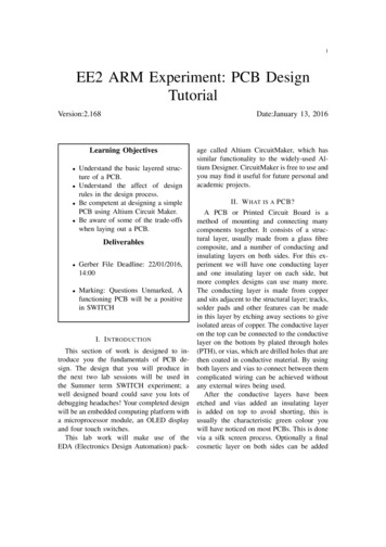
start with a partially set up project to savetime, this is done by ‘forking’ an existingproject. ‘Forking’ refers to making a copyof an existing project that is editable andowned by you. Go to ‘Open Project’ then inthe search box type ‘PCB Lab’. Select theproject created by Edward Stott, and click on‘Fork’, rename the project to your groupname and make it a ‘sandbox’ project,this makes it private until you are ready torelease the design, a good would be NAMEEEE TOUCHSWITCH, where NAME is yourname. On your new project click ‘open’ (noton the schematic!) to open the project, theschematic file and PCB layout will now beavailable on the left hand side of the screen.which is usually referred to as ‘the Overlay’.This usually has small white numbers indicating the components that should be placedin particular places, version numbers of theboard and other identification marking. SeeFigure 1 for a demonstration of these differentlayers.Research: How are PCBs constructedwith more than two copper layers?Task 1: Register for CircuitMaker andfork the PCB Lab project (changing thename of the project and making it a‘sandbox’ project).Fig. 1: A complete PCB, silver rings are viasconnecting to the other side, dark green linesshow where the copper was etched away toform tracks to carry the signals. The greencovering prevents short circuits. The whitewriting is a reference to help with construction.IV. P RODUCING A S CHEMATICProducing a working PCB first requiresa correct electrical description of the circuityou wish to build. This is the function of aschematic, it shows what components are tobe used and how they are connected together.Your project already contains a partiallycomplete schematic; double-click on it toopen the schematic editor window. You willfind the microcontroller module, OLED display and touch pads already placed. You willneed to fill in the missing connections andadd the circuitry to detect when the pads aretouched.The touch pads work by building an R-Coscillator. When the pad is touched, the finger introduces extra capacitance and the frequency of the oscillator reduces. The microprocessor will count the oscillator frequencyand applies a threshold to decide if the padis being touched or not. The circuit for theoscillator is shown in Figure 2.III. S ETTING U P A LTIUM C IRCUIT M AKERAltium Circuit Maker uses cloud servicesfor data storage and project management anda local piece of software to run the userinterface. To use it, you must first register foran account by following the instructions here:http://www.circuitmaker.com/#download LabPCs already have CircuitMaker installed soyou can start the software and log in with yournew account. If you want to install the software on your own PC follow the instructionsin your registration confirmation email. Macand Linux users will need to use a Windowsvirtual machine. For this experiment you will2
Task 2: What values should be used for Rand C in Figure 2? Aim for the oscillatorfrequency to be 100kHz normally and50kHz when the pad is pressed. Assumethe touch pad capacitance is 10pF and itincreases to 50pF when is touched.use U for ICs and other relevant componentsare listed in in Table I. The other componentsthat you will need for this design are given inTable II.To connect components together use the‘wire’ tool (hotkey ‘w’). Your final designshould look like Figure 3. Use the ‘Powerports’ tool too add symbols such as ‘GND’and ‘VCC’ and for long connections, such theones between the output of the oscillators andthe Mbed, net labels are useful to keep theschematic neat and easy to read. It is usefulto use the ‘Electrical Rules Check’ located inthe ‘Outputs’ tab, this will list a variety of errors. You will have some errors regarding thepower supply pins on the SN74HC14D, thesecan be safely ignored. Another convinientshortcut is the ‘space’ key when moving partsmakes the selection rotate by 90 degrees, ifthe part is highlighted it will rotate around theorigin.The core of the oscillator is a Schmitttrigger inverter and there are six of these ina SN74HC14D, which is a standard logicintegrated circuit. If you click on the tab‘Libraries’ on the far right hand side of theinterface a new sub-window will open. In thefirst drop down box select ‘Octopart’, whichis the large open source component library.In the search box enter ‘SN74HC14D’, thefirst result should be an exact match, the otherresults are very similar chips with differentpackages. The first result should also have asmall cube icon above the image, this indicates that the part has a footprint, 3D model orsimulation model attached. If the componentis lacking this then you would need to createthese yourself.Task 3: Draw four oscillator circuits, onefor each touch pad. What should youdo with the two unused inverters in theSN74HC14D?Research: The component library in CircuitMaker is ‘crowd-sourced’. What arethe pros and cons of this approach? Howwould you create your own custom component? How would a component librarybe managed in industry?Task 4: Connect the oscillator outputs tothe OM11043 and complete the wiringto the OLED display. The display iscontrolled with an SPI bus. Which pinsshould you use on the OM11043 forthese signals?Select the first SN74HC14D listing, thenunder ‘Revisions’ pick the entry by ‘Edward Stott’ now you can select the throughhole package from the shown footprintimages (the last one). Now click ‘Place’,then press ‘tab’ and change the designatorfrom ‘U?’ to ‘U3’, now place the IC on theschematic sheet, make sure you place all 6sub parts!. The ‘U3’ is called a designatorand it uniquely identifies each physical component (U3 is represented on the schematicby the six sup-parts U3A–U3F). It is usual toThe circuit in Figure 3 is lacking decoupling capacitors. Decoupling capacitors arenecessary to prevent noise from being transferred between components via their powersupplies.Task 5: Add decoupling capacitors to thecircuit as appropriate.3
Fig. 3: The complete schematic to be capturedTABLE I: Typical designatorsComponent TypeIntegrated gnatorURCJLDTABLE II: Components used in this designComponentCapacitorResistorSchmitt InverterFig. 2: One unit of the Schmitt trigger oscillator, 4 of these will be required for the finisheddesign.Search termK104K15X7RF5TL2CFR16J470RSN74HC14Dbering.V. AUTOMATIC A NNOTATIONTask 6: Annotate the schematic.At this point most of the componentswill be designated in the form ‘C?’ and‘R?’. These can be automatically enumerated by clicking ‘Tools’, ‘Annotation’, ‘Annotate Schematics Quietly’. It is possibleto re-annotate the schematic using ‘AnnotateSchematic’, it should propose sensible num-VI. P ERFORMING E LECTRICAL RULESC HECKNow that you are comming to the end ofthe schematic capture it is very important tocheck for inconsistencies. Clicking on ‘Electrical Rules Check’ under the ‘Outputs’ tab4
will generate a list of warnings and errorsexhibited in your schematic. Some warnings,and at times errors, can be tollerated; youmust judge which can be ignored. Good questions to ask are: Would this make the PCBfail? Would this make the design unclear tosomeone looking through it for the first time?You should perform ERC regularly throughthe process of designing a PCB to catch errorsearly before they become difficult to fix.rules would usually be set by the manufacturing constraints provided by the PCBfabrication facility. Your project is already setup with fairly conservative rules to make iteasier to solder, but click on ‘Design Rules’in the ribbon to see the kinds of rules that areavailable. This is very important when youwork on a large design, as the designer willnot have the ability to manually check thateverything on the board is sensible.VII. PCB L AYOUTOnce you are happy with the schematicyou have generated, you are ready to designthe physical PCB layout. There is a templatePCB already in the project, double click itto open the PCB editor window. You cannow import all the parts from the schematic.Goto the ‘Home’ tab then click ‘Project’ - ‘Import Changes from .’, then execute thechanges. All your components should nowbe displayed. Click and drag them into yourpreferred arrangement, using the space key torotate. To help you visualise the PCB you canpress the ‘3’ key to enter 3D mode, press ‘2’to re-enter the 2D view. Tips for arrangement: Parts with many pins should not be veryclose to the edge to allow for tracks toescape the area. Parts that are electrically connected together, generally should be near eachother to minimise track length. Thestraight ‘rat’s nest’ lines give an indication of the wires you’ll need to create solook out for many crossing lines. Have all of the touch switches near theedge so they can be touched easily. Usethe 3D view to help visualisation.Research: What is a typical minimumwidth for a copper track and minimumgap between tracks on a commercialPCB?B. RoutingRouting is the process of connecting thecomponents using tracks. There are 2 mainways to do this, automatically and manually.Automatic is very useful to check if thedesign is easy to route, if it succeeds there arelikely many different routing arrangementsthat will work, this is good! Though dokeep in mind that a skilled human will findbetter routing strategy than the auto routing.Also the autorouter could make decisions thatmake the board function less well than if acareful designer added the tracks, for examplekeeping different high frequency tracks awayfrom each other.Try the autorouter first by clicking the‘Tools’ tab, ‘Autoroute’, ‘All’. If your positioning of the components was reasonablethen it should complete without errors andwithout the need for additional vias. Try themanual routing also. First clear the autorouteby going to the ‘Home’ tab, ‘Unroute’, ‘All’.Then using the ‘Route’ button you can clickon signals and connect them with tracks. Thetracks will automatically move other tracksout of the way. To add a via on the trackpress the ‘2’ key. To change the layer you arerouting on press the ‘L’ key. You can eitherTask 7: Arrange parts on PCB.A. Design RulesThis software provides a system for checking your design against a set of rules. The5
this?continue this process or reuse the autoroutetool.VIII. F INAL T OUCHESTask 8: Route the PCB. Which wiresmight be sensitive to noise and whichwires might emit noise? Try to keep theseapart.1) Add Group Name: Using the text tool,add your group name to the top overlay.Use the ‘tab’ key to change layers and otherparameters of the text.2) Arrange Designators: Move and reorientate the component designators so that theyare logically placed around the components.Remember they won’t be visible underneathcomponents! Any overlay that lies on topof component pin pads will be removed atmanufacture.C. Polygon FillNow that your PCB is routed it wouldfunction correctly if it were to be manufactured, though the board in this state isvulnerable to interference due to the lack ofan adequate ground plane. Also the amountof copper that must be removed is very largeand will use lots of etchant, which is bad forthe manufacturer, the environment and for thecost of the boards to produce. The solution toboth of these problems is to add a copper fillthat is tied to the GND signal. We will needone on both sides of the board.To add a polygon fill, select the ‘PolygonPour’ button, a dialogue box will appear. Giveit a name such as ‘Top GND’. Select the layeras ‘Top Layer’. Connect to net ‘GND’. Usethe drop down box to select ‘Pour over allsame net objects’, and select ‘Remove DeadCopper’. After pressing ‘OK’ you will be ableto place the boundary lines of the copperpour along the board outlines (the fill willautomatically be trimmed back according tothe design rules). Setting a course grid maymake this easier. Do the same for the bottom.Use the combination of ‘shift’ ‘space’ tochange the cornering style. Use ‘Escape’ keywhen finished and the pour will be added.Task 10: Finalise the top overlay.IX. D ESIGN RULES C HECKWhen producing batches of PCBs it isimportant that they meet the design rules thatyou looked at in Section VII. To run a checkclick the ‘Design Rules Check’ button, run thecheck with the default settings, this will bringup a summary of your warnings. Some ofthese are more critical than others, to see thesource of an error scroll down and click on theerror instance. Some errors may not be easilyremoved, make a decision whether you needto correct them or not. Anything regarding thesilk layer will not affect the operation of theboard, so use the 3D view to check if the silkscreen is good enough for your purposes. Unrouted errors and clearance errors will affectthe board operation and should be corrected.Task 11: Review the results of the designrules check.Task 9: Add copper fills to the PCBX. D ESIGN E XTENSIONSResearch: Notice that the pads that werealready connected to ground now havesmall connections to the ground planeinstead of flooding over them; why isDuring debugging and testing of this circuityou are likely to need to probe signals. Youcould use a header to give you a row ofholes to probe, try finding a 6 pin header6
final submission for this section. You cancheck that the files were generated correctlyby using an online gerber viewer, such ashttp://www.gerber-viewer.com/.with 2.54mm spacing in the parts library,similarly to how we imported componentsin Section IV. Alternatively you can do itdirectly in the PCB editor by adding pads connected to the signal of interest (press tab whenin the pad tool and set the net, remember toroute to it). You can add words to the silkscreen layer using the string tool in the PCBeditor, check your results using the 3D view.Recommended test points: Vcc GND Output 1 Output 2 Output 3 Output 4Final Check: Schematic shown in Figure 3 isfully implemented. The two redundant Schmitt invertersare explicitly added to the schematicand dealt with appropriately. All designators are unique. The ERC passes with only well understood warnings. The PCB is synchronised with theschematic. The board size has remained unchanged from the original size. All of the signals are routed (nomore air wires). There is a polygon fill connected to‘GND’ on both sides of the board. Your group name is on the overlay. Your gerber files and schematic aresubmitted on LabWeb.Task 12(optional): Add a test header.XI. M ANUFACTURING O UTPUTSWhen all of the above is complete and youare happy with the design we must create filesfor the manufacturer to use to produce theboards. These are the Gerber and Drill files.To produce these click ‘Project’, ‘GenerateOutputs’. Save and commit your work whenprompted. A dialogue of all possible outputswill appear, spend a minute looking throughthem. Select ‘Gerber Files’ and ‘NC DrillFiles’. Configure the Gerber files. Go to the‘Layers’ tap and select ‘Plot’ for all of thefollowing layers: Top Overlay Top Solder Top Layer Bottom Layer Bottom Solder Bottom Overlay OutlinePressing ‘Generate’ will start the generation of the files, it will then offer for youto save a zip file containing all of the outputs, this is the file you should give as yourTask 13: Produce the manufacturing filesfor your PCB and submit them on LabWeb.7
name. On your new project click 'open' (not on the schematic!) to open the project, the schematic file and PCB layout will now be available on the left hand side of the screen. Task 1: Register for CircuitMaker and fork the PCB Lab project (changing the name of the project and making it a 'sandbox' project). IV. PRODUCING A SCHEMATIC