Transcription
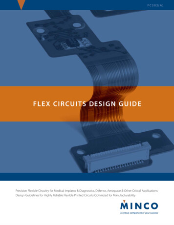
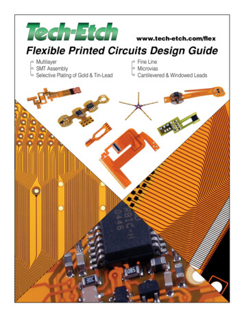
www.tech-etch.com/flexFlexible Printed Circuits D esign GuideMultilayerSMT AssemblySelective Plating of Gold & Tin-LeadFine LineMicroviasCantilevered & Windowed Leads
SINGLE LAYER FLEX CIRCUITSOLDER ACCESS HOLEMATERIALSCONDUCTORCopper is the most commonly used material forcircuit traces and offers the most cost effectivesolution. Thickness typically ranges from .0007"to .0028". Tech-Etch works with both adhesivebased and adhesiveless substrate materials.In addition, Tech-Etch has the capability tomanufacture circuits from specialty metals tosupport specific applications. Some examplesare stainless steel for corrosion resistance,BeCu for spring properties, Cupronickel for highresistance applications, and selective tungstensegments when radiopacity is desired.POLYIMIDE COVERLAYADHESIVECOPPER CONDUCTORDOUBLE LAYER FLEX CIRCUITPOLYIMIDE SUBSTRATESOLDER ACCESS HOLEPOLYIMIDE COVERLAYFOUR LAYER FLEX CIRCUITADHESIVESOLDER ACCESS HOLECOPPER LAYER 1COPPER LAYER 2POLYIMIDE COVERLAYPLATED COPPER THROUGH HOLEADHESIVEPOLYIMIDE COVERLAYADHESIVELESS POLYIMIDE SUBSTRATEINSULATORPolyimide film is the most common insulatormaterial used for flex circuits. Tech-Etch usesthis film as the base layer on single metal layerflex circuits and for inner layers of multilayercircuits.COPPER LAYERSPLATED COPPER THROUGH HOLEPOLYIMIDE COVERLAYPLATEDTHROUGH VIASTech-Etch can provide circuits with platedthrough vias. A via is a metalized throughhole that connects the conductive layers of aflexible circuit.THROUGH VIABLIND VIATech-Etch can also produce blind vias wherethe via connects an outer layer with an innerlayer, but does not go all the way through thecircuit. Buried vias connect internal layers, butalso do not connect to the outer layers. Theseadvanced via types can help increase spacewithin the circuit for other features such ascomponent pads or additional trace routing.Tech-Etch has the ability to drill vias as smallas .001" diameter using laser drill technology.Reference Capabilities Matrix for via sizelimitations.BURIED VIAt Actual SizeCOVERLAYERThe coverlay is the insulating layer placedover the exposed conductors. It is typicallyconstructed of a pre-cut piece of polyimidefilm laminated over the conductors using eitheracrylic or epoxy adhesive.For high density applications Tech-Etch alsohas the ability to work with Photo ImageableCoverlayer. This material is coated over theconductors and does not require adhesive orlamination. Though not as resilient as polyimidefilm, it does support very small and denseaccess openings required by many of today’selectronic components.t Actual SizePhoto Imageable Coverlayer can be tinted witheither amber or green pigment as shown onthe adjacent parts.2
FINISHExposed pads will typically need a finishfor corrosion resistance or compatibilitywith the assembly process or application.Electroplating is the most common finishingprocess. However, it can only be accomplishedwhen all the conductors are connected toa common external bus during fabrication.Tech-Etch offers in-house electroplating ofTin, Tin Lead, Copper, Nickel, Soft Gold, andHard Gold.Windowed LeadsBeryllium Copper CircuitsFor designs where the traces cannot be bussedinto the panel, electroless finishing optionssuch as hot air solder leveling, immersion goldover electroless nickel (ENIG), and immersiontin are available as alternatives.Stainless Steel CircuitsTech-Etch flex circuits can be made RoHScompliant by selecting the proper finish. Ourproduct engineers can help ensure the finishselected supports the intended application.STIFFENERSFR-4 StiffenerStiffeners are added to rigidize areas of acircuit to strain relieve component attachmentlocations, provide a firm surface for mounting,or increase thickness of the circuit tocorrespond to the mechanical specifications(e.g. ZIF connector).Polyimide film is used when the additionalthickness required is .002"-.009". Polyimidestiffeners can have coincidental edges to thecircuit outline.Polyimide StiffenersMolded Plastic StiffenerFR-4 is used when the additional thicknessrequired is greater than .010". The stiffenerfeatures are typically smaller than thecorresponding circuit features by .015".Other materials such as metal or moldedplastic components can also be used asstiffeners for specific design requirements.OUTLININGBGA Pad ArrayTech-Etch has many different options fordefining the circuit outline. Our productengineers will advise on the most cost effectivesolution based on required tolerances andfeature sizes.Tolerance on overall size and the minimumdistance to the nearest copper feature aretwo of the measurements Tech-Etch considerswhen determining whether to use a Steel RuleDie or a Class ‘A’ Hard Tool. All hard tools arefabricated in house to our exacting standards.For extremely small or tight toleranceapplications, Tech-Etch has the capability tolaser cut the outline.3
ASSEMBLY / TESTMECHANICALPROPERTIESOptimum SizesTech-Etch provides circuits up to 16" long.Multi-layer circuits up to 6 conductivelayers are available. Consult factory forlarger sizes.ShieldingFor designs requiring shielding, additionallayers of copper can be added in solid orgrid patterns. Conductive ink shield layersare also available.Tech-Etch offers value added assembly to provideturnkey solutions. Surface mount componentpackage sizes down to 0201 and leadedcomponents down to .4mm pitch are attachedusing our automated pick & place equipment.Tech-Etch also offers through hole componentassembly as well as Single Point or Bar bondingfor applications requiring significant processcontrol for specialty components such as axiallead thermistors, piezo elements, wound coilantennas, and circuit pins.FlexibilityDynamic regions on a Flex Circuit shouldbe identified on the print to allow formanufacturing features that will enhancedynamic performance. The following aregeneral guidelines that apply to nondynamic applications where bends are forinstallation only.Actual SizesMin. Bend RadiusSingle Layer Circuit .10x thicknessMulti-Layer Circuit. .20x thicknessTemperatureMost often the adhesive used is thelimiting factor for high temperature ratingcontinuous service. Typical values are105C (221F) for epoxy adhesive and 120C(248F) for acrylic adhesive. Both systemswill withstand normal soldering practicesafter a moisture driving bake.ENGINEERINGSUPPORTAt the onset of your project we recommendthat you contact Tech-Etch with a preliminarysketch for quotation and feedback onmanufacturability. Our engineers canprovide design assistance to ensure acost-effective production part. We canaccommodate almost any file format such asDWG, DXF, Gerber, Pro-E, and Solid Works.CAPABILITIES MATRIXCircuit Layer Design GuidelinesAttributeABCDEFGHILine Width – Outer LayersLine Width – Inner LayersLine to Line Space – Outer LayersLine to Line Space – Inner LayersPTH Diameter – DrilledPTH to PTH Pitch – Center to CenterPTH Pad Diameter – Outer LayerPTH Internal Land Dia. – Inner LayersPTH Clearance Dia. – Inner LayersACNominalMinimumPreferredDetailG.0015".002" .001".002" .0015".002" .001".002" .001" minø .0065" ø .0075" ø .002"ø .003" ø .002"ø .003" ø .004"ø .005" BFOuterInnerDInnerOuterEHCoverlayer Design GuidelinesPolyimide Coverlay Photo Imageable CoverlayNominal ToleranceFeature SizeRegistrationMin.008"-Pref.020"-Min. .001" .005"Pref. .010" .010"Nominal ToleranceMin.003"-Pref.006"-Min. .001" .001"Pref. .002" .002"If your design requirements exceed the capabilities stated above, please contact the factoryto see if an alternate process or tooling are available.4
MARKETSTech-Etch has specialized in the manufacture of high reliability flexible printed circuits for over 40years. Our focus is on customer service and manufacturing Flex Circuits to your exact specifications.We have a proven history of providing value engineering support and supplying engineered solutionsto customers in the most demanding applications. Flex Circuits manufacturedby Tech-Etch can be found in Medical, Implantable,Telecommunications, Industrial, and otherhigh reliability Electronics applications.FLEXIBLE CIRCUIT SPECIALTY PROCESSINGPolyimide EtchingBy using our uniquepolyimide etchingtechnology, Tech-Etchcan supply circuits withconductors suspendedacross an open windowin the polyimide film orcantilevered from the edgeof the circuit. For circuitsmade with berylliumcopper, cantilevered leadscan be formed and used asintegral contacts.Selective PlatingBy combining our in-houseelectroplating and precisionimaging capabilities, TechEtch can provide circuits withselective finish plating. Thisprocess allows for differentfinishes plated on separateareas of the part. This isparticularly useful whenmultiple assembly processeswill be used (e.g. solderassembly and wire bond).Additive ProcessTech-Etch uses bothSemi-Additive andSubtractive processingtechniques to manufacturetrace patterns. Startingwith copper as thin as 2microns and selectivelyplating copper up to 1oz. thick on adhesivelesspolyimide substrates,Tech-Etch can producefine line circuits with trace and space patternsas small as .001" in production volumes.Contoured CircuitsBy capitalizing on ourexperience with thick metaletching, Tech-Etch can supplyContoured Circuits with integralcontact fingers up to .010"thick. The remaining metal inother areas of the circuit isetched down to approximately.004" thick. Particularlyuseful for applications wherecurrent carrying capacity is arequirement, this process also supports raised solder pads above thecover layer or circuits manufactured on material as thick as .020".5
A TOTAL CAPABILITYWorld Technology LeaderTech-Etch manufactures precision parts for the medical device and equipment, military/aerospace, electronic, telecommunications,and measurement and control industries. Using the latest etching, metal fabrication and metal finishing equipment, Tech-Etchspecializes in photo etching, forming and laminating engineered components, in addition to flexible circuits. The company has along history of technological innovation, quality products, excellent customer service, and growth. From its beginnings as a researchfirm in 1964, Tech-Etch has expanded its product offerings, acquired new businesses, and constructed new facilities. Tech-Etchoperates three manufacturing facilities and has over 500 employees. Corporate headquarters and most of the custom engineeringand manufacturing are located in Plymouth, MA, just 40 miles south of Boston. Over 190,000 square feet of floor space, conferenceand training rooms, and state-of-the-art chemical processes and equipment make this Tech-Etch’s centerpiece. The other facilitiesare located in Fall River, Massachusetts and Litchfield, Minnesota.Wide Range of ProcessesTech-Etch performs a wide variety of processes, and this single-source capability enables it to assume total responsibility for thequality and delivery of our precision products. In-plant services include photo etching and chemical milling, artwork generation andphototooling, stamping from coil stock and forming from etched blanks, tool and die making, production heat treating, flexible circuitdesign and production, welding and soldering, metal finishing, plating, and laser cutting. Secondary operations such as solderingjoints to seal seams, spot welding, and the application of pressure sensitive tapes and insulation materials are also available.ISO 9001 and AS9100D CertificationTech-Etch operates a Quality Management System that is registered to ISO 9001:2015 and AS9100D. This system is designed tocontrol all business processes from Contract Review through the manufacturing processes to final inspection of product. The systemseeks to identify and eliminate all nonconformities and prevent their recurrence through Corrective Action and Internal Auditingprocedures. Process capability studies are available to guide you on part manufacturability. Additional Products & Capabilities EMI/RFI SHIELDINGTech-Etch designs and manufactures abroad line of standard and custom EMI/RFI shielding products including BeCuand wire mesh gaskets, conductiveelastomers, and board level shielding.Our catalog of standard products isavailable online or in print.BOARD LEVEL SHIELDINGTech-Etch uses cost-saving photo etchingto manufacture Board Level Shieldingcomponents such as custom fences withremovable covers. The photo etchingprocess improves design flexibility,shortens lead times, and eliminates hardtooling costs.Standard and Custom DesignPhotoetching processimproves design flexibilityenabling complex shapeswithout expensive tooling.PHOTO ETCHINGTech-Etch specializes in the manufactureof light gauge parts from a wide rangeof materials. The photo etching processallows us to produce parts with highaccuracy. Forming and value addedfinishing are offered to provide turnkeymechanical parts.PrecisionEngineeredPartsNotoolingcharge forstandarddesigns!Removable CoverBoard LevelShieldingTech-Etch specializes in the designand production of board levelshielding. The photoetching processallows the fabrication of parts withcomplex shapes and features thatare impossible to duplicate by othermethods without expensive tooling.Standard Designs OfferedIn addition to custom board levelshielding, Tech-Etch offers a standardtwo-piece board level shield design.This design incorporates a uniquespring finger style attachmentbetween fence and cover, whichcan be customized to almost anyconfiguration. By using standardforming tools, the cost is not passed onto the customer. The standard designmaterials of brass and tin plating arealways in stock. Consult the factory forother materials and finishes.Standard spring finger between fence and cover offers the designflexibility of a removable cover without expensive tooling. Eliminates the expense of formingtools Improved design flexibility Available with internal dividers formulti-cavity applications No limitation on shape or size Through holes and slots availablefor heat dissipation at no charge Wide range of materials andfinishing options Mounting pin stylesavailable in anyconfiguration Intricate geometrywith no impact ontooling cost Depth etched logosand nomenclature at no charge Soldered or resistance welded seams Prototypes in as few as 5 daysVisit our web site for additional information.www.tech-etch.com/shieldISO 9001:2000REGISTEREDwww.tech-etch.comPhotoetching Laser Cutting Forming FinishingThin Metal Parts Flexible Circuits EMI Shielding GasketsTECH-ETCH, INC., 45 Aldrin Road, Plymouth, MA 02360 TEL 508-747-0300 FAX 508-746-9639 E-MAIL sales@tech-etch.comThe data presented in this brochure is based on testing and to our knowledge is accurate and true. Sinceapplications, test measures, and test procedures may vary, we recommend that users of our productsperform their own tests to assure the suitability of these products for their specific applications.ISO 9001AS9100DREGISTEREDwww.tech-etch.comTECH-ETCH, INC., 45 Aldrin Road, Plymouth, MA 02360 508-747-0300 sales@tech-etch.comLITHO IN USA 1966
4 CAPABILITIES MATRIX Circuit Layer Design Guidelines Nominal Attribute Detail Minimum Preferred Line Width - Outer Layers A.0015" .002" Line Width - Inner Layers B.001" .002" Line to Line Space - Outer Layers C.0015" .002" Line to Line Space - Inner Layers D.001" .002" PTH Diameter - DrilledENGINEERING E.001" min PTH to PTH Pitch - Center to Center F ø .0065" ø .0075"