Transcription
Design BriefHigh ReliabilityFlexible Circuitsfor the Medical Marketplacewww.tech-etch.com
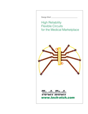
High ReliabilityFlexible Circuitsfor the Medical MarketplaceWindowed LeadsTech-Etch manufacturers high reliability flex circuits used in thediagnostic imaging, patient monitoring, cardiac management and lifescience industries. Flexible circuits provide the thinnest and lightestinterconnect method available. Their extreme thinness makes them verywell suited for dynamic applications where the flex will be in constant orperiodic motion. They contribute to reducing overall system complexityby facilitating assembly and eliminating wiring errors. Flexible circuitswill conform to the available geometry for connections of electronicslocated on different planes within the finished electronic device. Thiscapability is sometimes referred to as 3D packaging.Medical Applications SupportedThe demand for wireless, portable, and more complex electronicassemblies has led to the use of flexible circuits in many high reliabilitymedical applications. Tech-Etch has developed manufacturingprocesses to produce the sophisticated circuits required by theseelectronic devices:Medical Imaging including ultrasound transducers, CT scanners andX-ray scanners. These circuits are typically multilayer microvia circuitsrequiring fine pitch trace / space and precise circuit layer registration.Implanted Devices including cardio defibrillators pacemakers andneurostimulators. These circuits often require telemetry coils, piezoceramic assembly and nickel or niobium terminations.Connector AssemblyMedical Instruments including ultrasonic and phaco surgicalhandpieces. These circuits often require conductor materials other thancopper, such as beryllium copper or stainless steel.Drug Delivery Flex circuits supporting external drug delivery pumpsoften require component assembly which might include a sensor.Increasing Complexity of Medical Flexible CircuitsThe advent of more complex electronic assemblies has driven the needfor high density interconnect circuits. These difficult designs must besourced from very capable flexible circuit manufacturers who are ableto produce multi-layer, fine-line circuits. Tech-Etch will typically use laserdrilling technology to fabricate very small micro vias in addition to laserdirect imaging to generate equally dense circuit patterns. In some casesthese features are so small they cannot be electrically tested using theconventional test fixture process and quality must be confirmed usingmore sophisticated flying probe electrical test process.TEL 508-747-0300 FAX 508-746-9639 sales@tech-etch.com www.tech-etch.com2
Process CapabilitiesA broad array of process capabilities and vertical integration makesit possible to manufacture flexible circuits to the stringent qualitystandards of the medical industry, as well as other high reliabilityapplications:UV Yag Laser6 UV Yag lasers allow for drilled holes down to .001" diameter as wellas prototype and production outlining within .002” of existing copperfeatures.Automated Plated Through Hole ProcessProcess reliability and consistency controlled by automated PTHprocess. Hoist system built by industry leader Integrated ProcessSystems.Laser DrillingLaser Direct Imaging (LDI)Laser direct imaging provides excellent circuit layer registration, with viato pad registration to /-.001" and lines and spaces capabilities down to.001".Additive Copper ProcessingInert anode copper plating supports nodule free copper traces down to.002" trace and space. in 1 oz. thick copper with straight sidewalls.Subtractive Copper ProcessingFine line .001" trace and space on thin copper down to .0005" thickLaser Direct ImagingAutomated Optical InspectionState of the art AOI equipment is used to confirm accuracy of coppergeometry on all work in process.Finishing OptionsSoft Gold, Hard Gold, Nickel, Tin, Tin/Lead, Immersion Silver, ENIG,ENEPIG all available to support assembly process from soldering to wirebonding.Screening and Pick & PlaceAssemblyAutomated SMT assembly using Samsung CP45NEO pick & placedelivers package sizes down to 0201 and 4mm pitch components.Tech-Etch also offers precision single point, bar bonding and handassembly.Circuit Test Standard Opens and Shorts testing per IPC-9252 9252 usingdedicated fixtures. High density bare board testing achieved using flying probe(fixtureless) electrical test. Hipot and Insulation Resistance testing up to 16 channels.Flying Probe Electrical Test Impedance, Inductance and Capacitance bare board testing, as wellas functional in-circuit testing of discrete components (capacitors,resistors, diodes).TEL 508-747-0300 FAX 508-746-9639 sales@tech-etch.com www.tech-etch.com3
DOUBLE LAYER FLEX CIRCUITSOLDER ACCESS HOLEPOLYIMIDE COVERLAYFlex Circuit SubstratesTech-Etch typically uses polyimide film as the base layer on single metallayer flex circuits and for inner layers of multilayer circuits. Polyimideoffers dimensional stability, has low moisture absorption, excellentthermal and electrical resistance, and is UL rated.ADHESIVECopper is the most common material used for circuit traces and offersthe most cost effective solution. Thickness typically ranges from .0007"to .0028". Other materials can be used for specific applications such ashigh resistance metals (kovar / stainless steel) for heater applications,thicker copper for high power requirements, or beryllium copperfor applications which require spring properties. Selective tungstensegments are used when radiopacity is required.COPPER LAYER 1COPPER LAYER 2PLATED COPPER THROUGH HOLEADHESIVELESS POLYIMIDE SUBSTRATEPOLYIMIDE COVERLAYAdhesiveless SubstratesFor applications where thinness is a concern, adhesiveless basematerials can be used to further reduce the overall thickness of theflexible circuit. These materials do not have the layer of adhesivetypically found between the polyimide film and copper circuitry layer.The use of these materials can reduce the thickness of the flexiblecircuit by approx. 001" per copper layer.Stainless Steel CircuitsFlex Circuit ConstructionPlated Through ViasA via is a metalized through hole that connects the conductive layersof a flexible circuit. The drawing below illustrates the three varieties:through, blind and burried vias.Flex Illustrates Fine Line and Laser Drilling CapabilityActual Size .75"THROUGH VIABLIND VIATech-Etch hasthe ability to drill viasas small as .001" diameterusing UV Yag laser technology.BGA Pad ArrayBURIED VIACircuit Layer GeometryTech-Etch has the ability to fabricate fine line circuit layer geometryand high density via arrays through the use of Laser Direct Imagingcombined with Additive or Subtractive copper processing. Theprocessing method for the copper layer is dictated in part by the designrequirements, process capabilities, material requirements, and is usuallydetermined by Tech-Etch. Tech-Etch can produce fine line circuits withtrace and space patterns as small as .001" in production volumes.TEL 508-747-0300 FAX 508-746-9639 sales@tech-etch.com www.tech-etch.com4
CoverlayerThe insulating layer, or cover layer, is typically constructed of a precut piece of polyimide film laminated over the conductors using eitheracrylic or epoxy adhesive. Polyimide offers dimensional stability, has lowmoisture absorption, excellent thermal and electical resistance, and isUL rated.Photo Imageable CoverlayersFor high density applications surface mount technology will be used forassembly, Tech-Etch also has the ability to work with Photo ImageableCoverlayer. This material is coated over the conductors and does notrequire adhesive or lamination. Though not as resilient as polyimidefilm, it does support very small and dense access openings required bymany of today’s electronic components.Tech-Etch can register extremely small openings in Photo ImageableCoverlayer to corresponding circuit layer geometry by using LaserDirect Imaging.Polyimide StiffenerStiffener OptionsPolyimide film may be used when the additional thickness required isbetween .002" - .009". Polyimide stiffeners can have coincidental edgesto the circuit outline. Other materials such as metal or molded plasticcomponents can also be used as stiffeners for specific flex circuitdesign requirements.FR-4 is used when the additional thickness required is greater than.010". The stiffener features are typically smaller than the correspondingcircuit features by .015". Applications with surface mount componentstypically require the use of a rigid stiffener. FR-4 can be added to theopposite side of the flex circuit to strain relieve the solder joints.Finish OptionsExposed pads will typically need a finish for corrosion resistance orcompatibility with the assembly process or application. Electroplatingis the most common finishing process. Tech-Etch offers in-houseelectroplating of Tin, Tin Lead, Copper, Nickel, Soft Gold, and HardGold. Electroplating can only be used when all the traces are connectedto a common external plating bus during fabrication.Molded Plastic StiffenerCantilevered FingersFor designs where the traces cannot be bussed into the panel,electroless finishing options such as hot air solder leveling, ENIG(immersion gold / electroless nickel), ENEPIG (immersion gold /electroless palladium / electroless nickel), immersion silver, andimmersion tin are available as alternatives.Formed Beryllium Copper Contact FingersThe final finish applied to a flex circuit can be tailored to support endcustomer assembly process. For example, exposed pads on the flexcircuits can be plated with tin to support soldering process or soft goldto support more sophisticated assembly processes like wire bonding.Because flexible circuits are sometimes used to interconnect differentTEL 508-747-0300 FAX 508-746-9639 sales@tech-etch.com www.tech-etch.com5
electronic modules, Selective Plating can be applied to the differentareas of the circuit to support multiple assembly processes. This isparticularly useful when multiple assembly processes will be used onthe same circuit design.Tech-Etch flex circuits can be made RoHS compliant by selecting theproper finish. Our product engineers will help ensure the finish selectedsupports the intended application.Flex with Selective PlatingQuality and QualificationAccurate dimensional inspection is supported by the use of OGP smartscopes and Keyence automatic inspection equipment, both of whichuse edge detection technology.In process inspection of plating thickness is done with XRF and CMIequipment on an AQL basis.Beryllium Copper Spring ContactsConductors Suspended in Open WindowContoured CircuitComponent AssemblyDedicated engineering resources and throrough understandingof PFMEA, MSA (GR&R), and statisical analysis support customerrequirements for data collection and qualification reporting.Integrated Interconnection OptionsBy using our unique polyimide etching technology, Tech-Etch cansupply circuits with conductors suspended across an open window inthe polyimide film or cantilevered from the edge of the circuit, referred toas Windowed Leads. These traces can be directly attached to matingcomponents using solder or wire bond process. For circuits madewith beryllium copper, cantilevered leads can be formed and used asintegral spring contacts.Capitalizing on its experience with thick metal photo etching, Tech-Etchcan supply Contoured Circuits with integral contact fingers up to.010" thick. The metal in other areas of the circuit is etched down toapproximately .003" thick. Particularly useful for applications wherecurrent carrying capacity is a requirement, this process also supportsraised solder pads above the cover layer or circuits manufactured onmaterial as thick as .020".Component AssemblySurface mount component package sizes down to 0201 and leadedcomponents down to .4mm pitch are attached using automated solderprinting, pick & place, and reflow equipment (SMT Process). In additionto surface mount components, high density surface mount connectorscan also be added as a way to connect the flexible circuit to thecorresponding electronics.Tech-Etch also offers through hole component assembly as wellas Single Point or Bar bonding for applications requiring significantprocess control such as ACF bonding, or for specialty components suchas axial lead thermistors, piezo elements, wound coil antennas, andcircuit pins.TEL 508-747-0300 FAX 508-746-9639 sales@tech-etch.com www.tech-etch.com6
Flex Circuit Dimensions and TolerancesOptimum SizesTech-Etch provides circuits up to 16" long. Multi-layer circuits up to 8conductive layers are available. Consult factory for larger sizes.ShieldingFor designs requiring shielding, additional layers of copper can be addedin solid or grid patterns. Conductive ink shield layers are also available.FlexibilityDynamic regions on a Flex Circuit should be identified on the print to allowfor manufacturing features that will enhance dynamic performance. Thefollowing are general guidelines that apply to non-dynamic applicationswhere bends are for installation only.Minimum Bend RadiusSingle Layer Circuit.10x thicknessMulti-Layer Circuit.20x thicknessTemperatureMost often the adhesive used is the limiting factor for high temperaturerating continuous service. Typical values are 105C (221F) for epoxyadhesive and 120C (248F) for acrylic adhesive. Both systems willwithstand normal soldering practices after a moisture driving bake.Circuit Layer Design GuidelinesAttributeABCDLine Width – Outer LayersLine Width – Inner LayersLine to Line Space – Outer LayersLine to Line Space – Inner LayersPTH Diameter – DrilledPTH to PTH Pitch – Center to CenterPTH Pad Diameter – Outer LayerPTH Internal Land Dia. – Inner LayersPTH Clearance Dia. – Inner LayersACGNominalMinimumPreferredDetail0.0015".002" .001".002" 0.0015".002" .001".002" .001" minø .0065" ø .0075" ø .002"ø .003" ø .002"ø .003" ø .004"ø .005" øFGHIBFOuterInnerDøInnerOuterHCoverlayer Design GuidelinesPolyimide Coverlay Photo Imageable CoverlayNominal ToleranceMin.Feature Size 0.008"Registration-Pref.0.020"-Min.Pref. 0.001" 0.010" 0.001" 0.010"Nominal ToleranceMin.0.004"-Pref.Min.Pref.0.008" 0.001" 0.002" 0.001" 0.005"If your design requirements exceed the capabilities stated above, please contact the factoryto see if an alternate process or tooling are available.TEL 508-747-0300 FAX 508-746-9639 sales@tech-etch.com www.tech-etch.com7
Click on phototo send for brochures below.Flexible Printed CircuitsDesign Guide highlights advancedmanufacturing techniques.Precision Engineered PartsPhotoetching, forming, laminating and lasermachining capabilities are mPhotoetching Laser Cutting Forming FinishingThin Metal Parts Flexible Circuits EMI Shielding GasketsEMI/RFI Shielding ProductsOur 52-page catalog describes all standardEMI/RFI shielding products.TECH-ETCH - A TOTAL CAPABILITYWorld Technology LeaderTech-Etch manufactures precision parts for the medical device,semiconductor, telecommunications, military / aerospace, and analyticalinstrument industries. The company has a long history of technologicalinnovation, quality products, excellent customer service and growth.From its beginnings as a research firm in 1964, Tech-Etch has expandedits product offerings, acquired new businesses and constructed newfacilities. Tech-Etch currently operates three manufacturing facilitiesand has over 500 employees. Corporate headquarters and most of thecustom engineering and manufacturing are located in Plymouth, MA, justover 40 miles south of Boston. Over 160,000 square feet of floor space,conference and training rooms, and state-of-the-art chemical processesand equipment make this Tech-Etch's centerpiece. The other facilitieslocated in Fall River, Massachusetts and Litchfield, Minnesota add acombined 100,000 square feet of floor space.Wide Range of ProcessesTech-Etch performs a wide range of processes. This vertical integrationenables the company to assume total responsibility for the quality anddelivery of our precision products. In plant services include flexiblecircuit design and production, photo etching and chemical milling,artwork generation and phototooling, stamping from coil stock, formingof etched blanks, tool and die making, production heat treating, weldingand soldering, metal finishing, plating and laser cutting. Secondaryoperations such as solder joints to seal seams, spot welding and theapplication of pressure sensitive tapes and insulation materials are alsoavailable.ISO 9001:2008 CertificationTech-Etch operates a Quality Management System that is registeredto ISO 9001:2008 and AS9100:2009, the internationally recognizedstandards of quality. These standards set guidelines that a companyfollows to provide confidence to its customers that it is able to supplyproducts that consistently meet requirements. AS9100:2009 is based onthe core requirements of ISO 9000, but includes additional requirementsnecessary to meet the needs of the aerospace industry.TECH-ETCH, INC.45 Aldrin Road, Plymouth, MA 02360TEL 508-747-0300 FAX 508-746-9639TEL 508-747-0300 FAX 508-746-9639 sales@tech-etch.com www.tech-etch.com8
of a flexible circuit. The drawing below illustrates the three varieties: through, blind and burried vias. Tech-Etch has the ability to drill vias as small as .001" diameter using UV Yag laser technology. Circuit Layer Geometry Tech-Etch has the ability to fabricate fine line circuit layer geometry