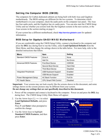
Transcription
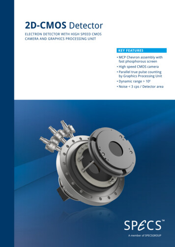
2D-CMOS DetectorELECTRON DETECTOR WITH HIGH SPEED CMOSCAMERA AND GRAPHICS PROCESSING UNITKEY FEATURES MCP Chevron assembly withfast phosphorous screen High speed CMOS camera Parallel true pulse countingby Graphics Processing Unit Dynamic range 106 Noise 3 cps / Detector areaA member of SPECSGROUP
INNOVATION IN SURFACE SPECTROSCOPYAND MICROSCOPY SYSTEMSSPECS leads the way in developingcutting-edge components and systems forgroundbreaking new surface analysis tools.SPECS Surface Nano Analysis GmbHAssembly of a systemcomponent for final testingSPECS engineer duringelectron detector mounting2D-CMOS DetectorSPECS Surface Nano Analysis GmbH headquarters is situated in the center of Germany’s capital Berlin with subsidiaries in Switzerland, USAand China. SPECS has attracted a talented teamof scientists and engineers who have dedicatedtheir knowledge and experience to the development, design, and production of instruments forsurface science, materials research, and nanotechnology for almost 30 years.In order to continuously improve performanceand to make available latest developments, weare in contact with numerous scientists, usersand customers from all over the world. Reliable quality control (ISO 9001 certified) andexcellent fast service, both remote and onsite, ensures maximum uptime and long-termoperation and reliability of SPECS instrumentsover many years.
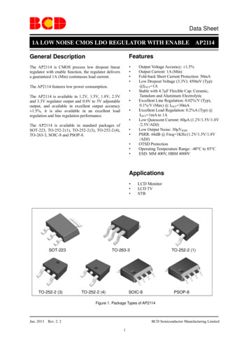
2D-CMOS DetectorNEXT GENERATION ELECTRON DETECTOR FOR ANGLERESOLVED PHOTOELECTRON SPECTROSCOPY (ARPES)Two dimensional MCP Detector withHigh Speed CMOS Camera and GraphicsProcessing Unit2D-CCD DetectorsTechnical ConceptAn MCP chevron assembly with a phosphor screenis used for electron detection. A single electronenters the MCP stack, being accelerated and multiplied. This packet of electrons (representing asingle electron or event) then impinges onto thephosphor coating on the screen causing fluorescence. A camera is recording the entire phosphorscreen image. In general MCP-phosphor stackDetection principle of MCP chevron stack with phosphor screendetectors have an unrivaled homogeneity, butalso an inherent non-linearity in the process ofdetection. A single electron becomes a cascade ofvarying number of electrons. Through this, thereis no one-to-one intensity correspondence withthe input electron, and instead the cascade hasa spread that is defined by MCP shape and voltage. This inherent non-linearity leads in part tothe resulting phosphor light to be non-linear inits response to electrons. This problem persistsinto the measured spectral intensity, as the intensity measured by the camera is the phosphorlight intensity. In addition to non-linearity, conventional detection schemes that measure thelight intensity of the phosphor in the detectionstack are susceptible to phosphor blooming. It ispossible that the phosphor itself has a non-linearand a spatially extended response which can negatively influence the data. The standard detector for ARPES nowadays works with CCD cameramounted to the detector, allowing for excellentlateral ( angle and energy) resolutions. It can beoperated in an analog mode in which the integrated light intensity is used for counting, or in pulsecounting mode in which individual light blobs aredetected. Both modes as used in standard CCDdetectors have disadvantages. In pulse countingmode conventional CCD detectors show saturation at high count rates. In analog mode the detection is non-linear at low count rates.Detector linearity of different counting modes
The new 2D-CMOS DetectorDetection PrincipleCMOS CameraTo overcome these limitations SPECS presents anew generation of 2D imaging detectors for highest resolution electron spectroscopy. The newdetector features a superior dynamic range andan extremely low noise level. The detection concept was developed in the group of Dan Dessau(University of Colorado). It is a true pulse counting algorithm converting the analog light signalto discriminated events. In order to be useful,this pulse counting algorithm must be able tokeep up with the rate of events in usual experiments. To do this, the traditional CCD camerais replaced with a high-speed CMOS camera. Tokeep up with the high data volume the data isprocessed in a highly parallel environment on aGraphics Processing Unit (GPU).The latest improvements in semiconductor technology have greatly increased the capabilities ofCMOS sensor. The used camera system featuresa Sony‘s IMX174 CMOS sensor. The fast 1/1.2“CMOS offers a resolution of 1920x1200 pixelsand frame rates up to 160 fps. This sensor offersthe extreme sensitivity required for the lowestlight situations while providing superior signalto-noise ratio, resolution, field-of-view, andframe rates.Detection principle: the multiple CPU cores of the GPUprocess sub-images as sections of the whole image inparallel2D-CMOS DetectorDynamic Range and MaximumCount RateThe dynamic range of the new imaging detectorhas been determined by XPS electron spectroscopy. The measured count rate has been plotted against the sample current. For this, the detector was mounted to a PHOIBOS 225 analyzer.The dynamic range is given by the minimum andmaximum measured count rate being in the linear regime. It is shown in the figures on the rightside that the new high speed imaging detector islinear at least in a dynamic range of 106 and it candetect events linearly from 4 cps to 4 Mcps.
5PerformanceARPES DataBismuth strontium calcium copper oxide (BSCCO), also known as cuprates, is a family of hightemperature superconductors having the generalized chemical formula Bi2Sr2Can-1CunO2n 4 x ,withn 2 being the most commonly studied compound (Bi-2212). The data were measured usinga PHOIBOS 225 analyzer equipped with the newhigh speed 2D-CMOS imaging detector.Dynamic range and maximum count rate of a 2D-CMOSdetectorNoise LevelNo background subtraction was done. The offset due to constant dark noise (originating fromspontaneous emission of counts from the MCPs)is visible in the data points for lowest count rates. The background count rate is about 2.8 cpsacross the detector (0.0015 cps/energy channel).Laser-ARPES on the superconducting gap of off-nodalBi-2212 at 60K using 6eV photons is shown. Panel (a)shows the 2D ARPES spectrum where the x-axis hasbeen converted to momentum and the y-axis has beenconverted from kinetic energy to binding energy. Panel(b) shows an example MDC cut, in this case taken atE EF. Panel (c) shows an example EDC, in this case taken at k kF. The two line cuts are shown on the ARPESspectrum as light blue lines. Data courtesy S. P. Parhamand D. Dessau (University of Colorado, Boulder).
PHOIBOS SeriesULTIMATE PERFOMANCE ELECTRON ENERGY ANALYZERSPHOIBOS 100/150/225Design and ConceptThe latest design of the PHOIBOS hemisphericalenergy analyzer is currently in its 7th generation. Even though the design of the hemisphericalanalyzers has not significantly changed duringthe last 25 years of solid state physics, their performance still reaches outstanding values withmodern electronics and light sources. The longterm experience combined with modern electronics allows to study the materials propertieswith extremely high quality. SPECS permanentlycontinues to improve the PHOIBOS series without touching the well-established and provenstandards on the hemispherical analyzer type.The PHOIBOS analyzer is the standard stateof–the-art analyzer model for various analysismethods such as XPS/UPS and ARPES, as well asAES, ISS and microscopy solutions. It comes inthree sizes: 100mm mean radius, 150mm and225mm, with increasing transmission efficiencyand energy resolution. All analyzers are capable of all standard detectors and the 150/225 arein addition capable of being equipped with spindetectors. The awarded design of the analyzer isset up from a sophisticated lens system, providing real raw data with high transmission and astable hemispherical energy analyzer design. Thehardware is run by a highly stable and reliableelectronics. The standard configuration allowsthe detection of up to 3.5 kV. For high energy analysis, HV versions of the PHOIBOS 150 and 225analyzers are available.The new 2D-CMOS detector is also retrofittable toexisting PHOIBOS analyzers, not being limited tothe latest release. Thus the performance can significantly improve by just exchaning the detector.ElectronicsPHOIBOS 150 2D-CMOS2D-CMOS DetectorThe HSA electronics for the control of the SPECSanalyzer series is a reliable and versatile controlunit for photoelectron spectroscopy. The modular design of the power supply configurationcan be used for different applications such asstandard ARPES/XPS analyzers, but also for NAPanalyzers and Spin detectors. Customized configurations for special applications are availableon demand.
7To account for the various experiments the HSAcomes in three basic versions: the /- 3.5 kVversion and the high voltage 7 kV and 15 kVversions. Special HSA versions for Spin detectors are included in the detector packages. TheHSA is a bipolar power supply, allowing tocontrol photoelectron experiments as wellthe processing of ions inside the analyzer forISS spectroscopy.HSA 3500 ElecronicsTechnical DataSpecifications2D-CMOS DetectorCount rate linearityrange 6x10⁶ cpsNoise 3 cps full detector area 0.002 cps per energy channelDynamic Range 106Typical lateralresolution 60 µmChannels1920x1200Binning1,2,3,4,5,6,8 and 10Frame Rate160 fpsMulti Hit Capability 5000 (within 40 fs)MCP StackChevron, Imaging Quality, 2dend spoilingPhosphorusGd2O2S:Tb (P 43), decay time(90% to 10%) 1 msDimensions of 2D-CMOS Detector for PHOIBOS 150
c/o SPECS Surface Nano Analysis GmbHVoltastrasse 513355 Berlin / Germanywww.specs-group.comT 49 (0)30 46 78 24-0F 49 (0)30 46 42 083E imfo@specs.comVersion 02.05
Both modes as used in standard CCD detectors have disadvantages. In pulse counting mode conventional CCD detectors show saturati-on at high count rates. In analog mode the detec- tion is non-linear at low count rates. Detection principle: the multiple CPU cores of the GPU process sub-images as sections of the whole image in parallel-Detector The new 2D-CMOS Detector Detection Principle To .