Transcription
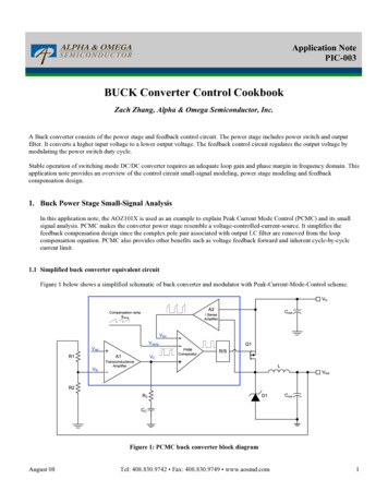
Application NotePIC-003BUCK Converter Control CookbookZach Zhang, Alpha & Omega Semiconductor, Inc.A Buck converter consists of the power stage and feedback control circuit. The power stage includes power switch and outputfilter. It converts a higher input voltage to a lower output voltage. The feedback control circuit regulates the output voltage bymodulating the power switch duty cycle.Stable operation of switching mode DC/DC converter requires an adequate loop gain and phase margin in frequency domain. Thisapplication note provides an overview of the control circuit small-signal modeling, power stage modeling and feedbackcompensation design.1. Buck Power Stage Small-Signal AnalysisIn this application note, the AOZ101X is used as an example to explain Peak Current Mode Control (PCMC) and its smallsignal analysis. PCMC makes the converter power stage resemble a voltage-controlled-current-source. It simplifies thefeedback compensation design since the complex pole pair associated with output LC filter are removed from the loopcompensation equation. PCMC also provides other benefits such as voltage feedback forward and inherent cycle-by-cyclecurrent limit.1.1 Simplified buck converter equivalent circuitFigure 1 below shows a simplified schematic of buck converter and modulator with Peak-Current-Mode-Control scheme.Figure 1: PCMC buck converter block diagramAugust 08Tel: 408.830.9742 Fax: 408.830.9749 www.aosmd.com1
Application NotePIC-003The output voltage is fed back to error amplifier A1 and is compared against the internal reference voltage, Vref, which is0.8V for the AOZ101x. Any slight difference between the feedback voltage and reference voltage results in large swing inthe error amplifier output voltage. The output voltage of error amplifier A1 is also called control voltage, which actuallycontrols the switch current level and the output voltage.The inductor ripple current is translated into a ramp voltage signal by the current sense amplifier A2, which amplifies thevoltage drop across the high side switch. This ramp represents the inductor current plus compensation ramp signal togetherand is fed back to the PWM comparator, forming an inner current control loop.At the beginning of each switching period, control voltage is higher than the current signal voltage. The output of the PWMcomparator is high and the high-side switch is on. The input voltage applies to the output filter inductor, L. The inductorcurrent increases at a constant slew rate decided by input voltage, output voltage, inductance and switching frequency. Theinductor current ramp up slew rate is:ΔIL is the peak to peak inductor current ripple. Δton is the high-side switch turn on time.The current signal voltage ramps up as the switch current increasing. When the current signal voltage, V Isn, equals to thecontrol voltage VC, the PWM comparator output changes from high to low. The high-side switch turns off and inductorcurrent starts to decay. The inductor current ramp down slew rate is:Δtoff is the high side switch turn off time.As explained above, control voltage signal, VC, is compared against current sense signal and determines the peak inductorcurrent level. Higher VC regulates peak inductor current to higher level. If VC is zero, inductor current is regulated to zero.If inductor is not saturated, there is a constant difference between average inductor current and peak inductor current.Where IL peak is the peak inductor current; IL average is the average inductor current, it is also the output current.The control voltage, VC, controls peak inductor current. If the inductor ripple current ΔIL is small, VC also controls averageinductor current. So the output filter inductor and PWM comparator together can be simplified to a Voltage-ControlledCurrent-Source. The simplified buck converter power stage circuit is shown in Figure 2 below.August 08Tel: 408.830.9742 Fax: 408.830.9749 www.aosmd.com2
Application NotePIC-003Figure 2: Equivalent circuit of buck converter with CMCThe current sense amplifier, A2, has a transconductance GCS, which is defined as:Assuming the inductance is large enough and ripple can be ignored, the inductor current is same as the load current. Sincethe control voltage regulates the inductor current level, the VIsn in equation above can be replaced by control voltage VC.Then control voltage can be calculated using inductor current, output voltage and current sense circuit transconductance inthe equation below.1.2 Power stage open loop transfer functionThe power stage open loop transfer function is defined as the transfer function from control voltage to output voltage.From Figure 2 above, VO can be calculated easily by multiplying output current and output impedance as below.CO is the output capacitor. RCO is the output capacitor ESR. RL is the load resistance.Combine the two equations above to get power stage open loop transfer function.August 08Tel: 408.830.9742 Fax: 408.830.9749 www.aosmd.com3
Application NotePIC-003since RL ESR,Now it can be found that power stage open loop transfer function has one pole and one zero.The pole is called dominant pole or load pole:The zero is called ESR zero:The power stage transfer function has DC gain:Figure 3 below shows the bode plot of power stage open loop transfer function. The dash line and solid line show the bodeplots when converter is under light load and heavy load respectively. As load increases, load resistance RL decreases. Theload pole moves from low frequency to high frequency. Also, the open loop transfer function DC gain is reduced as loadcurrent increases.Figure 3: Bode plot of buck converter power stage2. Compensation Circuit Small Signal Analysis and Feedback DesignAOZ101x buck regulator IC uses a high bandwidth transconductance amplifier as error amplifier A1. A transconductanceamplifier is actually a Voltage-Controlled-Current-Source. It converts any error voltage at its input pins to a current flowingout of its output pin. The amplifier factor, Gea, is called transconductance gain. It is defined as:August 08Tel: 408.830.9742 Fax: 408.830.9749 www.aosmd.com4
Application NotePIC-003A transconductance amplifier block diagram and equivalent circuit are shown in Figure 4 below.Figure 4: Transconductance amplifier and equivalent circuitIn Figure 4 above, Ramp represents the output impedance of transconductance amplifier. An ideal transconductance hasinfinite output impedance, Ramp. For the transconductance amplifier in AOZ101x series IC, the output impedance is above2.5MΩ. RC and CC represent the external compensation RC network components.From AC point of view, the non-inverting pin of amplifier is connected to a DC reference voltage, which is a virtual ACground. Figure 5 below shows the simplified compensation circuit, which is part of the buck converter block diagramshown in Figure 2.Figure 5: Compensation circuit diagramAugust 08Tel: 408.830.9742 Fax: 408.830.9749 www.aosmd.com5
Application NotePIC-003The transfer function of the compensation circuit in Figure 5 is derived below.Whereis the voltage feedback divider gain, andSince Ramp RC. The equation above can be simplified as ···········(2.1)From the equation above, it can be seen that the compensator circuit has one pole and one zero.The compensation pole is:Since the Ramp is fairly large, this is located at very low frequency range.The compensation zero is also called ESR zero:Another parameter of transconductance amplifier is transconductance amplifier voltage gain, Gvea. It is defined as thetransconductance amplifier output voltage over input voltage when amplifier output is open. It is easy to understand that:SoThe compensation pole can also be expressed by:fP2 is a very low frequency pole because Ramp is very large. The low frequency pole fP2 can be approximated by an integrator.The example below shows how close this approximation is. For example, Ramp 2.5MΩ, CC 1000pF, Figure 6 belowcompares the bode plot of transfer function ofand.As shown in Figure 6, the difference between the two transfer function only exists at very low frequency range.August 08Tel: 408.830.9742 Fax: 408.830.9749 www.aosmd.com6
Application NotePIC-003Figure 6: Bode plot of T1(s) and T2(s)The larger the Ramp is, the less is the difference between T1(s) and T2(s). Finally, the transfer function of the compensationcircuit in Figure 5 can be approximated to equation below.The bode plot of the transfer function above is shown in Figure 7 below.Figure 7: Bode plot of simplified compensation circuitAugust 08Tel: 408.830.9742 Fax: 408.830.9749 www.aosmd.com7
Application NotePIC-003The compensation circuit has one zero and one integrator. The zero is:At frequency fZ2 and above, the compensator transfer function gain is:3. Close Loop Transfer FunctionAOZ101x converter employs a very simple one integrator (or one pole) and one zero compensation network. The integratorhelps to increase close loop gain at low frequency range. The zero is placed where the power stage dominant pole is at heavyload. This zero gives a 90 degree phase boost around the close loop gains cross over frequency to ensure an adequate closeloop phase margin.So the total close loop transfer function is:At the frequency fP1 (or fZ2), the close loop gain is:If the desired close loop transfer function cross over frequency is fCC. Based on mathematics and basic bode plot principle,there is:User can determine the desired close loop cross over frequency, fCC, using the equation above. Most parameters in equationabove are fixed for a buck converter except the compensation resistor RC. To realize the desired close loop frequencyresponse, the compensation resistor, RC, can be calculated using equation below.In the RC compensation network, the compensation resistor RC determines the close loop cross over frequency whenconverter power stage is fixed. The compensation capacitor CC determines the compensation zero. To ensure enough phasemargin, the compensation zero should be placed at where the power stage dominate pole is under full load condition.August 08Tel: 408.830.9742 Fax: 408.830.9749 www.aosmd.com8
Application NotePIC-003Figure 8 below illustrates the bode plot of power stage open loop transfer function, compensation circuit and close looptransfer function. It can be seen that feedback design process is actually to shape the bode plot of close loop transferfunction to desired position.Figure 8. Close loop transfer function bode plotAugust 08Tel: 408.830.9742 Fax: 408.830.9749 www.aosmd.com9
Application NotePIC-003Appendix I: Bode PlotsIn the design of a converter control system, it is necessary to work with frequency-dependent transfer function and bode plot. Thebode plot is a method to display the complex value of circuit gain and phase. The gain magnitude in dB is plotted against logfrequency. Phase angle is also plotted against same log frequency. Bode plot provides good visibility into the gain/phasecharacteristics of power supply control loop. The bode plot of control loop elements are simplified to straight lines. Calculation ofbode plot is simplified to adding the gain and phase. The phase angle of the gain at any frequency depends on the rate change ofgain magnitude vs. frequency. For a system like power converters, the system stability depends on phase margin, or its close loopgain slope.The bode plots of some basic circuit elements used in this application note are reviewed below.1.IntegratorIntegrator,, has gain slope of -20dB/decade. Its unity gain frequency is f 1. The phase shift is -90 . A proportionalintegrator,, also has slope of 20db/decade. But its unity gain frequency is f a. Their bode plots are shown in Figure 1below.Figure 1: Bode plot of integrator2.Single poleSingle pole,, has flat gain slope at frequency lower than fP 1/a. At frequency higher than fP, its gain slope is-20dB/decade. Its unity gain frequency is fP. Phase shift at fP is -45 and -90 in total. A proportional single pole,,has higher unity gain frequency at k·fP. Their bode plot are shown in Figure 2 below.Figure 2: Bode plot of single poleAugust 08Tel: 408.830.9742 Fax: 408.830.9749 www.aosmd.com10
Application NotePIC-0033.Single zeroSingle zero,, has flat gain slope at frequency lower than fP 1/a. At frequency higher than fP, its gain slope is20dB/decade. Its unity gain frequency is fZ. Phase shift at fZ is 45 and 90 in total.Figure 3: Bode plot of single zeroCopyright 2008 Alpha & Omega Semiconductor, Inc.August 08Tel: 408.830.9742 Fax: 408.830.9749 www.aosmd.com11
A Buck converter consists of the power stage and feedback control circuit. The power stage includes power switch and output filter. It converts a higher input voltage to a lower output voltage. The feedback control circuit regulates the output voltage by . Where is the voltage feedback divider gain, and Since R amp R C. The equation above .