Transcription
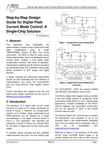
DIGITALStep-by-Step Design Guide for Digital Peak Current Mode Control: A Single-Chip SolutionRiStep-by-Step DesignGuide for Digital PeakCurrent Mode Control: ASingle-Chip . Ali Shirsavar1. tation of peak current mode control withslopecompensationusingansingleTMS320F28027 (Piccolo A) MCU from TexasInstruments. This MCU is ideal for peak currentmode implementation due to its dedicated internalcircuitry which enables a fully digital slopecompensation scheme. The theory of operation,mathematical modeling and all relevant equationsare presented along with a detailed step-by-stepdesign procedure in both analog and digitaldomains.A design example and associated experimentalresults are also presented with two methods ofimplementation; one using TI’s ControlSUITEand one using Biricha’s Chip Support Library(CSL).Further information with regards to the CSL anddigital power design workshops can be found atwww.biricha.com/workshops/2. IntroductionThe operation of a digital peak current modeconverter is similar to its analog counterpart asshown in Figure 1. However, the compensationnetwork, error amplifier, slope compensation andPWM generator are all replaced by a singlemicroprocessor in the digital converter shown inFigure 2. This application note describes theprocesses involved in setting up a Piccolo MCUfor use within a digital peak current mode powersupply.A complete design example and two completeimplementations are given; the first method usesDecember 2011VOROPWMBAN105Error AmpVREFRbFigure 1. Analog Peak Current Mode BuckConverterRiL0VSPWMC0BlankingComparatorC-by-C TripVOROPWMD 100%R1DAC- K2p2zController- ADCRbPiccolo ASlope CompensationREFFigure 2. Digital Peak Current Mode BuckConverterTI’s ControlSUITE whilst the second methoduses Biricha’s Chip Support Library (CSL).The Biricha Digital Chip Support Library providesa fast and simple method of configuring TexasInstruments C2000 MCUs for use in digital powerapplications. In-depth knowledge of the MCU’sinternal registers and associated configurationbits are not required; in place of this, simplefunction calls are used.The Biricha Digital CSL documentation containsfull descriptions and examples of all of thefunctions used in the implementation presentedhere. The user guides and an evaluation copy Referring to Figure 2, the operation of the peakcurrent mode controlled power supply is asfollows. Initially, the duty is set to 100% and thePage 1
DIGITALStep-by-Step Design Guide for Digital Peak Current Mode Control: A Single-Chip SolutionPWM is driven high. The output voltage of theconverter is applied to a sampling divider networkwhich is connected to the Piccolo’s ADC. Thevoltage is sampled and converted to a digitalvalue. A digital reference (REF) is subtracted fromthe digital value and the resulting error value isused as an input to the digital controller (2p2zController). This represents the error amplifier andcompensation network of the analog equivalent. Afull design procedure for this controller will begiven later on in this paper.The output of the controller is then multiplied by again term K. This gain scales the output of thecontroller to a digital value that is suitable for usewith the DAC of the comparator module,counteracting the effects of the various gainswithin the closed loop system. The value of thisgain term can be calculated to obtain the correctcrossover frequency; details are given in thedesign example.This scaled output is then used as an input to theDAC connected to the comparator’s invertinginput. The non-inverting input is connected to thecurrent sense transformer; the gain of this isrepresented by the Ri block. The current spikeassociated with turning the MOSFET switch on isignored through the use of leading edge blankingwithin the Piccolo’s blanking block. The output ofthe comparator will change state when theinductor current reaches the level of the voltageon the DAC output. This causes a cycle-by-cycletrip event to occur within the digital compare submodule of the PWM module. The PWM signal willbe low for the remainder of the switching period.Therefore, as with the analog equivalent, the dutyis determined by the peak of the inductor currentin the power stage of the converter. The digitalimplementation of peak current mode controlachieves the desirable cycle-by-cycle peakcurrent limiting effect of the analog equivalent.Full experimental results will be given shortly.AdvertisementDecember 2011BAN105Page 2
DIGITALStep-by-Step Design Guide for Digital Peak Current Mode Control: A Single-Chip Solution3. Peak Current Mode ModelThe Buck converter in Figure 3 is used todescribe the peak current mode model used inthis application note. However the sameprocedure can be applied to other topologies.L0VSPWMVOC0damped this resonant peak and reduces the gainat FS 2 .For a Buck converter, the required peak-to-peakvalue of the external compensation ramp hasbeen calculated in [2] and is given in Equation (2).This compensating ramp reduces the Q of thehigh frequency transfer function to 1.VPP RO(0.18 D )RiTSVINL0(2)Where:Figure 3. A typical Buck converterCurrent-sense transformer gain: RiIn order to design a stable compensator, we firstneed a mathematical model of the Buck converterplant. According to [3], this can be described bythree terms:Switching period: TSInput voltage: VIN1. FH (s ) , a high frequency transfer function.Output inductor: L02. H DC , a DC gain.The duty, D , is:3. H B (s ) , a power stage small signal model.D The complete control-to-output transfer functionfor a Buck converter under peak current modecontrol, as described in [1], is a combination ofthese three terms:VOV INWhere VO is the output voltage.With Q set to 1 FH (s ) simplifies to that given inEquation (3).V (s )H CO (s ) OUT FH (s ) H B (s ) H DCVERR (s )1FH (s ) (1)1 High Frequency Transfer FunctionsωN s2ω N2(3)The high frequency transfer function, FH (s ) , hasa double pole at half the switching frequency,FS 2 . Inevitably this will result in a resonant peakoccurring at this frequency. Therefore this peakneeds to be damped in order to avoid the gainBode plot crossing the 0dB axis at resonance andcausing instability.Where: 12 ωN π FS in rad / s i.e. Fs in Hz A compensating ramp is added to the system toeffectively damp resonant peak; this called “slopecompensation”. This is achieved by setting the Qof this double pole system to 1. A low Q forces aDecember 2011BAN105Page 3
DIGITALStep-by-Step Design Guide for Digital Peak Current Mode Control: A Single-Chip Solution- Pages Removed This is a preview version. To download the complete document please register on:www.biricha.com/registeror if you have already registered please login on:www.biricha.com/loginDecember 2011BAN105Page 4
DIGITALStep-by-Step Design Guide for Digital Peak Current Mode Control: A Single-Chip SolutionIMPORTANT NOTICEAll material presented in this application note, associated software, exercises, appendices and any oralpresentations made by or on behalf of Biricha Digital Power Ltd are for educational purposes only, are notintended for production or commercial applications and may contain irregularities and defects or errors.Furthermore, none of the material has been tested or certified by any government agency or industryregulatory organization or any other third party organization.Biricha Digital Power Ltd makes no warranties or representations, express, implied or statutory, includingany implied warranties of merchantability, fitness for a particular purpose, lack of viruses, lack of patentinfringements, accuracy or completeness of responses and lack of negligence. Prior to using, incorporatingor distributing any of the material that has been included in this application note in any commercial product,you must thoroughly test the product and the functionality in that product and be solely responsible for anyproblems or failures.In no event shall Biricha Digital Power Ltd, or any applicable licensor, be liable for any special, indirect,incidental, or punitive damages, however caused, arising in any way out of your use of the materialpresented in the DPS Workshop. These excluded damages include, but are not limited to, cost of removalor reinstallation, procurement of substitute goods or services, outside computer time, labour costs, loss ofdata, loss of goodwill, loss of profits, loss of savings, loss of use or interruption of business or othereconomic loss.Copyright Biricha Digital Power Ltd 2012December 2011BAN105Page 5
Step-by-Step Design Guide for Digital Peak Current Mode Control: A Single-Chip Solution 3. Peak Current Mode Model The Buck converter in Figure 3 is used to describe the peak current mode model used in this application note. However the same procedure can be applied to other topologies. L0 C0 RO PWM VS VO Figure 3. A typical Buck converter