Transcription
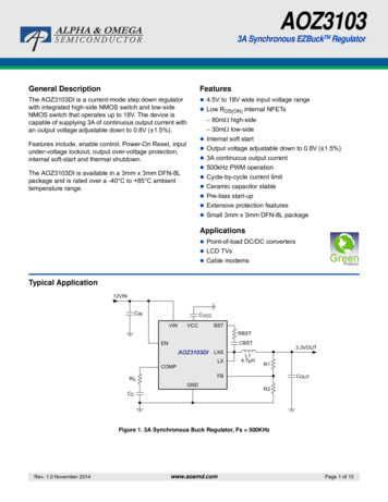
AOZ31033A Synchronous EZBuckTM RegulatorGeneral DescriptionFeaturesThe AOZ3103DI is a current-mode step down regulatorwith integrated high-side NMOS switch and low-sideNMOS switch that operates up to 18V. The device iscapable of supplying 3A of continuous output current withan output voltage adjustable down to 0.8V ( 1.5%). 4.5V to 18V wide input voltage range Low RDS(ON) internal NFETs– 80m high-side– 30m low-side Internal soft startFeatures include, enable control, Power-On Reset, inputunder-voltage lockout, output over-voltage protection,internal soft-start and thermal shutdown. Output voltage adjustable down to 0.8V ( 1.5%) 3A continuous output current 500kHz PWM operationThe AOZ3103DI is available in a 3mm x 3mm DFN-8Lpackage and is rated over a -40 C to 85 C ambienttemperature range. Cycle-by-cycle current limit Ceramic capacitor stable Pre-bias start-up Extensive protection features Small 3mm x 3mm DFN-8L packageApplications Point-of-load DC/DC converters LCD TVs Cable modemsTypical ILXSLXCOMPL14.7μH3.3VOUTR1FBRCGNDCCCOUTR2Figure 1. 3A Synchronous Buck Regulator, Fs 500KHzRev. 1.0 November 2014www.aosmd.comPage 1 of 13
AOZ3103Ordering InformationPart NumberAmbient Temperature RangePackageEnvironmentalAOZ3103DI-40 C to 85 C8-Pin 3mm x 3mm DFNGreen ProductAOS Green Products use reduced levels of Halogens, and are also RoHS compliant.Please visit www.aosmd.com/media/AOSGreenPolicy.pdf for additional information.Pin n 3mm x 3mm DFN(Top View)Pin DescriptionPin NumberPin Name1ENEnable Input. Logic high to enable the device.2LXSSource of the internal HS FET. This pin has to be externally connected to exposed padLX through the PCB.3VINSupply Input. When VIN rises above the UVLO threshold and EN is logic high, the devicestarts up.4GNDPower Ground.5BSTBootstrap. Requires a capacitor connection between LX and BST to form a floating supply across the high-side switch driver.6VCCInternal LDO Output.7COMP8Exposed PadRev. 1.0 November 2014Pin FunctionExternal Loop Compensation Pin. Connect a RC network between COMP and GND tocompensate the control loop.FBFeedback Input. The FB pin is used to set the output voltage with a resistive voltagedivider between the regulator’s output and AGND.LXSwitching Node. LX is the drain of the internal LS power FETs.www.aosmd.comPage 2 of 13
AOZ3103Absolute Maximum RatingsMaximum Operating RatingsExceeding the Absolute Maximum Ratings may damage thedevice.The device is not guaranteed to operate beyond theMaximum Operating ratings.ParameterRatingSupply Voltage (VIN)ENParameter20VSupply Voltage (VIN)20VOutput Voltage Range-0.7V to VIN 0.3VLX to GNDLX to GND (20ns)-5V to 22VVCC, FB, COMP to AGND-0.3V to 6VVBST to LX6VJunction Temperature (TJ) 150 CStorage Temperature (TS)-65 C to 150 CESD Rating(1)2kVRating4.5V to 18V0.8V to 0.85*VINAmbient Temperature (TA)-40 C to 85 CPackage Thermal Resistance(θJA)(2)50 C/WNote:2. The value of θJA is measured with the device mounted on a 1-in2FR-4 four layer board with 2oz copper and Vias, in a still air environment with TA 25 C. The value in any given application depends onthe user’s specification board design.Note:1. Devices are inherently ESD sensitive, handling precautions arerequired. Human body model rating: 1.5k in series with 100pF.Electrical CharacteristicsTA 25 C, VIN VEN 12V, VOUT 3.3V, unless otherwise specified(3).SymbolVINVCC UVLOVCCParameterConditionsSupply VoltageUnder-Voltage Lockout ThresholdVIN risingVIN fallingVCC RegulatorICC 5mASupply Current (Quiescent)IOUT 0V, VFB 1.2V,VEN 2VIOFFShutdown Supply CurrentVEN 0VVFBFeedback VoltageTA 25 CLoad Regulation0.1A IOUT 2.9ALine Regulation8V VIN 16VIFBFB Input CurrentVENEN Input ThresholdVEN HYSEN Input HysteresisTyp.4.5VCC Load RegulationIINMin.Off thresholdOn threshold0.788MaxUnits18V4.13.7V5V3%0.8mA25 A0.8000.812V0.5%1%200nA0.6V2250EN Leakage CurrentmV A10SS Time4msModulatorfOFrequency400500600kHzDMAXMaximum Duty Cycle85%TMINControllable Minimum On Time90nsCurrent Sense Transconductance8A/VError Amplifier Transconductance500 A/VRev. 1.0 November 2014www.aosmd.comPage 3 of 13
AOZ3103Electrical Characteristics (Continued)TA 25 C, VIN VEN 12V, VOUT 3.3V, unless otherwise .56.5UnitsProtectionILIMCurrent Limit3.5AOver Voltage ProtectionShutdown thresholdRecovery threshold950850Over Temperature Shutdown LimitTJ risingTJ falling150100 CHS RDS(ON)High-Side Switch On-ResistanceVBST-LX 5V80m LS RDS(ON)Low-Side Switch On-ResistanceVCC 5V30m VOVPmVOutput StageNote:3. The device is not guaranteed to operate beyond the Maximum Operating Ratings.Functional Block DiagramBSTVCCUVLO& PORENVIN5V LDORegulatorISENReferenceSoft Start& ifterLXS FETDriverLXQ2500KHzOscillatorCOMPGNDRev. 1.0 November 2014www.aosmd.comPage 4 of 13
AOZ3103Typical Performance CharacteristicsCircuit of Typical Application. TA 25 C, VIN VEN 12V, VOUT 3.3V, unless otherwise specified.Full Load OperationLight Load OperationLX5V/divLX10V/divIL1A/divVo ripple50mV/divVo ripple50mV/divVin ripple50mV/divVin ripple0.2V/divIL1A/div2μs/div2μs/divShort Circuit ProtectionShort Circuit 2A/div20ms/div20ms/divFull Load Start-up50% to 100% Load iv2ms/divRev. 1.0 November 2014100μs/divwww.aosmd.comPage 5 of 13
AOZ3103EfficiencyEfficiency vs. Load Current(VIN 12V, f 500kHz)100Efficiency (%)9080705VOUT, L 6.8μH3.3VOUT, L 4.7μH2.5VOUT, L 4.7μH1.8VOUT, L 2.2μH1.2VOUT, L 2.2μH60504000.51.01.52.02.53.0down by the external voltage divider at the FB pin. Thedifference of the FB pin voltage and reference isamplified by the internal transconductance erroramplifier. The error voltage, which shows on the COMPpin, is compared against the current signal, which is sumof inductor current signal and ramp compensation signal,at PWM comparator input. If the current signal is lessthan the error voltage, the internal high-side switch is on.The inductor current flows from the input through theinductor to the output. When the current signal exceedsthe error voltage, the high-side switch is off. The inductorcurrent is freewheeling through the internal low-side NMOSFET switch to output. The internal adaptive FETdriver guarantees no turn on overlap of both high-sideand low-side switch.Output Current (A)Detailed DescriptionThe AOZ3103DI is a current-mode step down regulatorwith integrated high-side NMOS switch and low-sideNMOS switch. It operates from a 4.5V to 18V inputvoltage range and supplies up to 3A of load current.Features include, enable control, Power-On Reset, inputunder voltage lockout, output over voltage protection,internal soft-start and thermal shut down.The AOZ3103DI is available in 8-pin 3mm x 3mm DFNpackage.Enable and Soft StartThe AOZ3103DI has internal soft start feature to limitin-rush current and ensure the output voltage ramps upsmoothly to regulation voltage. A soft start processbegins when the input voltage rises to 4.1V and voltageon EN pin is HIGH. In soft start process, the outputvoltage is typically ramped to regulation voltage in 4ms.The 4ms soft start time is set internally.The EN pin of the AOZ3103DI is active high. Connect theEN pin to VIN if enable function is not used. Pull it toground will disable the AOZ3103DI. Do not leave it open.The voltage on EN pin must be above 2V to enable thedevice. When the voltage on EN pin falls below 0.6V, theAOZ3103DI is disabled.Comparing with regulators using freewheeling Schottkydiodes, the AOZ3103DI uses freewheeling NMOSFET torealize synchronous rectification. It greatly improves theconverter efficiency and reduces power loss in the lowside switch.The AOZ3103DI uses a N-Channel MOSFET as thehigh-side switch. Since the NMOSFET requires a gatevoltage higher than the input voltage, a boost capacitor isneeded between LXS pin and BST pin to drive the gate.The boost capacitor is charged while LX is lowOutput Voltage ProgrammingOutput voltage can be set by feeding back the output tothe FB pin by using a resistor divider network. In theapplication circuit shown in Figure 1. The resistor dividernetwork includes R1 and R2. Usually, a design is startedby picking a fixed R2 value and calculating the requiredR1 with equation below.R 1 V O 0.8 1 ------- R 2 Some standard value of R1, R2 and most used outputvoltage values are listed in Table 1.VO (V)R1 (kΩ)R2 .5103.331.1105.052.310Steady-State OperationThe AOZ3103DI switching frequency is fixed and set byan internal oscillator. The practical switching frequencycould range from 400kHz to 600kHz due to devicevariation.The AOZ3103DI integrates an internal N-MOSFET asthe high-side switch. Inductor current is sensed byamplifying the voltage drop across the drain to source ofthe high side power MOSFET. Output voltage is dividedRev. 1.0 November 2014www.aosmd.comTable 1.Page 6 of 13
AOZ3103Combination of R1 and R2 should be large enough toavoid drawing excessive current from the output, whichwill cause power loss.Protection FeaturesThe AOZ3103DI has multiple protection features toprevent system circuit damage under abnormalconditions.Over Current Protection (OCP)The sensed inductor current signal is also used for overcurrent protection. Since the AOZ3103DI employs peakcurrent mode control, during over current conditions. Thepeak inductor current is automatically limited to cycle-bycycle, and if output is shorted to GND, then theAOZ3103DI will shutdown and auto restart approximatelyevery 25ms.circuit, the RMS value of input capacitor current can becalculated by:VO VO I CIN RMS I O --------- 1 – --------- V IN V IN if let m equal the conversion ratio:VO-------- mV INThe relation between the input capacitor RMS currentand voltage conversion ratio is calculated and shown inFigure 2 below. It can be seen that when VO is half of VIN,CIN it is under the worst current stress. The worst currentstress on CIN is 0.5 x IO.Power-On Reset (POR)0.5A power-on reset circuit monitors the VCC voltage. Whenthe input voltage exceeds 4.1V, the converter startsoperation. When input voltage falls below 3.7V, theconverter will be shut down.Thermal Protection0.4ICIN RMS(m) 0.3IO0.2An internal temperature sensor monitors the junctiontemperature. It shuts down the internal control circuit andhigh side NMOS if the junction temperature exceeds150 C. The regulator will restart automatically under thecontrol of soft-start circuit when the junction temperaturedecreases to 100 C.Application InformationThe basic AOZ3103DI application circuit is shown inFigure 1. Component selection is explained below.Input CapacitorThe input capacitor must be connected to the VIN pinand GND pin of the AOZ3103DI to maintain steady inputvoltage and filter out the pulsing input current. Thevoltage rating of input capacitor must be greater thanmaximum input voltage plus ripple voltage.The input ripple voltage can be approximated byequation below:000.5m1Figure 2. ICIN vs. Voltage Conversion RatioFor reliable operation and best performance, the inputcapacitors must have current rating higher than ICIN-RMSat worst operating conditions. Ceramic capacitors arepreferred for input capacitors because of their low ESRand high ripple current rating. Depending on theapplication circuits, other low ESR tantalum capacitor oraluminum electrolytic capacitor may also be used. Whenselecting ceramic capacitors, X5R or X7R type dielectricceramic capacitors are preferred for their bettertemperature and voltage characteristics. Note that theripple current rating from capacitor manufactures isbased on certain amount of life time. Further de-ratingmay be necessary for practical design requirement.InductorVO VOIO V IN ----------------- 1 – --------- --------V IN V INf C IN Since the input current is discontinuous in a buckconverter, the current stress on the input capacitor isanother concern when selecting the capacitor. For a buckRev. 1.0 November 20140.1The inductor is used to supply constant current to outputwhen it is driven by a switching voltage. For given inputand output voltage, inductance and switching frequencytogether decide the inductor ripple current, which is:VO VO I L ----------- 1 – --------- V IN f L www.aosmd.comPage 7 of 13
AOZ3103The peak inductor current is:1 V O I L ------------------------8 f C I LI Lpeak I O -------2OHigh inductance gives low inductor ripple current butrequires a larger size inductor to avoid saturation. Lowripple current reduces inductor core losses. It alsoreduces RMS current through inductor and switches,which results in less conduction loss. Usually, peak topeak ripple current on inductor is designed to be 20% to40% of output current.When selecting the inductor, make sure it is able tohandle the peak current without saturation even at thehighest operating temperature.The inductor takes the highest current in a buck circuit.The conduction loss on the inductor needs to be checkedfor thermal and efficiency requirements.Surface mount inductors in different shapes and stylesare available from Coilcraft, Elytone and Murata.Shielded inductors are small and radiate less EMI noise,but they do cost more than unshielded inductors. Thechoice depends on EMI requirement, price and size.Output CapacitorThe output capacitor is selected based on the DC outputvoltage rating, output ripple voltage specification andripple current rating.The selected output capacitor must have a higher ratedvoltage specification than the maximum desired outputvoltage including ripple. De-rating needs to beconsidered for long term reliability.Output ripple voltage specification is another importantfactor for selecting the output capacitor. In a buck converter circuit, output ripple voltage is determined byinductor value, switching frequency, output capacitorvalue and ESR. It can be calculated by the equationbelow:1 V O I L ESR CO ------------------------- 8 f C V O I L ESR COFor lower output ripple voltage across the entireoperating temperature range, X5R or X7R dielectric typeof ceramic, or other low ESR tantalum are recommendedto be used as output capacitors.In a buck converter, output capacitor current iscontinuous. The RMS current of output capacitor isdecided by the peak to peak inductor ripple current.It can be calculated by: I LI CO RMS ---------12Usually, the ripple current rating of the output capacitor isa smaller issue because of the low current stress. Whenthe buck inductor is selected to be very small andinductor ripple current is high, the output capacitor couldbe overstressed.Loop CompensationThe AOZ3103DI employs peak current mode control foreasy use and fast transient response. Peak current modecontrol eliminates the double pole effect of the outputL&C filter. It greatly simplifies the compensation loopdesign.With peak current mode control, the buck power stagecan be simplified to be a one-pole and one-zero systemin frequency domain. The pole is dominant pole can becalculated by:1f p1 ----------------------------------2 C O R LThe zero is a ESR zero due to output capacitor and itsESR. It is can be calculated by:Owhere,CO is output capacitor value andESRCO is the Equivalent Series Resistor of output capacitor.When a low ESR ceramic capacitor is used as outputcapacitor, the impedance of the capacitor at theswitching frequency dominates. Output ripple is mainlycaused by capacitor value and inductor ripple current.The output ripple voltage calculation can be simplified to:Rev. 1.0 November 2014If the impedance of ESR at switching frequencydominates, the output ripple voltage is mainly decided bycapacitor ESR and inductor ripple current. The outputripple voltage calculation can be further simplified to:1f z1 -----------------------------------------------2 C O ESR COwhere,CO is output filter capacitor,RL is load resistor value andESRCO is the Equivalent Series Resistor of output capacitor.The compensation design is actually to shape theconverter control loop transfer function to get desiredwww.aosmd.comPage 8 of 13
AOZ3103gain and phase. Several different types of compensationnetwork can be used for the AOZ3103DI. For mostcases, a series capacitor and resistor network connectedto the COMP pin sets the pole-zero and is adequate for astable high-bandwidth control loop.In the AOZ3103DI, FB pin and COMP pin are theinverting input and the output of internal error amplifier.A series R and C compensation network connected toCOMP provides one pole and one zero. The pole is:G EAf p2 ------------------------------------------2 C C G VEAThe compensation capacitor CC and resistor RC togethermake a zero. This zero is put somewhere close to thedominate pole fp1 but lower than 1/5 of selectedcrossover frequency. C2 can is selected by:1C C ----------------------------------2 R C f p1Equation above can also be simplified to:CO RLC C --------------------RCAn easy-to-use application software which helps todesign and simulate the compensation loop can be foundat www.aosmd.com.where,GEA is the error amplifier transconductance,which is 500 10-6 A/V;GVEA is the error amplifier voltage gain,which is 7000 V/V;Thermal Management and LayoutConsiderationCC is compensation capacitor in Figure 1.In the AOZ3103DI buck regulator circuit, high pulsingcurrent flows through two circuit loops. The first loopstarts from the input capacitors, to the VIN pin, to the LXpins, to the filter inductor, to the output capacitor andload, and then returns to the input capacitor throughground. Current flows in the first loop when the high sideswitch is on. The second loop starts from the inductor, tothe output capacitors and load, to the low side switch.Current flows in the second loop when the low sideswitch is on.The zero given by the external compensation network,capacitor C2 and resistor R3, is located at:1f z2 ----------------------------------2 C C R CTo design the compensation circuit, a target crossoverfrequency fC for close loop must be selected. The systemcrossover frequency is where control loop has unity gain.The crossover is the also called the converter bandwidth.Generally a higher bandwidth means faster response toload transient. However, the bandwidth should not be toohigh because of system stability concern. Whendesigning the compensation loop, converter stabilityunder all line and load condition must be considered.Usually, it is recommended to set the bandwidth to beequal or less than 1/10 of switching frequency.The strategy for choosing RC and CC is to set the crossover frequency with Rc and set the compensator zerowith CC. Using selected crossover frequency, fC, tocalculate R3:2 C OVOR C f C ---------- -----------------------------VG GFBEAfC is desired crossover frequency. For best performance, fC isset to be about 1/10 of switching frequency;GCS is the current sense circuit transconductance,which is 8 A/V.Rev. 1.0 November 2014P total loss V IN I IN – V O I OP inductor loss IO2 R inductor 1.1where,GEA is the error amplifier transconductance,which is 500 10-6 A/V;In the AOZ3103DI buck regulator circuit, the major powerdissipating components are the AOZ3103DI and outputinductor. The total power dissipation of the convertercircuit can be measured by input power minus outputpower.The power dissipation of inductor can be approximatelycalculated by output current and DCR of inductor.CSVFB is 0.8V;In PCB layout, minimizing the two loops area reduces thenoise of this circuit and improves efficiency. A groundplane is strongly recommended to connect the inputcapacitor, output capacitor and GND pin of theAOZ3103DI.The actual junction temperature can be calculated withpower dissipation in the AOZ3103DI and thermalimpedance from junction to ambient.T junction P total loss – P inductor loss JAwww.aosmd.comPage 9 of 13
AOZ3103The maximum junction temperature of AOZ3103DI is150ºC, which limits the maximum load current capability.The thermal performance of the AOZ3103DI is stronglyaffected by the PCB layout. Extra care should be takenby users during design process to ensure that the IC willoperate under the recommended environmentalconditions.Layout ConsiderationsSeveral layout tips are listed below for the best electricand thermal performance.1. The exposed pad (LX), which is the low-side NFETdrain, has to be externally connected to internal highside NFET source (LXS). Place a large copper planeto LX pin to help thermal dissipation.2. Do not use thermal relief connection to VIN and theGND pin. Pour a maximized copper area to the GNDpin and the VIN pin to help thermal dissipation.3. Input capacitor should be connected to the VIN pinand the GND pin as close as possible.Make the current trace from LX pins to L to CO to the GND asshort as possible.4. Pour copper plane on all unused board area andconnect it to stable DC nodes, like VIN, GND orVOUT.5. Keep sensitive signal traces such as feedback tracefar away from the LX pins.Rev. 1.0 November 2014www.aosmd.comPage 10 of 13
AOZ3103Package Dimensions, DFN 3x3B, 8 Lead EP1 PDD1bA1L1θ1E E1E2KLceABOTTOM VIEWSIDE VIEWTOP VIEWRECOMMENDED LAND PATTERN0.400.652.70001.251.40Dimensions in inchesDimensions in 051.100.600.5750.3000 0 .1012 50.1140.1200.0430.0240.0230.01200 50.016--10 0.0270.0200.00412 0.3250UNIT: MMNotes:1. Package body sizes exclude mold flash and gate burrs. Mold flash at the non-lead sides should be less than 6mils each.2. Controlling dimensions are in millimeters. Converted inch dimensions are not necessarily exact.Rev. 1.0 November 2014www.aosmd.comPage 11 of 13
AOZ3103Tape and Reel Dimensions, DFN 3x3, EPCarrier TapeD0P1D1A-AE1K0E2EB0TP0P2A0Feeding DirectionUNIT: mmPackageA0B0K0D0DFN 3x3 EP3.40 0.103.35 0.101.10 0.101.50 0.10/-0D11.50 0.10/-0E12.00 0.30E1E2P0P1P2T1.75 0.105.50 0.058.00 0.104.00 0.102.00 0.050.30 0.05ReelW1NSGKMVRHWUNIT: mmTape Size Reel Size12mmø330Mø330.0 0.50Nø97.0 1.0W13.0 0.30W117.4 1.0Hø13.0 0.5/-0.2K10.6S2.0 0.5G—R—V—Leader/Trailer and OrientationUnit Per Reel:5000pcsTrailer Tape300mm min.Rev. 1.0 November 2014Components TapeOrientation in Pocketwww.aosmd.comLeader Tape500mm min.Page 12 of 13
AOZ3103Part MarkingAOZ3103DI(3x3 DFN-8)3 1 0 3Industrial Temperature RangeNo OptionI 0 A WL TPart Number CodeWeek (Year code is embeddedby using upper dot, on “W”)Assembly LocationAssembly Lot NumberLEGAL DISCLAIMERApplications or uses as critical components in life support devices or systems are not authorized. AOS doesnot assume any liability arising out of such applications or uses of its products. AOS reserves the right tomake changes to product specifications without notice. It is the responsibility of the customer to evaluate suitabilityof the product for their intended application. Customer shall comply with applicable legal requirements,including all applicable export control rules, regulations and limitations.AOS' products are provided subject to AOS' terms and conditions of sale which are set forth at:http://www.aosmd.com/terms and conditions of saleLIFE SUPPORT POLICYALPHA AND OMEGA SEMICONDUCTOR PRODUCTS ARE NOT AUTHORIZED FOR USE AS CRITICALCOMPONENTS IN LIFE SUPPORT DEVICES OR SYSTEMS.As used herein:1. Life support devices or systems are devices orsystems which, (a) are intended for surgical implant intothe body or (b) support or sustain life, and (c) whosefailure to perform when properly used in accordancewith instructions for use provided in the labeling, can bereasonably expected to result in a significant injury ofthe user.Rev. 1.0 November 20142. A critical component in any component of a lifesupport, device, or system whose failure to perform canbe reasonably expected to cause the failure of the lifesupport device or system, or to affect its safety oreffectiveness.www.aosmd.comPage 13 of 13
AOZ3103 Rev. 1.0 November 2014 www.aosmd.com Page 4 of 13 Protection ILIM Current Limit 3.5 4.5 6.5 A VOVP Over Voltage Protection Shutdown threshold Recovery threshold 950 850 mV Over Temperature Shutdown Limit TJ rising TJ falling 150 100 C Output Stage HS RDS(ON) High-Side Switch On-Resistance VBST-LX 5V 80 m LS RDS(ON) Low-Side Switch On-Resistance VCC 5V 30 m