Transcription
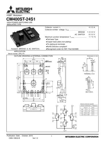
IGBT Modules CM400ST-24S1HIGH POWER SWITCHING USEINSULATED TYPEfourpack (BRIDGE & AC SWITCH)Collector current IC . . 4 0Collector-emitter voltage VCES . BRIDGE 1 2 0AC SWITCH6 5Maximum junction temperature T v j m a x . 1 7 Flat base Type Copper base plate (non-plating) Tin plating pin terminals RoHS Directive compliant* Recognized under UL1557, File E3235850A0V0V5 CAPPLICATION3level inverter, UPS, PVOUTLINE DRAWING & INTERNAL CONNECTIONDimension in mmTERMINAL t 0.8SECTION ATolerance otherwise specifiedPCDivision of Es1Cs4Di3G3Tr3NTCCs3ACPublication Date : October 2015CMH-10632-BVer.1.21TH1TH2to3Tolerance 0.2over3to6 0.3over6to30 0.5over 30to 120 0.8over 120to 400 1.2
IGBT Modules CM400ST-24S1HIGH POWER SWITCHING USEINSULATED TYPEMAXIMUM RATINGS (Tvj 25 C, unless otherwise specified)BRIDGE PART IGBT/DIODE (Tr1, Tr4, Di1, Di4)RatingUnitVCESSymbolCollector-emitter voltageG-E short-circuited1200VVGESGate-emitter voltageC-E short-circuited 20VICItemPtotIEIERM(Note1)400Pulse, Repetitive, VGE 15 VTotal power dissipation(Note1)(Note2, 4)DC, TC 103 CCollector currentICRMConditionsTC 25 CDCEmitter current(Note3)A800(Note2, 4)2340(Note2)W400Pulse, Repetitive(Note3)A800AC SWITCH PART IGBT/DIODE (Tr2, Tr3, Di2, Di3)RatingUnitVCESSymbolCollector-emitter voltageG-E short-circuited650VVGESGate-emitter voltageC-E short-circuited 20VICItemDC, TC 95 CCollector currentICRMPtotIEIERM(Note1)(Note2, 4)400Pulse, Repetitive, VGE 15 VTotal power dissipation(Note1)ConditionsTC 25 CDCEmitter current(Note3)A800(Note2, 4)1415(Note2)W400Pulse, olation voltageItemTerminals to base plate, RMS, f 60 Hz, AC 1 minConditions4000VTvjmaxMaximum junction temperatureInstantaneous event (overload)175TCmaxMaximum case temperature(Note4)125TvjopOperating junction temperatureContinuous operation (under switching)-40 150TstgStorage temperature--40 125 C CELECTRICAL CHARACTERISTICS (T v j 25 C, unless otherwise specified)BRIDGE PART IGBT/DIODE (Tr1, Tr4, Di1, Collector-emitter cut-off currentVCE VCES, G-E short-circuited--1.0mAIGESGate-emitter leakage currentVGE VGES, C-E short-circuited--0.5μAVGE(th)Gate-emitter threshold voltageIC 40mA, VCE 10 V5.46.06.6VT v j 25 C-1.802.25Auxiliary TerminalT v j 125 C-2.00-(Note5)T v j 150 C-2.05-IC 400 A, VGE 15 V,VCEsat(Terminal)Collector-emitter saturation voltageVCEsat(Chip)CiesOutput capacitanceCresReverse transfer capacitanceQGGate chargetd(on)Turn-on delay timetrRise timetd(off)Turn-off delay timetfFall time-1.702.15T v j 125 C-1.90-(Note5)T v j 150 C-1.95---40VCE 10 V, G-E short-circuitedVCC(P-C) VCC(C-N) 300 V, IC 400A, VGE 15 VVCC(P-C) VCC(C-N) 300 V, IC 400 A, VGE 15 V,RG 1.6 Ω, Inductive load(Note1)Emitter-collector voltage(Note1)(Chip)Publication Date : October 600--150T v j 25 C-2.603.40Auxiliary TerminalT v j 125 C-2.16-(Note5)T v j 150 C-2.10-IE 400 A, G-E short-circuited,(Terminal)VECT v j 25 CChipInput capacitanceCoesVECIC 400 A, VGE 15 V,IE 400 A, G-E short-circuited,T v j 25 C-2.503.30ChipT v j 125 C-2.06-(Note5)T v j 150 C-2.00-2VVnFnCnsVV
IGBT Modules CM400ST-24S1HIGH POWER SWITCHING USEINSULATED TYPEELECTRICAL CHARACTERISTICS (Cont; T v j 25 C, unless otherwise specified)BRIDGE PART IGBT/DIODE (Tr1, Tr4, Di1, itVCC(P-C) VCC(C-N) 300 V, IE 400 A, VGE 15 V,--250nsReverse recovery chargeRG 0 Ω(Tr2/Tr3), Inductive load-16-μCTurn-on switching energy per pulseVCC(P-C) VCC(C-N) 300 V, IC IE 400 A,EoffTurn-off switching energy per pulseVGE 15 V, T v j 150 C,(Note1)LimitsTyp.Reverse recovery timeEonErrMin.RG(Tr1,4) 1.6 ΩRG(Tr2,3) 0 Ω-17.0--23.5-mJReverse recovery energy per pulseInductive load-7.0-mJR CC' EE'Internal lead resistanceMain terminals-chip, per switch,TC 25 C (Note4)--0.25mΩrgInternal gate resistancePer switch-4.9-ΩRECOMMENDED OPERATING CONDITIONSSymbolVCC(P-C)VCC(C-N)VGEonRGItem(DC) Supply voltageLimitsConditionsApplied across each of P to C and C to NGate (-emitter drive) voltageApplied across emitter to gate of each IGBTExternal gate resistancePer switchTr1, n.LimitsTyp.Max.--1.0mAVAC SWITCH PART IGBT/DIODE (Tr2, Tr3, Di2, Di3)SymbolItemConditionsICESCollector-emitter cut-off currentIGESGate-emitter leakage currentVGE VGES, C-E short-circuitedVGE(th)Gate-emitter threshold voltageIC 40mA, VCE 10 V(Terminal)Collector-emitter saturation voltageVCEsat(Chip)CiesInput capacitanceCoesOutput capacitanceCresReverse transfer capacitanceQGGate chargetd(on)Turn-on delay timetrRise timetd(off)Turn-off delay timetfFall time(Note1)(Terminal)Emitter-collector A5.46.06.6VT v j 25 C-1.351.75Auxiliary TerminalT v j 125 C-1.43-(Note5)T v j 150 C-1.45-IC 400 A, VGE 15 V,VCEsatVECVCE VCES, G-E short-circuitedIC 400 A, VGE 15 V,T v j 25 C-1.251.65ChipT v j 125 C-1.33-(Note5)T v j 150 C-1.35-VCE 10 V, G-E short-circuitedVCC(P-C) VCC(C-N) 300 V, IC 400 A, VGE 15 VVCC(P-C) VCC(C-N) 300 V, IC 400 A, VGE 15 V,RG 0 Ω, Inductive load-48-3.1--0.9-1450---350--150--500--300T v j 25 C-2.002.80Auxiliary TerminalT v j 125 C-1.95-(Note5)T v j 150 C-1.90-IE 400A, G-E short-circuited,T v j 25 C-1.902.70ChipT v j 125 C-1.85-(Note5)T v j 150 CVVnFnCnsVV-1.80-Reverse recovery timeVCC(P-C) VCC(C-N) 300 V, IE 400 A, VGE 15 V,--200nsReverse recovery chargeRG 1.6 Ω(Tr1/Tr4), Inductive load-16-μCTurn-on switching energy per pulseVCC(P-C) VCC(C-N) 300 V, IC IE 400 A,EoffTurn-off switching energy per pulseVGE 15 V, T v j 150 C,Err-IE 400 A, G-E short-circuited,Eon(Note1)UnitRG(Tr2,3) 0 Ω0.2-21.2-mJReverse recovery energy per pulseInductive load-15.3-mJR CC' EE'Internal lead resistanceMain terminals-chip, per switch,TC 25 C (Note4)--0.25mΩrgInternal gate resistancePer switch-1.5-ΩPublication Date : October 2015CMH-10632-BVer.1.2RG(Tr1,4) 1.6 Ω-3
IGBT Modules CM400ST-24S1HIGH POWER SWITCHING USEINSULATED TYPERECOMMENDED OPERATING CONDITIONSSymbolVCC(P-C)VCC(C-N)Item(DC) Supply voltageLimitsConditionsApplied across each of P to C and C to NVGEonGate (-emitter drive) voltageApplied across emitter to gate of each IGBTRGExternal gate resistancePer switchTr2, mitsTyp.Max.4.855.005.15kΩ-7.3- -0.106NTC THERMISTOR PARTSymbolItemConditions(Note4)R25Zero-power resistanceTC 25 C R/RDeviation of resistanceR100 493 Ω, TC 100 CB(25/50)B-constantApproximate by equationP25Power dissipationTC 25 C(Note4)(Note6)(Note4)UnitTHERMAL RESISTANCE QJunction to case, per BRIDGE PART IGBTRth(j-c)DJunction to case, per BRIDGE PART DIODE (Note4)Rth(j-c)QThermal resistanceJunction to case, per AC SWITCH PART IGBT(Note4)Rth(j-c)DJunction to case, per AC SWITCH PART DIODE (Note4)--0.165Rth(c-s)Case to heat sink, per 1 module,Thermal grease applied (Note4, 7)-0.011-Min.LimitsTyp.Max.Contact thermal resistanceUnitK/WK/WMECHANICAL CHARACTERISTICSSymbolItemConditionsUnitMtMounting torqueMain terminalsM 6 screw3.54.04.5N·mMsMounting torqueMounting to heat sinkM 5 screw2.53.03.5N·mmmass-gdsCreepage distancedaClearanceecFlatness of base plate-560-Terminal to terminal14.4--Terminal to base plate16.7--Terminal to terminal8.0--Terminal to base plate16.7---50- 100On the centerline X, Y(Note8)*: This product is This product is compliant with the Restriction of the Use of Certain Hazardous Substances in Electrical and Electronic Equipment(RoHS) directive 2011/65/EU.Note1.2.3.4.Represent ratings and characteristics of the anti-parallel, emitter-collector free wheeling diode (DIODE).Junction temperature (T v j ) should not increase beyond T v j m a x rating.Pulse width and repetition rate should be such that the device junction temperature (T v j ) dose not exceed T v j m a x rating.Case temperature (TC) and heat sink temperature (T s ) are defined on the each surface (mounting side) of base plate and heat sinkjust under the chips. Refer to the figure of chip location.5. Pulse width and repetition rate should be such as to cause negligible temperature rise.R 2511 ) /()6. B ( 25 / 50 ) ln(R 50T25 T50R25: resistance at absolute temperature T25 [K]; T25 25 [ C] 273.15 298.15 [K]R50: resistance at absolute temperature T50 [K]; T50 50 [ C] 273.15 323.15 [K]7. Typical value is measured by using thermally conductive grease of λ 0.9 W/(m·K).Publication Date : October 2015CMH-10632-BVer.1.24mmmmμm
IGBT Modules CM400ST-24S1HIGH POWER SWITCHING USEINSULATED TYPE-:Concave :Convex8. The base plate (mounting side) flatness measurement points (X, Y) are as follows of the next figure.YXmounting sidemounting sidemounting side-:Concave :Convex9. Use the following screws when mounting the printed circuit board (PCB) on the standoffs. "φ2.6 10 or φ2.6 12 B1 tapping screw"The length of the screw depends on thickness (t1.6 t2.0) of the PCB.CHIP LOCATION (Top view)Dimension in mm, tolerance: 1 mmTr1/Tr4: BRIDGE IGBT, Tr2/Tr3: AC SWITCH IGBT,Di1/Di4: BRIDGE DIODE, Di2/Di3: AC SWITCH DIODE,Th: NTC thermistor.rPublication Date : October 2015CMH-10632-BVer.1.25
IGBT Modules CM400ST-24S1HIGH POWER SWITCHING USEINSULATED TYPECvGEPG-VGETr1,Di1iEACTr3Di3CTr4,Di4Cs VGE0-VGEvCECsCvGEEEsGTr2Di20VVCC(P-N)CEEs GCs0iCC VGEGRG LoadEEs90 % Cs TEST CIRCUIT AND WAVEFORMS90 % -VGEiCNt10%0Atrtd(on)tftd(off )tSwitching test circuit and waveforms (BRIDGE PART s-VGECsGEEsNTr2Di2CGEs GRG VGE0-VGECs 0.5 I r rt r r , Q r r test waveformiEvCE0VCC(P-C)VCC(C-N)0.1 VCC(P-C)0.1 VCC(C-N)0.1 ICMICMVCC(P-C)VCC(C-N)t0tIrr-VGEiCiCtrr0ASwitching test circuit and waveforms (AC SWITCH PART switching)ICMQ r r 0.5 I r r t r rIEVCC(P-N)CEvCEiE LoadE0.1 VCC(P-C)0.1 VCC(C-N)titiIEMvECvCE0.02 ICMtVCC(P-C)VCC(C-N)0At0VttiIGBT Turn-on switching energyIGBT Turn-off switching energyDIODE Reverse recovery energyTurn-on / Turn-off switching energy and Reverse recovery energy test waveforms (Integral time instruction drawing)Publication Date : October 2015CMH-10632-BVer.1.26
IGBT Modules CM400ST-24S1HIGH POWER SWITCHING USEINSULATED TYPETEST CIRCUITCsVCPCsICGEsVGE 15V Tr1ETr3Di3CTr4Di4CCsGCsEsTr2Di2EEsVETr1Di1CEEs GCTr4Di4CsCsVNTr3Di3CsCCEs circuitedEsTr2Di2CCCsICETr1Di1EEs GVCsTr4Di4CsTr3Di3GVETr2Tr2Di2Es GEs GTr3Di3CTr4Di4CsCsVNCsCGTr2Di2CCEEs GCsShort-circuitedGEsIEENDi4PECsEsCTr4Di4CsVGE 15VCsCVGE 15VShort- EscircuitedTr3GETr2Di2CNACCEEs GCsCTr4Di4VCsCTr3Di3GVGShort- EscircuitedDi2PIEETr1Di1CsGNTr3Di3CGACCEV CE sa t characteristics test circuit (AC SWITCH PART)Publication Date : October 2015CMH-10632-BVer.1.2CTr1Di1CCsGShort- Tr2Di2VEC characteristics test circuit (BRIDGE PART)PCEVGE 15VNCsPDi1GACTr4Di4CTr4PEsTr3Di3CGACGV CE sa t characteristics test circuit (BRIDGE PART)CsECNTr1CsCEICEPIETr1Di1Short-circuitedGVGE Es Es GCCsVGE 15VNDi3VEC characteristics test circuit (AC SWITCH PART)7CE
IGBT Modules CM400ST-24S1HIGH POWER SWITCHING USEINSULATED TYPEPERFORMANCE CURVESBRIDGE PARTOUTPUTCHARACTERISTICS(TYPICAL)T v j 25 CCOLLECTOR-EMITTER SATURATION VOLTAGECHARACTERISTICS(TYPICAL)(Chip)VGE 15 V(Chip)3.580015 VVGE 20 V12 VT v j 150 C(V)3600COLLECTOR-EMITTERSATURATION VOLTAGE VCEsatCOLLECTOR CURRENT IC(A)70050011 V40030010 V2009V100T v j 125 C2.52T v j 25 C1.510.50002468COLLECTOR-EMITTER VOLTAGE010VCE100(V)COLLECTOR-EMITTER SATURATION A)FREE WHEELING DIODEFORWARD CHARACTERISTICS(TYPICAL)(Chip)G-E short-circuited10(Chip)1000VCEsat(V)T v j 25 C200COLLECTOR CURRENT ICIC 800 A(A)T v j 125 CIC 400 AEMITTER CURRENT IECOLLECTOR-EMITTER SATURATION VOLTAGE86IC 160 A4T v j 150 C100T v j 25 C201068101214GATE-EMITTER VOLTAGE16VGEPublication Date : October OLLECTOR VOLTAGE83VEC3.5(V)
IGBT Modules CM400ST-24S1HIGH POWER SWITCHING USEINSULATED TYPEPERFORMANCE CURVESBRIDGE PARTHALF-BRIDGESWITCHING CHARACTERISTICS(TYPICAL)HALF-BRIDGESWITCHING CHARACTERISTICS(TYPICAL)VCE 300 V, VGE 15 V, RG 1.6 Ω(Tr1/Tr4), INDUCTIVE LOAD---------------: T v j 150 C, - - - - -: T v j 125 CVCE 300 V, VGE 15 V, IC 400 A, INDUCTIVE LOAD---------------: T v j 150 C, - - - - -: T v j 125 C10001000td(off)td(on)tr10101000.11000COLLECTOR CURRENT IC(A)110EXTERNAL GATE RESISTANCEHALF-BRIDGESWITCHING CHARACTERISTICS(TYPICAL)VCE 300 V, VGE 15 V, RG 1.6 (Tr1/Tr4) Ω,INDUCTIVE LOAD, PER PULSE---------------: T v j 150 C, - - - - -: T v j 125 C100RG (Tr1/Tr4) (Ω)HALF-BRIDGESWITCHING CHARACTERISTICS(TYPICAL)VCE 300 V, VGE 15 V, IC 400 A,INDUCTIVE LOAD, PER PULSE---------------: T v j 150 C, - - - - -: T v j 125 C10010EoffEon10.10.01REVERSE RECOVERY ENERGY (mJ)100SWITCHING ENERGY (mJ)REVERSE RECOVERY ENERGY (mJ)tr, tf (ns)tf10010SWITCHING ENERGY (mJ)SWITCHING TIME100trSWITCHING TIMESWITCHING TIMEtrtd(on), tr, td(off) tf(ns)td(on), tr, td(off), tftd(on)SWITCHING OR CURRENT IC (A)EMITTER CURRENT IE (A)Publication Date : October 2015CMH-10632-BVer.1.21EXTERNAL GATE RESISTANCE910100RG (Tr1/Tr4) (Ω)
IGBT Modules CM400ST-24S1HIGH POWER SWITCHING USEINSULATED TYPEPERFORMANCE CURVESBRIDGE PARTHALF-BRIDGESWITCHING CHARACTERISTICS(TYPICAL)VCE 300 V, VGE 15 V, RG 0 Ω (Tr2/Tr3),INDUCTIVE LOAD, PER PULSE---------------: T v j 150 C, - - - - -: T v j 125 CHALF-BRIDGESWITCHING CHARACTERISTICS(TYPICAL)VCE 300 V, VGE 15 V, IE 400 A,INDUCTIVE LOAD, PER PULSE---------------: T v j 150 C, - - - - -: T v j 125 CErr10.10.011001000COLLECTOR CURRENT IE(A)1000Irr100trr1010100EMITTER CURRENT IEEMITTER CURRENT IEPublication Date : October 2015CMH-10632-BVer.1.21EXTERNAL GATE RESISTANCEVCE 300 V, VGE 15 V, RG 0 Ω (Tr2/Tr3), INDUCTIVE LOAD---------------: T v j 150 C, - - - - -: T v j 125 Ct r r (ns)Err0.1FREE WHEELING DIODEREVERSE RECOVERY CHARACTERISTICS(TYPICAL)(A)10110IrrSWITCHING TIMESWITCHING TIMEtr(ns)10tr, tf (ns)100REVERSE RECOVERY ENERGY (mJ)REVERSE RECOVERY ENERGY (mJ)1001000(A)(A)1010100RG (Tr2/Tr3) (Ω)
IGBT Modules CM400ST-24S1HIGH POWER SWITCHING USEINSULATED TYPEPERFORMANCE CURVESAC SWITCH R SATURATION VOLTAGECHARACTERISTICS(TYPICAL)T v j 25 C(Chip)VGE 15 V12 VVGE 20 V15 V3(V)11 V600COLLECTOR-EMITTERSATURATION VOLTAGE VCEsatCOLLECTOR CURRENT IC(A)70050010 V4003002009V2.5T v j 150 C2T v j 125 C1.5T v j 25 C10.51000002468COLLECTOR-EMITTER VOLTAGE010VCE100(V)T v j 25 C200300400500600COLLECTOR CURRENT ICCOLLECTOR-EMITTER SATURATION VOLTAGECHARACTERISTICS(TYPICAL)700800(A)FREE WHEELING DIODEFORWARD CHARACTERISTICS(TYPICAL)(Chip)G-E short-circuited(Chip)100010VCEsat(V)(Chip)3.5800IC 800 AT v j 150 C(A)IC 400 AEMITTER CURRENT IECOLLECTOR-EMITTER SATURATION VOLTAGE86IC 160 A4100T v j 125 C2T v j 25 C10068101214GATE-EMITTER VOLTAGE16VGEPublication Date : October OLLECTOR VOLTAGE113VEC3.5(V)
IGBT Modules CM400ST-24S1HIGH POWER SWITCHING USEINSULATED TYPEPERFORMANCE CURVESAC SWITCH PARTHALF-BRIDGESWITCHING CHARACTERISTICS(TYPICAL)HALF-BRIDGESWITCHING CHARACTERISTICS(TYPICAL)VCE 300 V, VGE 15 V, RG 0 Ω(Tr2/Tr3), INDUCTIVE LOAD---------------: T v j 150 C, - - - - -: T v j 125 CVCE 300 V, VGE 15 V, IC 400 A, INDUCTIVE LOAD---------------: T v j 150 C, - - - - -: T v j 125 C10001000tftd(on)td(off)tr, tf (ns)tfSWITCHING TIMESWITCHING TIME100td(on), tr, td(off), tfSWITCHING TIMEtd(on)tr100SWITCHING TIMEtrtd(on), tr, td(off) tf(ns)(ns)(ns)td(off)tr1010101001000COLLECTOR CURRENT IC0.1(A)110EXTERNAL GATE RESISTANCEHALF-BRIDGESWITCHING CHARACTERISTICS(TYPICAL)VCE 300 V, VGE 15 V, RG 0 (Tr2/Tr3) Ω,INDUCTIVE LOAD, PER PULSE---------------: T v j 150 C, - - - - -: T v j 125 C100RG (Tr2/Tr3) (Ω)HALF-BRIDGESWITCHING CHARACTERISTICS(TYPICAL)VCE 300 V, VGE 15 V, IC 400 A,INDUCTIVE LOAD, PER PULSE---------------: T v j 150 C, - - - - -: T v j 125 C100100Eoff10.1Eon0.01REVERSE RECOVERY ENERGY (mJ)10SWITCHING ENERGY (mJ)REVERSE RECOVERY ENERGY (mJ)SWITCHING ENERGY (mJ)EonEoff1010.11010010000.1COLLECTOR CURRENT IC (A)EMITTER CURRENT IE (A)Publication Date : October 2015CMH-10632-BVer.1.21EXTERNAL GATE RESISTANCE1210100RG (Tr2/Tr3) (Ω)
IGBT Modules CM400ST-24S1HIGH POWER SWITCHING USEINSULATED TYPEPERFORMANCE CURVESAC SWITCH PARTHALF-BRIDGESWITCHING CHARACTERISTICS(TYPICAL)VCE 300 V, VGE 15 V, RG 1.6 Ω (Tr1/Tr4),INDUCTIVE LOAD, PER PULSE---------------: T v j 150 C, - - - - -: T v j 125 CHALF-BRIDGESWITCHING CHARACTERISTICS(TYPICAL)VCE 300 V, VGE 15 V, IE 400 A,INDUCTIVE LOAD, PER PULSE---------------: T v j 150 C, - - - - -: T v j 125 CSWITCHING TIMEtrErr10.10.011001000COLLECTOR CURRENT IE1000Irrtrr1001010100EMITTER CURRENT IEEMITTER CURRENT IEPublication Date : October 2015CMH-10632-BVer.1.21EXTERNAL GATE RESISTANCEVCE 300 V, VGE 15 V, RG 1.6 Ω (Tr1/Tr4), INDUCTIVE LOAD---------------: T v j 150 C, - - - - -: T v j 125 Ct r r (ns)Err0.1(A)FREE WHEELING DIODEREVERSE RECOVERY CHARACTERISTICS(TYPICAL)(A)10110IrrSWITCHING TIME(ns)10tr, tf (ns)100REVERSE RECOVERY ENERGY (mJ)REVERSE RECOVERY ENERGY (mJ)1001000(A)(A)1310100RG (Tr1/Tr4) (Ω)
IGBT Modules CM400ST-24S1HIGH POWER SWITCHING USEINSULATED TYPEPERFORMANCE CURVESBRIDGE PARTCAPACITANCECHARACTERISTICS(TYPICAL)GATE CHARGECHARACTERISTICS(TYPICAL)G-E short-circuited, T v j 25 CVCC(P-N) 600 V, IC 400 A, Tvj 25 C10020(V)CiesGATE-EMITTER .1110COLLECTOR-EMITTER VOLTAGE100VCE0200(V)400600GATE CHARGE800QG10001200(nC)AC SWITCH PARTCAPACITANCECHARACTERISTICS(TYPICAL)GATE CHARGECHARACTERISTICS(TYPICAL)G-E short-circuited, T v j 25 CVCC(P-C) VCC(C-N) 300 V, IC 400 A, Tvj 25 C10020(V)CiesGATE-EMITTER .1110COLLECTOR-EMITTER VOLTAGEPublication Date : October 2015CMH-10632-BVer.1.2100VCE0(V)5001000GATE CHARGE141500QG(nC)2000
IGBT Modules CM400ST-24S1HIGH POWER SWITCHING USEINSULATED TYPEPERFORMANCE CURVESCOMMON PARTTRANSIENT THERMAL IMPEDANCECHARACTERISTICS(MAXIMUM)Single pulse, TC 25 CB R I D G E PA RT: R t h ( j - c ) Q 0.064 K/W, R t h ( j - c ) D 0.105 K/WA C S W I T C H PA RT: R t h ( j - c ) Q 0.106 K/W, R t h ( j - c ) D 0.165 K/WNORMALIZED TRANSIENT THERMAL 10.01TIME0.1110(S)NTC THERMISTOR ER(kΩ)10010.1-50-25025TEMPERATURE5075100125T ( C)Publication Date : October 2015CMH-10632-BVer.1.215
IGBT Modules CM400ST-24S1HIGH POWER SWITCHING USEINSULATED TYPEKeep safety first in your circuit designs!Mitsubishi Electric Corporation puts the maximum effort into making semiconductor products better and morereliable, but there is always the possibility that trouble may occur with them. Trouble with semiconductors may leadto personal injury, fire or property damage. Remember to give due consideration to safety when making your circuitdesigns, with appropriate measures such as (i) placement of substitutive, auxiliary circuits, (ii) use ofnon-flammable material or (iii) prevention against any malfunction or mishap.Notes regarding these materials These materials are intended as a reference to assist our customers in the selection of the Mitsubishisemiconductor product best suited to the customer's application; they do not convey any license under anyintellectual property rights, or any other rights, belonging to Mitsubishi Electric Corporation or a third party. Mitsubishi Electric Corporation assumes no responsibility for any damage, or infringement of any third-party'srights, originating in the use of any product data, diagrams, charts, programs, algorithms, or circuit applicationexamples contained in these materials. All information contained in these materials, including product data, diagrams, charts, programs and algorithmsrepresents information on products at the time of publication of these materials, and are subject to change byMitsubishi Electric Corporation without notice due to product improvements or other reasons. It is thereforerecommended that customers contact Mitsubishi Electric Corporation or an authorized Mitsubishi Semiconductorproduct distributor for the latest product information before purchasing a product listed herein.The information described here may contain technical inaccuracies or typographical errors. Mitsubishi ElectricCorporation assumes no responsibility for any damage, liability, or other loss rising from these inaccuracies orerrors.Please also pay attention to information published by Mitsubishi Electric Corporation by various means, includingthe Mitsubishi Semiconductor home page (www.MitsubishiElectric.com/semiconductors/). When using any or all of the information contained in these materials, including product data, diagrams, charts,programs, and algorithms, please be sure to evaluate all information as a total system before making a finaldecision on the applicability of the information and products. Mitsubishi Electric Corporation assumes noresponsibility for any damage, liability or other loss resulting from the information containedherein. Mitsubishi Electric Corporation semiconductors are not designed or manufactured for use in a device or systemthat is used under circumstances in which human life is potentially at stake. Please contact Mitsubishi ElectricCorporation or an authorized Mitsubishi Semiconductor product distributor when considering the use of a productcontained herein for any specific purposes, such as apparatus or systems for transportation, vehicular, medical,aerospace, nuclear, or undersea repeater use. The prior written approval of Mitsubishi Electric Corporation is necessary to reprint or reproduce in whole or in partthese materials. If these products or technologies are subject to the Japanese export control restrictions, they must be exportedunder a license from the Japanese government and cannot be imported into a country other than the approveddestination.Any diversion or reexport contrary to the export control laws and regulations of Japan and/or the country ofdestination is prohibited. Please contact Mitsubishi Electric Corporation or an authorized Mitsubishi Semiconductor product distributor forfurther details on these materials or the products contained therein. 2015 MITSUBISHI ELECTRIC CORPORATION. ALL RIGHTS RESERVED.Publication Date : October 2015CMH-10632-BVer.1.216
ICRM (Note3)Pulse, Repetitive, VGE 15 V 800 Ptot Total power dissipation TC 25 C (Note2, 4) 1415 W IE (Note1) (Note2 . Supply voltage Applied across each of P to C and C to N - 300 360 V VGEon Gate (-emitter drive) voltage Applied across emitter to gate of each IGBT 13.5 15.0 16.5 V RG External gate resistance Per switch .