Transcription
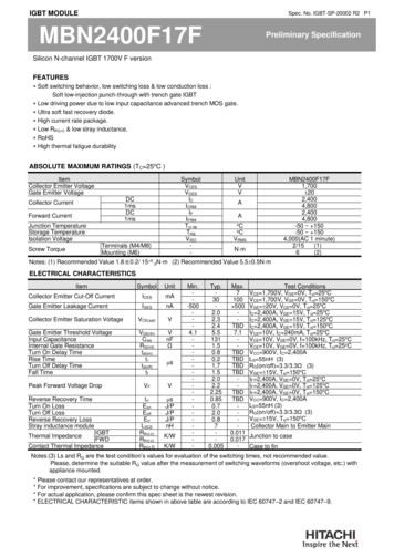
IGBT MODULESpec. No. IGBT-SP-20002 R2 P1MBN2400F17FPreliminary SpecificationSilicon N-channel IGBT 1700V F versionFEATURES Soft switching behavior, low switching loss & low conduction loss :Soft low-injection punch-through with trench gate IGBT Low driving power due to low input capacitance advanced trench MOS gate. Ultra soft fast recovery diode. High current rate package. Low Rth(j-c) & low stray inductance. RoHS High thermal fatigue durabilityABSOLUTE MAXIMUM RATINGS (TC 25oC )ItemCollector Emitter VoltageGate Emitter VoltageSymbolVCESVGESICICRMIFIFRMTvj opTstgVISO-DC1msDC1msCollector CurrentForward CurrentJunction TemperatureStorage TemperatureIsolation VoltageTerminals (M4/M8)Mounting (M6)Screw TorqueUnitVVMBN2400F17F1,700 202,4004,8002,4004,800-50 150-50 1504,000(AC 1 minute)2/15(1)6(2)AAoCoCVRMSN·mNotes: (1) Recommended Value 1.8 0.2/ 15 0-3N·m (2) Recommended Value 5.5 0.5N·mELECTRICAL CHARACTERISTICSItemSymbolUnitCollector Emitter Cut-Off CurrentICESmAGate Emitter Leakage CurrentIGESnACollector Emitter Saturation VoltageVCE(sat)VGate Emitter Threshold VoltageInput CapacitanceInternal Gate ResistanceTurn On Delay TimeRise TimeTurn Off Delay TimeFall EonEoffErrLSCERth(j-c)Rth(j-c)Rth(c-f) sJ/PJ/PJ/PnHPeak Forward Voltage DropReverse Recovery TimeTurn On LossTurn Off LossReverse Recovery LossStray inductance moduleIGBTFWDContact Thermal ImpedanceThermal Impedance .71.52.02.22.250.850.72.00.870.005Max.7100 500TBD7.1TBDTBDTBDTBDTBDTBD0.0110.017-Test ConditionsVCE 1,700V, VGE 0V, Tvj 25oCVCE 1,700V, VGE 0V, Tvj 150oCVGE 20V, VCE 0V, Tvj 25oCIC 2,400A, VGE 15V, Tvj 25oCIC 2,400A, VGE 15V, Tvj 125oCIC 2,400A, VGE 15V, Tvj 150oCVCE 10V, IC 240mA, Tvj 25oCVCE 10V, VGE 0V, f 100kHz, Tvj 25oCVCE 10V, VGE 0V, f 100kHz, Tvj 25oCVCC 900V, IC 2,400ALS 55nH (3)RG(on/off) 3.3/3.3Ω (3)VGE 15V, Tvj 150oCIF 2,400A, VGE 0V, Tvj 25oCIF 2,400A, VGE 0V, Tvj 125oCIF 2,400A, VGE 0V, Tvj 150oCVCC 900V, IC 2,400ALS 55nH (3)RG(on/off) 3.3/3.3Ω (3)VGE 15V, Tvj 150oCCollector Main to Emitter MainJunction to caseCase to finNotes:(3) Ls and RG are the test condition’s values for evaluation of the switching times, not recommended value.Please, determine the suitable RG value after the measurement of switching waveforms (overshoot voltage, etc.) withappliance mounted.* Please contact our representatives at order.* For improvement, specifications are subject to change without notice.* For actual application, please confirm this spec sheet is the newest revision.* ELECTRICAL CHARACTERISTIC items shown in above table are according to IEC 60747–2 and IEC 60747–9.
IGBT MODULESpec. No. IGBT-SP-20002 R2 P2MBN2400F17FPreliminary SpecificationOUTLINE DRAWINGUnit in mmLabelWeight : 1,300gCIRCUIT DIAGRAMCCCCEEEGE
IGBT MODULEMBN2400F17FSpec. No. IGBT-SP-20002 R2 P3Preliminary Specification
IGBT MODULEMBN2400F17FSpec. No. IGBT-SP-20002 R2 P4Preliminary Specification
IGBT MODULEMBN2400F17FSpec. No. IGBT-SP-20002 R2 P5Preliminary Specification
IGBT MODULEMBN2400F17FSpec. No. IGBT-SP-20002 R2 P6Preliminary Specification
IGBT MODULEMBN2400F17FSpec. No. IGBT-SP-20002 R2 P7Preliminary Specification
IGBT MODULESpec. No. IGBT-SP-20002 R2 P8MBN2400F17FPreliminary SpecificationHITACHI POWER SEMICONDUCTORSNotices1. Since mishandling of semiconductor devices may cause malfunctions, please be sure to read"Precautions for Safe Use and Notices" in the individual brochure before use.2. When designing an electronic circuit using semiconductor devices, please do not exceed theabsolute maximum rating specified for the device under any external fluctuations. And for pulseapplications, please also do not exceed the "Safe Operating Area (SOA)".3. Semiconductor devices may sometimes break down by accidental or unexpected surge voltage, soplease be careful about the safety design such as redundant design and malfunction preventiondesign which don't cause the damage expand even if they break down.4. In cases where extremely high reliability is required (such as use in nuclear power control,aerospace and aviation, traffic equipment, life-support-related medical equipment, fuel controlequipment and various kinds of safety equipment), safety should be ensured by using semiconductordevices that feature assured safety or by means of users’ fail-safe precautions or other arrangement.Or consult with Hitachi’s sales department staff. (When semiconductor devices fail, as a result thesemiconductor devices or wiring, wiring pattern may smoke, ignite, or the semiconductor devicesthemselves may burst.)5. A semi-processed article is done now using solder which contains lead inside the semiconductordevices. There is possibility of the regulation substance depend on the applied models, so pleasecheck before using.6. This specification is a material for component selection, which describes specifications of powersemiconductor devices (hereinafter referred to as products), characteristic charts, and externaldimension drawings.7. The information given herein, including the specifications and dimensions, is subject to changewithout prior notice to improve product characteristics. Before ordering, purchasers are advised tocontact with Hitachi power semiconductor sales department for the latest version of this data sheets.8. For handling other than described in this manual, follow the handling instructions (IGBT-HI-00002). For inquiries relating to the products, please contact nearest representatives that is located“Inquiry” portion on the top page of a home page.Hitachi power semiconductor home page vice.co.jp/en/
IGBT MODULEMBN2400F17FSpec. No. IGBT-SP-20002 R2 P9Preliminary SpecificationHITACHI POWER SEMICONDUCTORSUsage1. HPSD warrants that the HPSD products have the specified performance according to the respectivespecifications at the time of its sale. Testing and other quality control techniques of the HPSD productsby HPSD are utilized to the extent HPSD needs to meet the specifications described in this document.Not every device of the HPSD products is specifically tested on all parameters, except thosemandated by relevant laws and/or regulations.2. Following any claim regarding the failure of a product to meet the performance described in thisdocument made within one month of product delivery, all the products in relevant lot(s) shall be retested and re-delivered. The HPSD products delivered more than one month before such a claim shallnot be counted for such response.3. HPSD assumes no obligation nor makes any promise of compensation for any fault which should befound in a customer’s goods incorporating the products in the market. If a product failure occurs forreasons obviously attributable to HPSD and a claim is made within six months of product delivery,HPSD shall offer free replacement or payment of compensation. The maximum compensation shall bethe amount paid for the products, and HPSD shall not assume responsibility for any othercompensation.4. HPSD reserves the right to make changes in this document and to discontinue mass production of therelevant products without notice. Customers are advised to confirm specification of the product ofinquiry before purchasing of the products that the customer desired. Customers are further advised toconfirm before purchasing of such above products that the product of inquiry is the latest version andthat the relevant product is in mass production status if the purchasing of the products by the customeris suspended for one year or more.5. When you dispose of HPSD products and/or packing materials, comply with the laws and regulationsof each country and/or local government. Conduct careful preliminary studies about environmentallaws applying to your products such as RoHS, REACH. HPSD shall not assume responsibility forcompensation due to contravention of laws and/or regulations.6. HPSD shall not be held liable in any way for damages and infringement of patent rights, copyright orother intellectual property rights arising from or related to the use of the information, products, andcircuits in this document.7. No license is granted by this document of any patents, copyright or other intellectual property rights ofany third party or of HPSD.8. This document may not be reprinted, reproduced or duplicated, in any form, in whole or in part withoutthe express written permission of HPSD.9. You shall not use the HPSD products (technologies) described in this document and any otherproducts (technologies) manufactured or developed by using them (hereinafter called “END Products”)or supply the HPSD products (technologies) and END Products for the purpose of disturbinginternational peace and safety, including (ⅰ) the design, development, production, stockpiling or anyuse of weapons of mass destruction such as nuclear, chemical or biological weapons or missiles, (ⅱ)the other military activities, or (ⅲ) any use supporting these activities. You shall not sell, export,dispose of, license, rent, transfer, disclose or otherwise provide the HPSD products (technologies) andEND Products to any third party whether directly or indirectly with knowledge or reason to know thatthe third party or any other party will engage in the activities described above.10. When exporting, re-export transshipping or otherwise transferring the HPSD products (technologies)and END Products, all necessary procedures are to be taken in accordance with Foreign Exchangeand Foreign Trade Act (Foreign Exchange Act) of Japan, Export Administration Regulations (EAR) ofUS, and any other applicable export control laws and regulations promulgated and administered by thegovernments of the countries asserting jurisdictions over the parties or transaction.
Low driving power due to low input capacitance advanced trench MOS gate. . - 2.0 - I F 2,400A, V GE 0V, T vj 25oC - 2.2 - I F 2,400A, V GE 0V, T vj 125oC - 2.25 TBD I F 2,400A, V GE 0V, T vj . design which don't cause the damage expand even if they break down. 4. In cases where extremely high reliability is required (such as use in .