Transcription
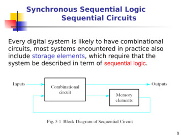
Synchronous Sequential LogicSequential CircuitsEvery digital system is likely to have combinationalcircuits, most systems encountered in practice alsoinclude storage elements, which require that thesystem be described in term of sequential logic.1
Synchronous ClockedSequential CircuitA sequential circuit may use many flip-flops to storeas many bits as necessary. The outputs can comeeither from the combinational circuit or from the flipflops or both.2
LatchesSR LatchThe SR latch is a circuit with two cross-coupled NORgates or two cross-coupled NAND gates. It has twoinputs labeled S for set and R for reset.3
SR Latch with NAND Gates4
SR Latch with Control InputThe operation of the basic SR latch can be modifiedby providing an additional control input thatdetermines when the state of the latch can bechanged. In Fig. 5-5, it consists of the basic SR latchand two additional NAND gates.5
D LatchOne way to eliminate the undesirable condition ofthe indeterminate state in SR latch is to ensure thatinputs S and R are never equal to 1 at the same timein Fig 5-5. This is done in the D latch.6
Graphic Symbols for latchesA latch is designated by a rectangular block withinputs on the left and outputs on the right. Oneoutput designates the normal output, and the otherdesignates the complement output.7
Flip-FlopsThe state of a latch or flip-flop is switched by achange in the control input. This momentary changeis called a trigger and the transition it cause is said totrigger the flip-flop. The D latch with pulses in itscontrol input is essentially a flip-flop that is triggeredevery time the pulse goes to the logic 1 level. As longas the pulse input remains in the level, any changesin the data input will change the output and the stateof the latch.8
Clock Response in LatchIn Fig (a) a positive level response in the controlinput allows changes, in the output when the Dinput changes while the clock pulse stays at logic 1.9
Clock Response in Flip-Flop10
Edge-Triggered D Flip-FlopThe first latch is called the master and the secondthe slave. The circuit samples the D input andchanges its output Q only at the negative-edge of thecontrolling clock.DYQ110011 110011 ? 1 1 0 0 1 .CLK11
D-Type Positive-Edge-Triggered FlipFlopAnother more efficient construction of an edgetriggered D flip-flop uses three SR latches. Twolatches respond to the external D(data) andCLK(clock) inputs. The third latch provides the outputsfor the flip-flop.Ref. p.175 texts12
Graphic Symbol for Edge-Triggered D FlipFlop13
Other Flip-FlopsFlopJK Flip-There are three operations that can be performedwith a flip-flop: set it to 1, reset it to 0, orcomplement its output. The JK flip-flop performs allthree operations. The circuit diagram of a JK flip-flopconstructed with a D flip-flop and gates.14
JK Flip-FlopThe J input sets the flip-flop to 1, the K input resets itto 0, and when both inputs are enabled, the output iscomplemented. This can be verified by investigatingthe circuit applied to the D input:D J Q K Q15
T Flip-FlopThe T(toggle) flip-flop is a complementing flip-flopand can be obtained from a JK flip-flop when inputsJ and K are tied together.16
T Flip-FlopThe T flip-flop can be constructed with a D flip-flopand an exclusive-OR gates as shown in Fig. (b). Theexpression for the D input isD TQ TQ T Q17
CharacteristicEquationsD flip-flop Characteristic EquationsQ(t 1) DJK flip-flop Characteristic EquationsQ(t 1) JQ K QT flip-flop Characteristic EquationsQ(t 1) TQ TQ T Q18
Direct InputsSome flip-flops have asynchronous inputs that areused to force the flip-flop to a particular stateindependent of the clock. The input that sets the flipflop to 1 is called present or direct set. The input thatclears the flip-flop to 0 is called clear or direct reset.When power is turned on a digital system, the stateof the flip-flops is unknown. The direct inputs areuseful for bringing all flip-flops in the system to aknown starting state prior to the clocked operation.19
D Flip-Flop with AsynchronousResetA positive-edge-triggered D flip-flop withasynchronous reset is shown in Fig(a).20
D Flip-Flop with AsynchronousReset21
Analysis of Clocked Sequential CircuitsThe analysis of a sequential circuit consists ofobtaining a table or a diagram for the time sequenceof inputs, outputs, and internal states. It is alsopossible to write Boolean expressions that describethe behavior of the sequential circuit. Theseexpressions must include the necessary timesequence, either directly or indirectly.22
State EquationsThe behavior of a clocked sequential circuit can bedescribed algebraically by means of state equations.A state equation specifies the next state as afunction of the present state and inputs. Considerthe sequential circuit shown in Fig. 5-15. It consistsof two D flip-flops A and B, an input x and an outputy.23
Fig. Example of Sequential Circuit24
State EquationA(t 1) A(t) x(t) B(t)x(t)B(t 1) A (t) x(t)A state equation is an algebraic expression thatspecifies the condition for a flip-flop state transition.The left side of the equation with (t 1) denotes thenext state of the flip-flop one clock edge later. Theright side of the equation is Boolean expression thatspecifies the present state and input conditions thatmake the next state equal to 1.Y(t) (A(t) B(t)) x(t) 25
State TableThe time sequence of inputs, outputs, and flip-flopstates can be enumerated in a state table(sometimes called transition table).26
State DiagramThe information available in a state table can berepresented graphically in the form of a statediagram. In this type of diagram, a state isrepresented by a circle, and the transitions betweenstates are indicated by directed lines connecting thecircles.1/0 : means input 1output 027
Flip-Flop InputEquationsThe part of the combinational circuit thatgenerates external outputs is descirbed algebraicallyby a set of Boolean functions called output equations.The part of the circuit that generates the inputs toflip-flops is described algebraically by a set ofBoolean functions called flip-flop input equations. Thesequential circuit of Fig. 5-15 consists of two D flipflops A and B, an input x, and an output y. The logicdiagram of the circuit can be expressed algebraicallywith two flip-flop input equations and an outputDA Ax Bxequation:DB A xy (A B)x 28
Analysis with D FlipFlopThe circuit we want to analyze is described by theinput equation DA AxyThe DA symbol implies a D flip-flop with output A.The x and y variables are the inputs to the circuit.No output equations are given, so the output isimplied to come from the output of the flip-flop.29
Analysis with D FlipFlopThe binary numbers under Axy are listed from 000through 111 as shown in Fig. 5-17(b). The next statevalues are obtained from the state equation A(t 1) AxyThe state diagram consists of two circles-one foreach state as shown in Fig. 5-17(c)30
Analysis with JK Flip-Flops31
Analysis with JK FlipFlopThe circuit can be specified by the flip-flop inputequations JA BKA Bx JB x KB A x Ax Ax32
Analysis with JK FlipFlopsA(t 1) JA K AB(t 1) JB K BSubstituting the values of JA and KA from the inputequations, we obtain the state equation for A:A(t 1) BA (Bx ) A A B AB AxThe state equation provides the bit values for thecolumn under next state of A in the state table.Similarly, the state equation for flip-flop B can bederived from the characteristic equation bysubstituting the values of JB and KB:33
Analysis with JK FlipFlopsThe state diagram of the sequential circuit is shownin Fig. 5-19.34
Analysis With T FlipFlopsCharacteristic equationQ(t 1) TQ T Q TQ 00/0 : meansstate is 00output is 035
Analysis With T Flip-FlopsConsider the sequential circuit shown in Fig. 5-20.It has two flip-flops A and B, one input x, and oneoutput y. It can be described algebraically by twoinput equations and an output equation:Use present stateas inputsTA BxTB xy ABA(t 1) (Bx)’A (Bx)A’ AB’ Ax’ A’BxB(t 1) x B36
Mealy and Moore Models(1) The most general model of a sequential circuit hasinputs, outputs, and internal states. It is customary todistinguish between two models of sequential circuits:the Mealy model and the Moore model They differ in the way the output is generated.- In the Mealy model, the output is a function of boththe present state and input.- In the Moore model, the output is a function of thepresent state only.37
Mealy and Moore Models(2)When dealing with the two models, some books andother technical sources refer to a sequential circuit asa finite state machine abbreviated FSM.- The Mealy model of a sequential circuit is referred toas a Mealy FSM or Mealy machine.- The Moore model is refereed to as a Moore FSM orMoore machine.38
5-6 State Reduction andAssignment The analysis of sequential circuits starts from acircuit diagram and culminates in a state table ordiagram. The design of a sequential circuit starts from aset of specifications and culminates discussescertain properties of sequential circuits that maybe used to reduce the number of gates and flipflops during the design.39
State Reduction The reduction of the number of flip-flops in asequential circuit is referred to as the statereduction problem. State-reduction algorithms areconcerned with procedures for reducing the numberof states in a state table, while keeping the externalinput-output requirements unchanged. Since m flip-flops produce 2m states, a reductionin the number of states may result in a reduction inthe number of flip-flops. An unpredictable effect inreducing the number of flip-flops is that sometimesthe equivalent circuit may require morecombinational gates.40
State ReductionExample :statea a b c d e f f g f gainput0 1 0 1 0 1 10 10 0output 0 0 0 0 0 1 1 0 1 0 0Initial point41
State ReductionWe now proceed to reduce the number of states forthis example. First, we need the state table; it ismore convenient to apply procedures for statereduction using a table rather than a diagram. Thestate table of the circuit is listed in Table 5-6 and isobtained directly from the state diagram.42
State ReductionStates g and e are two such states: they both go tostates a and f and have outputs of 0 and 1 for x 0 andx 1, respectively. Therefore, states g and e areequivalent and one of these states can be removed.The procedure of removing a state and replacing it byits equivalent is demonstrated in Table 5-7. The rowwith present g isremoved and stateg is replaced by statee each time it occursin the next-statecolumns.43
State ReductionPresent state f now has next states e and f andoutputs 0 and 1 for x 0 and x 1, respectively. Thesame next states and outputs appear in the row withpresent state d. Therefore, states f and d areequivalent and state f can be removed and replacedby d. The final reduced table is shown in Table 5-8. Thestate diagram for the reduced table consists of onlyfivestates and is shownin Fig. 5-23.44
State Reduction45
State Assignment46
Design ProcedureThe procedure for designing synchronoussequential circuits can be summarized by a list ofrecommended steps.1. From the word description and specifications of thedesiredoperation, derive a state diagram for the circuit.2. Reduce the number of states if necessary.3. Assign binary values to the states.4. Obtain the binary-coded state table.5. Choose the type of flip-flops to be used.6. Derive the simplified flip-flop input equations andoutput equations.7. Draw the logic diagram.47
Design Procedure48
Synthesis Using D Flip-FlopsA(t 1) DA(A, B, x) (3, 5,7)B(t 1) DB(A, B, x) (1, 5,7)y(A, B, x) (6, 7)49
Synthesis Using D Flip-FlopsDA Ax BxDB Ax B xy AB50
Synthesis Using D Flip-Flops51
Synthesis Using JK Flip-FlopsDifferent from Table 5-11 !!Ref. Table 5-152
Synthesis Using JK Flip-Flops53
Synthesis Using JK Flip-Flops54
Synthesis Using T Flip-FlopsThe synthesis using T flip-flops will be demonstratedby designing a binary counter. An n-bit binarycounter consists of n flip-flops that can count inbinary from 0 to 2n-1. The state diagram of a 3-bitcounter is shown in Fig. 5-29.Ref. Table 5-155
Synthesis Using T Flip-Flops56
Synthesis Using T Flip-Flops57
Synthesis Using T Flip-Flops58
When dealing with the two models, some books and other technical sources refer to a sequential circuit as a finite state machine abbreviated FSM. - The Mealy model of a sequential circuit is referred to as a Mealy FSM or Mealy machine. - The Moore model is refereed to as a Moore FSM or Moore machine.