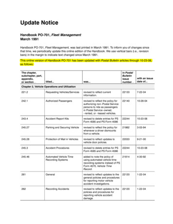
Transcription
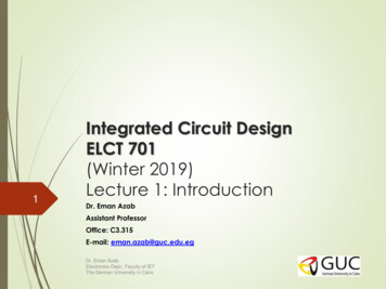
1Integrated Circuit DesignELCT 701(Winter 2019)Lecture 1: IntroductionDr. Eman AzabAssistant ProfessorOffice: C3.315E-mail: eman.azab@guc.edu.egDr. Eman AzabElectronics Dept., Faculty of IETThe German University in Cairo
2Course OverviewCourse TeamDr. Eman AzabE-mail: eman.azab@guc.edu.egOffice: C3.315Office hours: Via E-mailLecturerTeachingAssistantTeaching MethodEng.: Sandy AtefE-mail: sandy.abdelmalak@guc.edu.egOffice:C3.207Office hours: Via E-mailLocationEvaluation MethodPercentage %Assignments10One Lecture per Week(Wednesday 1st Slot)H9Quizzes15One Tutorial per Week(Tuesday 1st/3rd)Check YourScheduleMid-Term30Final45Dr. Eman AzabElectronics Dept., Faculty of IETThe German University in Cairo
Course Guidelines3 Please follow GUC regulations for attendance Course Prerequisites: SemiconductorsElectronic CircuitsElectric Circuits I and IIDigital System Design Course Objectives: Design and analyze digital circuits on transistor level Define different design alternatives in studying DynamicLogic Circuits to build high performance digital integratedcircuits Discuss different types of digital memoriesDr. Eman AzabElectronics Dept., Faculty of IETThe German University in Cairo
Tentative Course Schedule4Lecture#TopicDescription1Introduction to Integrated Circuit DesignHistorical Background on IC Industry2Revision on Semi-Conductor Devices and theirelectrical modelingPN Junctions, Transistors I-V modeling3MOS Inverter: Static BehaviorTransistor Level Implementation of Inverters(Large Signal Analysis)4CMOS Inverter: Dynamic BehaviorTransistor Level Implementation of Inverters(Transient Analysis)5Interconnect and DelayDelay introduced by wiring interconnect6Inverter: Power Consumption CalculationsStatic and Dynamic Power ConsumptionCalculations7Design of Combinational Logic Circuits (Static& Dynamic)Transistor Level Implementation of NOR, NANDand XOR Gates (Transistor Level)8Design of Sequential Logic Circuits (Static &Dynamic)Transistor Level Implementation of Latches,Flip-flops and Registers9Arithmetic Building BlocksTransistor Level Implementation of Adder,Multiplier and Shifter10 &11Design of Memory and Array StructuresTransistor Level Implementation of SRAM,DRAM, ROM transistor level12Timing Analysis for Digital IC CircuitsTiming ConstraintsDr. Eman AzabElectronics Dept., Faculty of IETThe German University in Cairo
Tentative AssessmentSchedule5Week#QuizzesAssignments4Quiz 1: Devices modeling andInverter DC CharacteristicsAssign. 1: Layout of differentInverters and their DCCharacteristics analysisAssign. 2: Static MOSCombinational Logic67Quiz 2: Dynamic CombinationallogicAssign. 3: Static & DynamicSequential Logic89Quiz 3: Sequential logic11Quiz 4: MemoriesDr. Eman AzabElectronics Dept., Faculty of IETThe German University in CairoAssign. 4: Digital IC Buildingblocks
Course Grading Rules6 Grading scheme is basedRegulations Copies will be graded as ZEROonGUC This is applicable for Assignments Stick to the office hours for questionsSend an e-mail for urgent questionsAttend the lectures and take notes!All the Course material will be available onthe websiteDr. Eman AzabElectronics Dept., Faculty of IETThe German University in Cairo
References71.“Digital Integrated Circuits: A Design Prespective”Rabaey, Chanderakasan and Nikolic2.“CMOS DigitalLeblebici3.“CMOS VLSI Design: A Circuits and SystemsPerspective”, Neil H. E. Weste and David MoneyHarrisDr. Eman AzabElectronics Dept., Faculty of IETThe German University in CairoIntegratedCircuits”,Kangand
8IC Design History andPresentOverviewDr. Eman AzabElectronics Dept., Faculty of IETThe German University in Cairo
IC History9 First Transistor was introduced in 1947 at Bell Labs, PointContact Transistor First BJT in 1949 by Schockley BJT based logic gate made by discrete components wasintroduced in 1956 by Harris Integrated Circuit concept was introduced through TexasInstruments by Jack Kilby (Nobel Prize Winner)Dr. Eman AzabElectronics Dept., Faculty of IETThe German University in Cairo
IC History10 First functioning Silicon planar IC chip (All components ona single Silicon crystal) was made by R. Noyce of FairchildCamera in 1961 It was a flip-flop circuit containing Six devicesDr. Eman AzabElectronics Dept., Faculty of IETThe German University in Cairo
IC History11 MOS transistor principle wasintroduced in 1925 by J.Lilienfeld In 1959, Dawon Kahng andMartin M. Atalla at Belllabs invented the MOS In 1963 C. T. Sah and FrankWanlass of the Fairchild R &D Laboratory showed thatlogic circuits combining pchannel and n-channelMOStransistorsinacomplementary symmetrycircuit configuration drewclose to zero power instandby mode. Wanlass patented the ideathat today is called CMOS.Dr. Eman AzabElectronics Dept., Faculty of IETThe German University in Cairo
12ASIC vs. Discrete ElectronicsDiscrete Electronics Ex.: Microphone CircuitDr. Eman AzabElectronics Dept., Faculty of IETThe German University in Cairo
13ASIC vs. Discrete ElectronicsWireless transceiver IC(Infinoen Company)Example of IC:Wireless transceiverBlock DiagramDr. Eman AzabElectronics Dept., Faculty of IETThe German University in Cairo
14ASIC vs. Discrete ElectronicsSpecificationDiscrete ed to aSpecific Part of thesystemComplete systemsexist on a small pplicationSmall ProductionMass Production(Cost decreases!)PowerHighlowDiscrete elementsTransistor sizing orexternal biasingvoltage/currentDesign parameterDr. Eman AzabElectronics Dept., Faculty of IETThe German University in Cairo
15IC History: Moore’s Law The observation made in 1965 by Gordon Moore, cofounder of Intel, that the number of transistors per squareinch on integrated circuits had doubled every year sincethe integrated circuit was invented.Dr. Eman AzabElectronics Dept., Faculty of IETThe German University in Cairo
16IC Present Day “Core i7” processor is of asize slightly greater than acoin Operates with afrequency 3.4GHzclock Minimum channel length oftransistor (2*32nm) Power: 130W with maximumsupply of 1.4V No. of transistors on Chip:1,400,000,000Dr. Eman AzabElectronics Dept., Faculty of IETThe German University in Cairo
17IC Present Day How can the design engineers integrate such a largenumber of transistors on one chip (Design level for Digitalelectronics) ? Using Divide and conquer Abstraction can be done on Digital Circuits successfully Designer focus on optimizing a standard cell and reuse it(CAD Tools are (Ex.:adder)System IC Design Course focus on the three intermediate stepsDr. Eman AzabElectronics Dept., Faculty of IETThe German University in Cairo
18IC Present Day How can the design engineers integrate such a largenumber of transistors on one chip (Design level) whendealing with analog Circuits? Abstraction can not be done in Analog world easily (Transistorsizing changes everything in the circuit) Microelectronics Course will focus on the analog design partDevice(Transistor)Dr. Eman AzabElectronics Dept., Faculty of IETThe German University in CairoCircuit(Level)System
19IC Design Flow Integrated Circuit Design Flowchart: Our course main objective is tostudy how to design basicdigital circuits used in ICs Examples: inverters, Gates, Flipflops Circuit design is done in ourcourse on Transistor level andlayout level Integrated circuit Course andVLSI courses are dedicated toDigital electronics and physicaldesign of the ICs At the end of the course, thestudent can design basic DigitalIC building blocks on the circuitlevel and on the physical level.Dr. Eman AzabElectronics Dept., Faculty of IETThe German University in Cairo
20IC Design Flow What happens when a new Technology is launched to themarket? First Step: Fabrication (FAB) companies (Ex. TSMC) provides anew technology where the MOS Channel length can bedecreased Smaller transistor means more devices can be integrated on onechip MOS can operate at lower voltage supplies (gate oxide thicknessis decreased as well) Now we reached 28nm (minimum channel length is twice this no.),they call it λ Second Step: the FAB provide the circuit level designers with amodel for the transistor nsconductance gain, parasitic capacitances, etc.)Dr. Eman AzabElectronics Dept., Faculty of IETThe German University in Cairo
21IC Design Flow What happens when a new Technology is launched to themarket? (Cont.) Third Step: Circuit level designer tries to build a basic circuitwith the new tech. and creates a model for it Designers push the new tech. to its maximum limit to get the bestperformance possible (less area, power and high speed) The basic circuit could be an inverter, gate or module dependingon the target End product Fourth Step: layout engineers start to make the physical circuitcorresponding to the basic circuit designed in previous step They draw the geometries of the drains, sources and gates of thetransistor Also they plan the contacts and connections between thetransistors in the circuit This is done using different layers of materials (Semi. Tech. Course!)Dr. Eman AzabElectronics Dept., Faculty of IETThe German University in Cairo
22IC Design Flow What happens when a new Technology is launched to themarket? (Cont.) Fifth Step: Layout Engineers must follow the FAB Design rules(DRC) The Design rules determine the minimum length the FAB cancontrol on the wafer They also define theinterconnection layersspacesbetweensamelayersand What is the separating distance between two transistors sources orgates? What is the separating distance between two layers (gate and drain ofsame transistor) Sixth Step: Layout Engineers check their layout versus thecircuit design (LVS) Final Step: Fabrication and Testing (Measurements)Dr. Eman AzabElectronics Dept., Faculty of IETThe German University in Cairo
23Digital Circuits DesignPerformance MetricsDr. Eman AzabElectronics Dept., Faculty of IETThe German University in Cairo
24Digital Circuit Design Concerns Digital wing Cost (The less the better) Area (The less the better) Functionality (Circuit is operating correctly) Robustness (What is the effect of Process Variations duringfabrication on the circuit) Performance (How fast the circuit will work?) Power and Energy Consumption (The less the better) In our course we will focus on how to calculate theseperformance metrics for Digital circuits!Dr. Eman AzabElectronics Dept., Faculty of IETThe German University in Cairo
25AppendixFabrication process of CMOS InverterDr. Eman AzabElectronics Dept., Faculty of IETThe German University in Cairo
CMOS InverterAY00111100VDDAOFFON01YONOFFAYGND0: IntroductionCMOS VLSI Design 4th Ed.26
CMOS Fabrication CMOS transistors are fabricated on silicon wafer Lithography process similar to printing press On each step, different materials are deposited oretched Easiest to understand by viewing both top andcross-section of wafer in a simplified manufacturingprocess0: IntroductionCMOS VLSI Design 4th Ed.27
Inverter Cross-section Typically use p-type substrate for nMOS transistors Requires n-well for body of pMOS transistorsAGNDVDDYSiO2n diffusionn n p p n wellp substratenMOS transistor0: Introductionp diffusionpolysiliconmetal1pMOS transistorCMOS VLSI Design 4th Ed.28
Well and Substrate Taps Substrate must be tied to GND and n-well to VDD Metal to lightly-doped semiconductor forms poorconnection called Shottky Diode Use heavily doped well and substrate contacts / tapsAGNDVDDYp n n p p n n wellp substratewelltapsubstrate tap0: IntroductionCMOS VLSI Design 4th Ed.29
Inverter Mask Set Transistors and wires are defined by masks Cross-section taken along dashed lineAYGNDVDDnMOS transistorpMOS transistorwell tapsubstrate tap0: IntroductionCMOS VLSI Design 4th Ed.30
Detailed Mask Views Six masks– n-well– Polysilicon– n diffusion– p diffusion– Contact– Metaln wellPolysiliconn Diffusionp DiffusionContactMetal0: IntroductionCMOS VLSI Design 4th Ed.31
Fabrication Chips are built in huge factories called FABs Contain clean rooms as large as football fieldsCourtesy of InternationalBusiness Machines Corporation.Unauthorized use not permitted.0: IntroductionCMOS VLSI Design 4th Ed.32
Fabrication Steps Start with blank wafer Build inverter from the bottom up First step will be to form the n-well– Cover wafer with protective layer of SiO2 (oxide)– Remove layer where n-well should be built– Implant or diffuse n dopants into exposed wafer– Strip off SiO2p substrate0: IntroductionCMOS VLSI Design 4th Ed.33
Oxidation Grow SiO2 on top of Si wafer– 900 – 1200 C with H2O or O2 in oxidation furnaceSiO2p substrate0: IntroductionCMOS VLSI Design 4th Ed.34
Photoresist Spin on photoresist– Photoresist is a light-sensitive organic polymer– Softens/hardens where exposed to lightPhotoresistSiO2p substrate0: IntroductionCMOS VLSI Design 4th Ed.35
Lithography Expose photoresist through n-well mask Strip off exposed photoresistPhotoresistSiO2p substrate0: IntroductionCMOS VLSI Design 4th Ed.36
Etch Etch oxide with hydrofluoric acid (HF)– Seeps through skin and eats bone; nasty stuff!!! Only attacks oxide where resist has been exposedPhotoresistSiO2p substrate0: IntroductionCMOS VLSI Design 4th Ed.37
Strip Photoresist Strip off remaining photoresist– Use mixture of acids called piranah etch Necessary so resist doesn’t melt in next stepSiO2p substrate0: IntroductionCMOS VLSI Design 4th Ed.38
n-well n-well is formed with diffusion or ion implantation Diffusion– Place wafer in furnace with arsenic gas– Heat until As atoms diffuse into exposed Si Ion Implanatation– Blast wafer with beam of As ions– Ions blocked by SiO2, only enter exposed SiSiO2n well0: IntroductionCMOS VLSI Design 4th Ed.39
Strip Oxide Strip off the remaining oxide using HF Back to bare wafer with n-well Subsequent steps involve similar series of stepsn wellp substrate0: IntroductionCMOS VLSI Design 4th Ed.40
Polysilicon Deposit very thin layer of gate oxide– 20 Å (6-7 atomic layers) Chemical Vapor Deposition (CVD) of silicon layer– Place wafer in furnace with Silane gas (SiH4)– Forms many small crystals called polysilicon– Heavily doped to be good conductorPolysiliconThin gate oxiden wellp substrate0: IntroductionCMOS VLSI Design 4th Ed.41
Polysilicon Patterning Use same lithography process to pattern polysiliconPolysiliconPolysiliconThin gate oxiden wellp substrate0: IntroductionCMOS VLSI Design 4th Ed.42
Self-Aligned Process Use oxide and masking to expose where n dopantsshould be diffused or implanted N-diffusion forms nMOS source, drain, and n-wellcontactn wellp substrate0: IntroductionCMOS VLSI Design 4th Ed.43
N-diffusion Pattern oxide and form n regions Self-aligned process where gate blocks diffusion Polysilicon is better than metal for self-aligned gatesbecause it doesn’t melt during later processingn Diffusionn wellp substrate0: IntroductionCMOS VLSI Design 4th Ed.44
N-diffusion cont. Historically dopants were diffused Usually ion implantation today But regions are still called diffusionn n n n wellp substrate0: IntroductionCMOS VLSI Design 4th Ed.45
N-diffusion cont. Strip off oxide to complete patterning stepn n n n wellp substrate0: IntroductionCMOS VLSI Design 4th Ed.46
P-Diffusion Similar set of steps form p diffusion regions forpMOS source and drain and substrate contactp Diffusionp n n p p n n wellp substrate0: IntroductionCMOS VLSI Design 4th Ed.47
Contacts Now we need to wire together the devices Cover chip with thick field oxide Etch oxide where contact cuts are neededContactThick field oxidep n n p p n n wellp substrate0: IntroductionCMOS VLSI Design 4th Ed.48
Metalization Sputter on aluminum over whole wafer Pattern to remove excess metal, leaving wiresMetalMetalThick field oxidep n n p p n n wellp substrate0: IntroductionCMOS VLSI Design 4th Ed.49
Layout Chips are specified with set of masks Minimum dimensions of masks determine transistorsize (and hence speed, cost, and power) Feature size f distance between source and drain– Set by minimum width of polysilicon Feature size improves 30% every 3 years or so Normalize for feature size when describing designrules Express rules in terms of l f /2– E.g. l 0.3 mm in 0.6 mm process0: IntroductionCMOS VLSI Design 4th Ed.50
Simplified Design Rules Conservative rules to get you started0: IntroductionCMOS VLSI Design 4th Ed.51
Inverter Layout Transistor dimensions specified as Width / Length– Minimum size is 4l / 2l, sometimes called 1 unit– In f 0.6 mm process, this is 1.2 mm wide, 0.6 mmlong0: IntroductionCMOS VLSI Design 4th Ed.52
Summary MOS transistors are stacks of gate, oxide, siliconAct as electrically controlled switchesBuild logic gates out of switchesDraw masks to specify layout of transistors Now you know everything necessary to startdesigning schematics and layout for a simple chip!0: IntroductionCMOS VLSI Design 4th Ed.53
About these Notes Lecture notes 2011 David Money Harris These notes may be used and modified foreducational and/or non-commercial purposes solong as the source is attributed.0: IntroductionCMOS VLSI Design 4th Ed.54
55IC Design Flowhttps://www.youtube.com/watch?v bor0qLifjz4CMOS VLSI Design 4th Ed.
Integrated Circuit Design Flow chart: Our course main objective is to study how to design basic digital circuits used in ICs Examples: inverters, Gates, Flip-flops Circuit design is done in our course on Transistor level and layout level Integrated circuit Course and VLSI