Transcription
Flexible Circuit TechnologyCHAPTER5Practical Design Guidelines for FlexINTRODUCTIONFlexible circuits are obviously unique among electronic packagingtechnologies in that they offer a wide variety of advantages unobtainableusing conventional rigid interconnection technologies. Freeformintegration of electronic elements through all three dimensions of space ishighly liberating to the design process.Such advantages, however, cannot be garnered without a thoroughunderstanding of basic flex circuit design principles. Proper use of thosedesign principles can provide a path to early success. In contrast, failureto use good design practices can result in early failure. The objective ofthis chapter is to provide information vital to the successful productionof flexible circuit designs—ones that will consistently perform to userexpectations.DESIGN PRELIMINARIESBefore embarking on a flex circuit design, it is important that a holisticoverview of the project be taken. In this overview, a circuit designershould attempt to take into account as many of the items discussed in theimplementation section as are possible or relevant. This act of taking stockof the project will help the designer appreciate the broader perspective ofthe task, minimizing the possibility that a gross and avoidable error will becarried through the design process.It is also important that the designer keep in mind that flexible circuitdesigns require a balancing of both mechanical and electrical concerns.These two competing concerns, the designer will find, often oppose eachother’s requirements in a design. It will be the holistic approach that willhelp the designer thread the needle to make the best possible choice fromgiven alternatives.USE OF MOCKUPSLet us reassert here the value of using paper doll mockups. This simplepractice will help the designer prevent many errors by exposing potential75
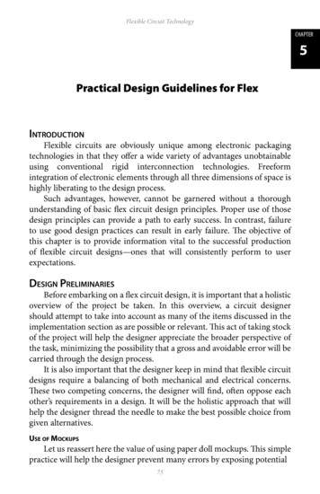
Flexible Circuit Technologyproblems early and will save both time and money.Some modern CAD systems have demonstrated the ability to executethree dimensional layouts required for flex circuit applications, but thephysical model will probably always prove of some value in addressingboth the ergonomic elements of assembly and the concerns of accessshould field repair be required.Figure 5-1 Designing with a bias for copper improves the circuit’s dimensionalstability. It may not be practical for all applications.DESIGN WITH A BIAS FOR COPPERFavoring the use of copper in design is good practice for some verysolid reasons, assuming that there are not important conflicts created bythe practice. If all other design objectives are met, then the primary reasonfor maintaining extra copper is that it helps to enhance the dimensionalstability of the circuit. Designing with a bias for copper is a practiceespecially well suited to single-layer flex circuit designs. See Figure 5-1.As indicated before, the decision to add or leave copper should bemade in light of theobjectives of the circuit’sfinal use. For example,if a reduction in weightof the final product isa key objective, thenthere would be need toFigure 5-2 Copper foil is maintained by design around circuits to provide trade away some of thebetter panel dimensional stability. Two examples are shown.enhanced dimensionalstability. Another reason for maintaining the copper is that it reduces theamount of copper etched and is thus more environmentally friendly interms of chemical usage.TOLERANCE SETTING FLEX CIRCUIT DESIGNSProper application of tolerances of flex circuit design features is a matterthat concerns both the flex circuit manufacturer and the flex circuit user.76
Flexible Circuit TechnologyIn general, it is recommended that the largest practical tolerance be givento all features and locations tofacilitate manufacture. Thisis because the base materialsare flexible and prone todistortion, making accuratemeasurement over distancesdifficult. To compensate, it isrecommended that more thanFigure 5-3 The use of multiple datums, with one being the primeone datum be used on larger and the others secondary, facilitates both accurate measurementcircuits. Individual datums of the circuit and device placement during the assembly process.can be provided locally relative to features deemed important. (See Figure5-3.) This will result in a more accurate measurement being taken and canpreempt potential conflicts in measurement results between inspectors. Toavoid confusion in design, one datum should be defined as the primary ormaster datum and others as secondary or slave datums.Tight tolerances can be attained, when required, but to do so requires*Mil-Std-2118 off ers the following statement regarding tolerances: “Drawing tolerances mustreflect bend and fold allowances between component mounting rigid areas.”Table 5-1 Tolerance guidelines for standard flex circuit manufacture. (Chart does not apply to leading edge products.)77
Flexible Circuit Technologyspecial attention and good techniques. As a result, the expense of tightertolerance circuits tends to be greater due to anticipated loss of yield. Table5-1 provides some general guidelines for tolerancing based on differentdesign standards.The values offered in Table 5-1 are rather generous by today’s standards,however. To provide a global perspective on flex circuit feature capability,a 2004 survey of 20 Japanese flexible circuit manufacturers indicated thatmore than half of the companies were routinely producing flex circuitswith traces of 110µm or less, and five companies were producing circuitswith features of 70-90µm routinely. Today are a number of flex circuitmanufacturers in Japan and elsewhere are producing circuits havingfeatures of 35 to 50µm and some have shown capabilities down to 25µmand even 10µm feature sizes.GENERAL GUIDELINES FOR DIMENSIONING AND TOLERANCINGProper dimensioning and tolerancing of flex circuits is vital toachieving good manufacturing yield. While it is not possible to point outevery possible situation where dimensions and tolerances can be used insuch a way as to confuse the interpretation of a drawing, there are certaingeneral guidelines that, if followed, can do much to minimize the potentialfor confusion. Following are a few such guidelines: Show sufficient dimensions so that the intended sizes andshapes can be determined without requiring the distancesbetween features to be calculated (or assumed). Provide individual dimensions only once and check them. State all dimensions clearly so they can onlyhave a single possible interpretation. Show the dimensions between points, lines or surfaces, whichhave a necessary and specific relation to each other or whichcontrol the location of other components or mating parts. Check dimensions to avoid accumulations of tolerancesthat may permit alternative interpretations. Provide dimensions to features, which are shown in profile makingcertain that the feature’s dimensions are not ambiguous. Do not show dimensions to lines representing hidden surfaces. Do not use “off part” datums.SPECIAL DESIGN CONSIDERATIONSThere are some unique elements of flex circuit design that require earlyconsideration. Mostly they address mechanical issues that could affectusability and/or long term performance. However, they will definitelyaffect circuit layout and so are given early consideration.78
Flexible Circuit TechnologyLAY OUT CIRCUIT TO CONSERVE MATERIALConservation of material in flexible circuit manufacture serves to helpkeep manufacturing costs down. This is important because flexible circuitmaterials tend to be expensive in comparison with standard rigid materialssuch as FR-4.We suggest accomplishing close spacing of the circuit. The techniqueof optimizing the number of circuits per panel is called nesting. The termoptimizing is used in place of the seemingly more logical term maximizingfor a reason, that reason being that the layout of a flex circuit should bebased on end use, and some uses may demand that portions of the flexcircuit be properly oriented relative to the grain direction of the foil (suchas is required for dynamic flexing). This may result in a less-than-maximummaterial use for circuit construction. However, when this is not the case,there is the opportunity to lay the circuit out in various ways to get themost out of the material.Figure 5-4 Proper circuit nesting can greatly improve panel yield and lower overall cost. Iffolding can be tolerated as an assembly operation, yield can be maximized. For dynamicflex circuit designs, the grain direction requirement may impact layout.While nesting is routinely performed by the manufacturer, the designercan aid in this process by taking advantage of the fact that flex circuits canbe bent and folded. Thus, adding a small length to a circuit arm can allow acircuit to be produced more economically, provided the user doesn’t mindadding a folding operation to his assembly process. (See Figure 5-4.)SERVICE LOOPSThe addition of a small amount of length to the flex circuit beyondthe design requirement is advisable for most flex circuit applications. Thislittle extra length of material is commonly referred to as the service looplength.79
Flexible Circuit TechnologyThe purpose of the service loop is offer sufficient length to facilitateboth assembly of the product and servicing of the product once in the field,if it should ever be required. The extra length also helps to compensate forsmall, unforeseen variations in both the package and the flex circuit.Figure 5-5 Staggered length designs facilitate bending of the flex circuit;the circuit can only be bent in one direction by design.STAGGERED LENGTH CIRCUITS (BOOKBINDER CONSTRUCTION)For ease of flexing multilayer and rigid flex designs, the use of staggeredlength design is commonly employed. The technique is accomplished byadding slightly to the length of each succeeding flex layer, moving awayfrom the bend radius. (See Figure 5-5.)A common rule of thumb isto add length equal to roughly1.5 times the individual layerthickness. This helps defeatwhatever tensor strain mighthave otherwise been built upin the outer metal layers of themultilayer flex and preventsbuckling of the center of bendlayers (see Figure 5-6).Figure 5-6 Without staggered lengths, layer buckling occurs.CONDUCTOR SIZING AND ROUTINGIn general, flex circuit conductor width and thickness are determinedby a combination of current carrying requirements, the voltage dropallowance and/or characteristic impedance control needs. When designingflex circuits for dynamic applications, the use of the thinnest possiblecopper is recommended. Thus, it is important that the designer opt forwider rather than thicker traces to accommodate basic electrical needs orrequirements. This practice assures maximum circuit flexibility.Table 5-2 can be used to determine maximum current and lineresistance for given trace widths with both 35µm (1-oz) and 70µm (2-oz)80
Flexible Circuit Technologycopper. These are relatively common foil thicknesses used in much flexcircuit manufacture, although 18µm (½-oz) and even lower copper foilthicknesses are becoming increasingly important.A number of different nomographs for determining other electricalvalues for copper have been developed to simplify copper trace-requirementspecification. The IPC’s flex circuit design specification is a good source forsuch nomographs for those who have interest. There is an effort underwayto revise these graphs, which have long been in use, to reflect more practicalvalues.ConductorWidthMaximum Currentfor 10 C rise1 oz copperConductorResistancemilliohms/ft1 oz copperMaximum Currentfor 10 C rise2 oz copperConductorRresistancemilliohms/ft2 oz 5Table 5-2 Current Carrying Capacity of Conductors. Conductor width and copper thicknesshave a direct impact on the current carrying capacity of a flexible circuit. The abovetable provides a means of determining the conductor width for a 10 C riseTrace Width MinimumsThe minimum practical trace width for a flex circuit varies from vendorto vendor. Flex circuits with traces 250µm (0.010") and greater are fairly easyto obtain; however, line widths 125µm (0.005") and lower are increasinglycommon. Flex circuits having features in the range of 50µm (0.002") andlower are available in volume production from a limited number of vendors,but the number of such vendors is growing to keep pace with the demandfor ever smaller electronic products.The type of technology used in circuit feature manufacture also heavilyinfluences trace width minimums. For example, plated up copper sputteredpolyimide base circuits are basically limited in feature size only by the81
Flexible Circuit Technologyphotolithographic capabilities of the manufacturer. Thus, very small circuitfeatures can be made. For etched circuit traces, however, the trace widthand pitch are influenced primarily by the thickness of the base copper foil.Typically, the trace pitch limit is nearly linear with copper thicknesswithin a narrow range. 18µm (½-oz) copper will yield circuit features ata 125µm (0.005") pitch, while with 35µm (1-oz) copper, etching becomesmore difficult under 175µm (0.007") pitch. While some manufacturers cansuccessfully produce 25µm (0.001") features with 18µm copper, vendorcapabilities vary widely. It is best to check with the fabricator beforeattempting to design very fine line features.CONTROLLED IMPEDANCE LINESControlled impedance transmission cabling is a popular applicationfor flex circuits, and the value of such product is increasing as digital datasignaling speeds continue to rise.Tighter tolerances for etched features are possible with flex circuitsbecause of the lower profile adhesion treatment or “tooth” of the copper.The use of thicker flexible dielectric substrates, if the design allows, canease somewhat the etching challenge because thicker substrates allow forwider signal lines, which can be fabricated more easily to meet the tighttolerances needed for controlled impedance circuits. This topic will bediscussed in more detail later in this chapter.ETCH FACTORSAn etch factor is a tool used by the manufacturer to compensate forisotropic etching process effects. It is recommended that the designercheck with the vendor to determine if they want inclusion of an etch factor.Usually it is best if the manufacturer makes this adjustment, as they will bemost familiar with their process and its capability.Figure 5-7 The etching process works laterally as well as down, at a ratio of roughly 1:2 laterally to downThe typical line width loss (measured at the top of the trace) due to theetching process is approximately 2x copper foil thickness, although coppertype, conductor pitch, etch mask, process chemistry and equipment can allinfluence the results.82
Flexible Circuit TechnologyCONDUCTOR ROUTING CONCERNSThere are a few general issues related to conductor routing of a flexcircuit. The first item of concern is keeping to a minimum the number ofcrossovers in the layout. This will help to keep the layer count down andlower the cost. Newer CAD systems can respond to such a requirement,but the results may need to be massaged or optimized to make certain thatthe smallest possible area has been consumed in the process.Routing of conductors on a flexible circuit perpendicular to bend andfold is the recommended design practice. The purpose is to facilitate thebending or folding process and to minimize stress through the area. Inaddition, circuitry should be routed on a single copper layer through bendand fold areas whenever possible.Figure 5-8 Routing options for flex circuit trace corners. Avoid sharp corners if possible. A radius isbest as it provides a smooth transition and mitigates potential issues related to stress risers.It is also recommended that designs avoid having right or acute angles( 90 ) in circuit routing. This is because they tend to trap solution and mayover etch in process. They are also more difficult to clean after processing,so best practice dictates that corners should be provided with a radius ifpossible. The radius also improves signal propagation, as the reflections atturns are reduced.With double-sided flex, when and where the conductors must berouted through bend and fold areas and when copper traces are on bothsides, the circuit designer should design spaces to be approximately 2-2.5xthe trace width.Preferably, the designer should also stagger traces from side to side.The purpose of this practice is to avoid the I-beam effect. This can be acritical concern in dynamic applications. (See Figure 5-9.)83
Flexible Circuit TechnologyFigure 5-9 I-Beamed vs. Staggered Conductors. I-beamed constructions increase the stiffness of the circuit throughbend and fold areas. A better alternative, if space allows, is to stagger conductors for improved flexibility.Finally, placement of vias within the bend area is highly discouragedas they will adversely affect bend formation and create unwanted points ofstress and potential crack propagation.GROUND PLANE DESIGNGround areas should be crosshatched if electrical consideration of thedesign will allow for such. The practice helps both to reduce weight andimprove circuit flexibility. The size of the openings in the ground planemay be critical depending on the end product requirements for shieldingor controlling of characteristic impedance. If openings are too large,some shielding effects may be lost, depending on frequency. Also, groundconnections for components should be thermally relieved to reduce heatsinking and assure formation of a good solder joint. This is accomplishedby etching a clearance area around the pad while maintaining electricalconnection. Figure 5-10 illustrates the technique.Figure 5-10 Ground planes should be crosshatched if possible to improve flexibility. Clearance holesprevent shorting. Ground connections should be relieved to reduce heat sinking when soldering.84
Flexible Circuit TechnologyPOLYMER THICK FILM DESIGN GUIDELINESDue to their unique nature, polymer thick film (PTF) circuits have theirown very specific design rules. As a screen printing based technology, thelimits of design are tied to two main factors: (1) the conductivity of the inkchosen and the limits of the screen-printing materials, and (2) the processesused. Much of the latter factor is tied to the former. That is, the particlesize of the included conductor material and the polymer carrier will helpestablish the limits of screen printing. Emerging nanoparticle technologiescould boost conductivity significantly, possibly opening the door forbroader use of polymer thick film technology. While PTF circuits are notgenerally considered for dynamic applications, they can actually performquite well in certain dynamic applications. Some experimenters havereported increases in conductivity with cycling. PTF membrane switchesalso stand as witnesses to the efficacy of PTF as a flexing technology.CONDUCTOR WIDTH AND SPACING FOR PTFGenerally, minimum conductor width and spacing is considered to bein the range of 375µm (0.015"). It is possible to produce finer lines andspaces using PTF inks, but conductivity can become more of a designperformance concern.CURRENT CARRYING CAPACITY OF PTFSilver-based polymer thick film inks, under normal conditions, canbe expected to carry approximately 25% of the current of copper circuitsfor equivalent line widths and nominal PTF ink thickness. Care shouldbe used, however, in attempting to maximize conductor current-carryingcapability under this premise. Hot spots within the conductor matrix cancause rapid degradation of the conductor and possible failure.SCREEN-PRINTED PTF RESISTORSScreen-printed resistors are fairly commonly incorporated into PTFcircuit designs. If used in a design, the resistors should be kept to a minimu
TOLERANCE SETTING FLEX CIRCUIT DESIGNS Proper application of tolerances of ex circuit design features is a matter that concerns both the ex circuit manufacturer and the ex circuit user. Figure 5-1 Designing with a bias for