Transcription
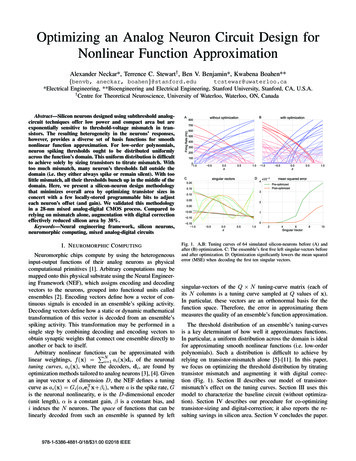
Optimizing an Analog Neuron Circuit Design forNonlinear Function ApproximationAlexander Neckar*, Terrence C. Stewart† , Ben V. Benjamin*, Kwabena Boahen**{benvb, aneckar, al Engineering, **Bioengineering and Electrical Engineering, Stanford University, Stanford, CA, U.S.A.†Centre for Theoretical Neuroscience, University of Waterloo, Waterloo, ON, CanadaAbstract—Silicon neurons designed using subthreshold analogcircuit techniques offer low power and compact area but areexponentially sensitive to threshold-voltage mismatch in transistors. The resulting heterogeneity in the neurons’ responses,however, provides a diverse set of basis functions for smoothnonlinear function approximation. For low-order polynomials,neuron spiking thresholds ought to be distributed uniformlyacross the function’s domain. This uniform distribution is difficultto achieve solely by sizing transistors to titrate mismatch. Withtoo much mismatch, many neuron’s thresholds fall outside thedomain (i.e. they either always spike or remain silent). With toolittle mismatch, all their thresholds bunch up in the middle of thedomain. Here, we present a silicon-neuron design methodologythat minimizes overall area by optimizing transistor sizes inconcert with a few locally-stored programmable bits to adjusteach neuron’s offset (and gain). We validated this methodologyin a 28-nm mixed analog-digital CMOS process. Compared torelying on mismatch alone, augmentation with digital correctioneffectively reduced silicon area by 38%.Keywords—Neural engineering framework, silicon neurons,neuromorphic computing, mixed analog-digital circuitsI. N EUROMORPHIC C OMPUTINGNeuromorphic chips compute by using the heterogeneousinput-output functions of their analog neurons as physicalcomputational primitives [1]. Arbitrary computations may bemapped onto this physical substrate using the Neural Engineering Framework (NEF), which assigns encoding and decodingvectors to the neurons, grouped into functional units calledensembles [2]. Encoding vectors define how a vector of continuous signals is encoded in an ensemble’s spiking activity.Decoding vectors define how a static or dynamic mathematicaltransformation of this vector is decoded from an ensemble’sspiking activity. This transformation may be performed in asingle step by combining decoding and encoding vectors toobtain synaptic weights that connect one ensemble directly toanother or back to itself.Arbitrary nonlinear functions N can be approximated withlinear weightings, f (x) i 1 ai (x)di , of the neuronaltuning curves, ai (x), where the decoders, di , are found byoptimization methods tailored to analog neurons [3], [4]. Givenan input vector x of dimension D, the NEF defines a tuningcurve as ai (x) Gi (αi eTi x βi ), where a is the spike rate, Gis the neuronal nonlinearity, e is the D-dimensional encoder(unit length), α is a constant gain, β is a constant bias, andi indexes the N neurons. The space of functions that can belinearly decoded from such an ensemble is spanned by left978-1-5386-4881-0/18/ 31.00 2018 IEEEFig. 1. A,B: Tuning curves of 64 simulated silicon-neurons before (A) andafter (B) optimization. C: The ensemble’s first five left singular-vectors beforeand after optimization. D: Optimization significantly lowers the mean squarederror (MSE) when decoding the first ten singular vectors.singular-vectors of the Q N tuning-curve matrix (each ofits N columns is a tuning curve sampled at Q values of x).In particular, these vectors are an orthonormal basis for thefunction space. Therefore, the error in approximating themmeasures the quality of an ensemble’s function approximation.The threshold distribution of an ensemble’s tuning-curvesis a key determinant of how well it approximates functions.In particular, a uniform distribution across the domain is idealfor approximating smooth nonlinear functions (i.e. low-orderpolynomials). Such a distribution is difficult to achieve byrelying on transistor-mismatch alone [5]-[11]. In this paper,we focus on optimizing the threshold distribution by titratingtransistor mismatch and augmenting it with digital correction (Fig. 1). Section II describes our model of transistormismatch’s effect on the tuning curves. Section III uses thismodel to characterize the baseline circuit (without optimization). Section IV describes our procedure for co-optimizingtransistor-sizing and digital-correction; it also reports the resulting savings in silicon area. Section V concludes the paper.
conductances [13], [14]. Each conductance is modeled by asingle transistor, whose mismatch is captured by its currentgain parameter. We express the fraction ζi,j of the currentinjected into node i that flows to ground at node j in terms ofthese current-gains. Thus, the two networks’ outputs at node jsydcIsy,i (t) and ζi,jIDC , for Isy,i (t) and IDC , respectively.are ζi,jC. SomaThe j th soma’s input current J(t) is obtained fromdcand ζi,jIDC , the diffusor-networks’ outputs, asfollows. A programmable offset current—denoted by γjsy Iband γjdc Ib , respectively—is first added if desired; Ib ’s valueis set globally. If added, γjsy and γjdc may have one of threenvalues, described by γjsy k 1 ΛPk for n 1, 2, 3, whereΛP1 3 capture the switched current-sources’ transistor mismatch; ΛN1 3 play a similar role for γjdc . After the differencebetween the resulting currents is rectified, a programmablegain, ξj , is applied. n It may have one of four values, describedby ξj ΛG1 /( k 1 ΛGk ) for n 1, 2, 3, 4, where ΛG1 4capture transistor-mismatch. Thus, we have sydcζi,j Isy,i (t) ζi,j IDC γj Ib , I0(2)J(t) ξj maxsyIsy,i (t)ζi,jFig. 2. The neuron is comprised of—from left to right—a pulse-extender, alowpass temporal filter (synapse), a pair of lowpass spatial filters shared withthe other neurons (diffusor network), a rectifier with programmable bias andgain, and a relaxation oscillator (soma).II. S ILICON -N EURON R ESPONSE C URVEThe neuron receives excitatory or inhibitory spikes, converts them into current pulses (pulse-extender), filters thesepulses temporally (synapse) as well as spatially (diffusornetwork), and converts the resulting current into a spike train(soma) (Fig. 2). All these operations are subject to transistormismatch, which may be modeled by current-gain parameters(denoted by Λi for transistor i) that are log-normally distributed with median equal to one.A. Pulse-Extender and SynapseOur pulse-extender accepts an excitatory or inhibitory spikeand, after a nominal delay Toff , generates a current pulse,IP (t), with nominal duration Ton and nominal amplitudeIEXC IDC ΔI or IINH IDC ΔI. Thus, if thespike arrives at time 0, IP (t) IDC ΔI from Λoff Toffto Λoff Toff Λon Ton , where Λoff and Λon capture the overall mismatch between different pulse-extenders. Outside thisinterval, IP (t) is nominally equal to IDC . When excitatory( ) or inhibitory ( ) spikes arrive with interspike intervalTon(IDC ΔI). It saturates atTspk , IP (t)’s mean value is ΛTonspkΛon TonΛon Ton Λoff Toff (IDC ΔI) when Tspk Λon Ton Λoff Toff .Our synapse’s circuit-design is similar to [3], [12]. Accounting for transistor-mismatch, its output, Isy (t), obeysdIsyΛ 2 Λ4 (Λ6 Λ5 )Isy (t) Λ5 IP (t)τsydtΛ1 Λ3(1)where τsy is its time-constant. Λ1 4 correspond to ML1 4 in[3]’s Fig. 3, while Λ5 and Λ6 , which have median 1 and 2,respectively, correspond to Iτ2 and Iτ1 Iτ2 in [3]’s Fig. 3.Λ52 Λ4In steady-state, Isy (t) ΛΛ1 Λ3 Λ6 Λ5 IP (t). This current isinjected into the diffusor network. Each of the pulse-extender’sand synapse’s programmable parameters (IEXC , IINH , IDC ,Ton , Toff , and τsy ) share a common global bias.B. Diffusor networkWe use two diffusor networks, one for the synaptic output(Isy,i (t)) and the other for a reference current (IDC ). Thediffusor network emulates current spread in a hexagonalresistive network and supports globally programmable horizontal (between neighboring nodes) and vertical (to ground)978-1-5386-4881-0/18/ 31.00 2018 IEEEiγjsy γjdcwhere γj and I0 is the (transistor) leakage current.Our soma’s relaxation oscillator is a modified axon-hillockcircuit [15]. Our modification adds a logarithmic dependenceto the interspike interval’s inversely proportional dependenceon the steady-state input current J: 2 Λ d k21 Λk1k0Λa Λc J ln(3)Tspk 2 Λ d k3Λa JΛa J1 ΛΛa Λc JThe pulse-width, which serves as a refractory period, has asimilar dependence on a bias current, Iref , fed to the inputduring this phase: b Λ4 m21 Λm0m1Λ1 Λ3 Iref ln(4)Tref b Λ4 m3Λ1 IrefΛ1 Iref1 ΛΛ1 Λ3 IrefΛa d and Λ1 4 capture transistor-mismatch; k0 3 and m0 3are constant circuit-design parameters.III. BASELINE N EURON B EHAVIORIn order to present a continuous signal, x(t), to an ensembleof silicon neurons, we convert it into a train of excitatoryand inhibitory spikes. For x(t) 1, ηfmax eps (excitatoryspikes per second) will be fed into one group of synapsesand ηfmax ips (inhibitory-spikes per second) will be fed intoanother group of synapses. For x(t) 1, the first group willreceive ηfmax ips and the other group will receive ηfmax eps.These rates are linearly interpolated to x(t) 0, where nosynapses receive any spikes. The fraction η 0.6 of fmax 1/(Ton Toff ) that we use is chosen to avoid saturation—evenfor outliers—as well as to allow x(t) 1 to be encodedby a mix of excitatory and inhibitory spikes (the case duringdecoding). For multiple continuous signals, x(t), this same
Fig. 3. Spike-rates of 64 simulated silicon-neurons for different inputs x withno mismatch (A) and with mismatch and baseline transistor sizes (B).Fig. 4. Distribution of effective gains and biases across 16 ensembles with64 simulated silicon-neurons each (1,024 samples in total). A: With baselinesized, mismatched, transistors. B: After optimizing transistor-sizing and biasbit and gain-bit settings. Neurons above the upper line always spike, neuronsbelow the lower line (red) never spike, and neurons between the lines crossthreshold somewhere in the [ 1, 1] range (good fraction).B. Behavior With MismatchIf we include transistor mismatch in our simulation, weobtain heterogeneous tuning-curves that are useful for approximating functions (Fig. 3B). The most useful neurons are thosethat start spiking somewhere inside the input range. Thosethat spike throughout the input range are not as useful. Andthose that do not spike at any input value are useless. Whileidentifying these three groups of neurons is straightforwardwhen the ensemble is presented with a single continuoussignal, this task becomes unwieldy when it is presented withmultiple continous signals (i.e. x(t) is multidimensional).To easily identify the three groups of neurons, even for amultidimensional ensemble, we introduce the cone plot. Thisplot visualizes an ensemble’s distribution of gains (αj ) andbiases (βj ). To generate it, we compute the transformationneeded to convert each tuning curve into an ideal tuningcurve. If the ideal neuron’s response to its input current J isGideal (J), we find the j th neuron’s effective gain αj and biasβj such that its tuning curve Gj (x) Gideal (αj eTj x βj ).For x(t) one-dimensional, e 1 (e.g., the neurons on theright ( 1) and on the left ( 1) in Fig. 3A). Referring back toJ’s expression, we find that syαj ξj (1 1 )ζi,jηΛsy,i ΛPG,i ΔI (6) i sydc(7)(1 1 )(Λsy,i ζi,j ζi,j )IDC γj Ibβ j ξjiprocess applies to each dimension, with each signal’s spiketrain targeting its own (non-overlapping) set of synapses.These spikes are extended and filtered, producing currentthat the diffusor network spreads and feeds into each soma,similar to [5]. The j th one’s net positive input is syΔΔJi x (1 1 )ζi,jIDC γj Ib (5)J ξj (1 1 )ζi,jiwhere 1 [i] and 1 [i] are indicator functions for the twogroups of synapses, ΔJ ηΛsy ΛPG ΔI, and ζ Δ Λsy ζ sy TonΛ52 Λ4and Λsy Λζ dc . Here, ΛPG Λon TΛonon ΛΛ1 Λ3 Λ6 Λ5 areoff Toffthe gains of the pulse-extender and synapse, respectively.A. Behavior Without MismatchTo demonstrate that some mismatch is necessary forfunction-approximation, we use the silicon-neuron model (seeSection II) to simulate 64 neurons receiving a single continuous signal, x(t), with no transistor-mismatch (Fig. 3A). Differences among their responses arise solely from the differentdistances that synaptic input has to spread through the diffusornetwork to reach them. For x(t) 0, they will not spike. Forx(t) 0, those closer to synapses receiving excitatory spikeswill spike; the more positive x(t) is, the more quickly theyspike. For x(t) 0, the second set of synapses will now bereceiving excitatory spikes, and neurons closer to them willnow spike. Without mismatch, all the neurons’ tuning curvesare scaled versions of each other. Consequently, the ensembleis nearly worthless for function-approximation.978-1-5386-4881-0/18/ 31.00 2018 IEEENotice that, for e 1 or 1, the neuron spikes if x βj /αj or x βj /αj , respectively. Therefore, its thresholddoes not depend on ξj , the programmable gain.The three groups of neurons fall neatly into the cone plot’sthree regions (Fig. 4A). For our baseline transistor-sizing (seebelow), only 48.2% of the ensemble is in the good group(i.e. 1 βj /αj 1). βj /αj ’s spread—see the expressionsabove—arises mainly from the synapses’ mismatched gains(Λsy,i ), which are determined by four transistors.1 Therefore,we explored the trade-off between sizing-up these transistorsversus adding switched-current sources to increase the numberof programmable offset-current levels (γj ) that we can choosefrom to push neurons above the cone down (γj 0) and pushthose below the cone up (γj 0).IV. O PTIMIZATIONTo find the optimal trade-off between allocating area tothe synapse’s transistors or allocating it to switched-currentsources, we swept these quantities simultaneously, measuringthe good fraction of the ensemble for a variety of configurations. On one hand, quadrupling a transistor’s channel-areaonly halves the standard deviation of the Gaussian underlyingits current-gain’s log-normal distribution [16]. On the otherhand, with n 1 equally-sized switched current-sources,log2 (n) bits programmed into SRAM can be translated inton 1 levels of current (or gains).1 That is, Λ , Λ , Λ , & Λ . Λ arises from a transistor in a global-bias23561circuit and Λ4 is identical to preserve symmetry.
Fig. 5. Good fraction versus width of four key transistors (normalized tobaseline). This fraction increases dramatically as the number of offset-currentlevels the optimization algorithm chooses from increases. Whiskers indicatethe 2.5th and 97.5th percentile of the distribution of fractions of good neuronsacross 2,000 samples of 64-neuron ensembles.A. Transistor Sizing and Programmable Bias-LevelsWe program γj , the j th neuron’s bias, as follows. Givenn 1 levels to choose from, we select the one that yields 1 βj /αj 1 (i.e. inside the cone). If more than onesatisfy this requirement, we choose randomly among them.If none satisfy it, each level either satisfies βj /αj 1(never spikes for e 1) or βj /αj 1 (always spikesfor e 1). Of the former, all choices are useless. Of thelatter, we choose the lowest level, which gives us access tothe steepest and most nonlinear part of the tuning-curve. Sincethe neuron’s programmable gain, ξj , does not affect the βj /αjratio, we program it independently to obtain maximum spikerates between 100 and 1,000 spike/s, choosing randomly ifmore than one gain-level satisfies this requirement.By simultaneously optimizing the synapse’s transistor-sizingand the number of programmable offset-current levels (n 1),we found that more than seven levels (including zero) givesdiminishing returns (Fig. 5). Furthermore, seven levels improve yield to such a degree that more than doubling thebaseline-width (W 160 nm) does not provide significantimprovement; lengths are kept at baseline (L 450 nm).Doubling the width left room to spare in the layout, as its areawas dominated by capacitors, which were implemented in themetal layers. Thus, we were at liberty to quadruple the widthof the two transistors that contribute to τsy ’s mismatch (i.e. toΛ5 & Λ6 ). With all these optimizations, the yield increasedfrom Y 0.482 to Ỹ 0.896 (Fig. 4B). If we consider thedistribution’s 2.5th percentile, instead of its mean, the yieldincreases from 0.062 to 0.812—even more dramatic.B. Silicon Area SavingsWe compute the effective area our optimized design needsto yield a fixed number of good neurons and compare it to thatan unoptimized version of the design needs. In our fabricatedlayout, four somas share a synapse and sixteen neurons share a978-1-5386-4881-0/18/ 31.00 2018 IEEEFig. 6. Transistor Layout. M: Portion of SRAM showing 64 bits shared byeight somas and two synapses. The row decoder (D) and an 8T bit-cell (C)are outlined. So: Soma with programmable gain (G), bias (B & B-), andassociated logic (Bctrl) outlined. Sy: Synapse with area increases related toΛ5 & Λ6 (T5, T6) and Λ2 & Λ3 (T2, T3) outlined. AER circuitry is notshown. Note the relative sizes of analog (thick-oxide) and digital (thin-oxide)transistors in this 28-nm process.SRAM and an AER transceiver (Fig. 6). Hence, the optimizeddesign’s area per neuron (μm2 ) isÃneu Asoma Asyn /4 (ASRAM AAER )/16 27.7 42.2/4 (78.8 566.5)/16 78.6(8)To compute the unoptimized design’s area per neuron, wesubtract the area sizing-up the synapse’s transistors takes aswell as the area programmable gain- and offset-circuitry takes.Four switched current-sources controlled by two bits implement four gains and six switched current-sources controlledby three bits implement six nonzero offsets. Hence, we haveAneu Ãneu ΔAsyn /4 Again Abias (2 3)Abit 78.6 1.15 6.22 5 0.616 68.2(9)Thus, optimization added 10.4 μm2 .The two versions’ effective areas are Aneu /Y 141.5 μm2and Ãneu /Ỹ 87.7 μm2 , since we have to fabricate 1/Yneurons to get one good neuron. Thus, the effective-areasaving is S (Aneu /Y Ãneu /Ỹ )/(Aneu /Y ) 0.38.V. C ONCLUSIONWe showed how the quality of a silicon-neuron ensemble’s function-approximation can be enhanced by cooptimizing transistor-sizing (to titrate mismatch) and programmable offset-current levels (to rescue outliers). Our solution reduced silicon area by 38% while tightening the yielddistribution considerably. Our approach is readily applicableto ensembles that receive multiple continuous signals, thussupporting multidimensional function approximation.ACKNOWLEDGMENTThis work was supported by ONR grants N000141310419and N000141512827.
R EFERENCES[1] K. Boahen, “A Neuromorph’s Prospectus”, Computing in Science &Engineering, vol. 19, no. 2, pp. 14-28, 2017.[2] C. Eliasmith and C. Anderson, Neural Engineering: Computation, representation, and dynamics in neurobiological systems, MIT Press, Cambridge MA, 2003.[3] A. R. Voelker, B. V. Benjamin, T. C. Stewart, K. Boahen and C. Eliasmith, “Extending the neural engineering framework for nonideal silicon synapses”, IEEE International Symposium on Circuits and Systems (ISCAS), pp. 1-4, Baltimore MD, May 2017. doi: 10.1109/ISCAS.2017.8050810[4] E. Kauderer-Abrams, A. Gilbert, A. Voelker, B. Benjamin, and T. C. Stewart, and K. Boahen, “A Population-Level Approach to TemperatureRobustness in Neuromorphic Systems”, IEEE International Symposiumon Circuits and Systems (ISCAS), pp. 1-4, Baltimore MD, May 2017. doi:10.1109/ISCAS.2017.8050985[5] S. Choudhary, S. Sloan, S. Fok, A. Neckar, E. Trautmann, P. Gao,T. Stewart, C. Eliasmith, and K. Boahen, “Silicon Neurons that Compute”, ICANN 2012: 22nd International Conference on Artificial NeuralNetworks, pp. 121-128, Lausanne, Switzerland, September 2012. doi:10.1007/978-3-642-33269-2 16[6] A. Basu, S. Shuo, H. Zhou, M. H. Lim, and G.-B. Huang, “Silicon spikingneurons for hardware implementation of extreme learning machines”,Neurocomputing, vol. 102, pp. 125-134, February 2013.[7] S. Menon, S. Fok, A. Neckar, O. Khatib and K. Boahen, “Controlling articulated robots in task-space with spiking silicon neurons”, 5thIEEE RAS/EMBS International Conference on Biomedical Robotics andBiomechatronics, pp. 181-186, Sao Paulo BRAZIL, August 2014, doi:10.1109/BIOROB.2014.6913773[8] F. Corradi, C. Eliasmith, and G. Indiveri, “Mapping arbitrary mathematical functions and dynamical systems to neuromorphic VLSI circuitsfor spike-based neural computation, Proc. IEEE Int. Symp. CircuitsSyst. (ISCAS), pp. 269-272, June 2014.978-1-5386-4881-0/18/ 31.00 2018 IEEE[9] O. Richter, R. F. Reinhart, S. Nease, J. Steil, and E. Chicca, “Devicemismatch in a neuromorphic system implements random features forregression, Proc. IEEE Biomed. Circuits Syst. Conf. (BioCAS), pp. 1-4,October 2015.[10] C. S. Thakur, R. Wang, T. J. Hamilton, J. Tapson, and A. van Schaik,“A low power trainable neuromorphic integrated circuit that is tolerant todevice mismatch”, IEEE Transactions on Circuits and Systems I: RegularPapers, vol. 63, no. 2, pp. 211-221, 2016.[11] C. S. Thakur, R. Wang, T. J. Hamilton, R. Etienne-Cummings, J. Tapsonand A. van Schaik, “An Analogue Neuromorphic Co-Processor ThatUtilizes Device Mismatch for Learning Applications”, IEEE Transactionson Circuits and Systems I: Regular Papers, vol. xx, no. yy, pp. 1-11, 2017.doi: 10.1109/TCSI.2017.2756878[12] W. Himmelbauer and A. G. Andreou, “Log-domain circuits in subthreshold MOS, Proceedings of the 40th IEEE Midwest Symposium on Circuitsand Systems, vol. 1. pp. 26-30, 1997.[13] K. A. Boahen and A. G. Andreou, “A Contrast Sensitive Silicon Retinawith Reciprocal Synapses”, Advances in Neural Information ProcessingSystems, J. E. Moody and R. P. Lippmann, Eds., vol. 4, pp. 764-772,Morgan Kaufmann, San Mateo CA, 1992.[14] A. G. Andreou and K. A. Boahen, “Translinear circuits in subthresholdMOS”, Analog Integr. Circuits Signal Process., vol. 9, no. 2, pp. 141-166,1996.[15] C. Mead, Analog VLSI and Neural Systems, Addison-Wesley, BostonMA, 1989.[16] A. Pavasović, A. G. Andreou, and C. R. Westgate, “Characterization ofsubthreshold MOS mismatch in transistors for VLSI systems”, Journal ofVLSI signal processing systems for signal, image and video technology,vol. 8, no. 1, pp. 75-85, 1994. doi: 10.1007/BF02407112
Optimizing an Analog Neuron Circuit Design for Nonlinear Function Approximation Alexander Neckar*, Terrence C. Stewart†, Ben V. Benjamin*, Kwabena Boahen** {benvb, aneckar, boahen}@stanford.edu tcstewar@uwaterloo.ca*Electrical Engineering, **Bioengineering and Electric